 | –≠–ª–µ–∫—Ç—Ä–æ–Ω–Ω—ã–π –∫–æ–º–ø–æ–Ω–µ–Ω—Ç: LH7A404-1 | –°–∫–∞—á–∞—Ç—å:  PDF PDF  ZIP ZIP |

Advance Data Sheet
1
LH7A404
Advance Data Sheet
32-Bit System-on-Chip
FEATURES
∑ ARM922TTM Core:
≠ 32-bit ARM9TDMITM RISC Core (200 MHz)
≠ 16KB Cache: 8KB Instruction Cache and 8KB
Data Cache
≠ MMU (Windows CETM Enabled)
∑ 80KB On-Chip Memory
∑ Vectored Interrupt Controller
∑ External Bus Interface
≠ 100 MHz
≠ Asynchronous SRAM/ROM/Flash
≠ Synchronous DRAM/Flash
≠ PCMCIA
≠ Compact Flash
∑ Clock and Power Management
≠ 32.768 kHz and 14.7456 MHz Oscillators
≠ Programmable PLL
∑ Low Power Modes
≠ Run (200 mA), Halt, Standby (35
µ
A)
∑ Programmable LCD Controller
≠ Up to 1,024 ◊ 768 Resolution
≠ Supports STN, Color STN, HR-TFT, TFT
≠ Up to 64 k-Colors and 15 Gray Shades
∑ 10 Channel, 10-bit A/D Converter
≠ Touch Screen Controller
≠ Brownout Detector
∑ DMA (12 Channels)
≠ External DMA Channels
≠ AAC (AC97)
≠ MMC
≠ USB
∑ USB Host and Device Interface (USB1.1)
∑ Synchronous Serial Port (SSP)
≠ Motorola SPITM
≠ Texas Instruments SSI
≠ National MICROWIRETM
∑ PS/2 Keyboard/Mouse Interface (KMI)
∑ Three Programmable Timers
∑ Three UARTs
≠ Classic IrDA (115 kbit/s)
∑ Smart Card Interface (ISO7816)
∑ Four Pulse Width Modulators (PWMs)
∑ MultiMediaCard Interface with Secure Digital
(MMC 2.11/SD 1.0)
∑ AAC (AC97) Codec Interface
∑ Smart Battery Monitor Interface
∑ Real Time Clock (RTC)
∑ Up to 64 General Purpose I/O Channels
∑ Programmable Interrupt Controller
∑ Watchdog Timer
∑ JTAG Debug Interface and Boundary Scan
∑ Operating Voltage
≠ 1.8 V Core
≠ 3.3 V Input/Output (1.8 V I/O Optional*)
∑ Temperature
≠ 0∞C to +70∞C Commercial
≠ -40∞C to +85∞C Industrial (With Clock Frequency
Reduction*)
∑ 324-Ball PBGA Package
DESCRIPTION
The advent of 3G technology opens the door for a
wide range of Multimedia applications in mobile infor-
mation appliances. These appliances require high pro-
cessing performance and low power consumption. The
LH7A404 is designed from the ground up to provide
high processing performance, low power consumption,
and a high level of integration.
The LH7A404 contains a high performance 32-bit
ARM922T Core. Power consumption is reduced by the
high level of integration, 80KB on-chip SRAM, fully static
design, power management unit, low voltage operation
(1.8 V Core, 1.8 V or 3.3 V I/O) and on-chip PLL.
Motorola SPI is a trademark of Motorola, Inc.
National Semiconductor MICROWIRE is a trademark of
National Semiconductor Corporation.
ARM922T and ARM 9TDMI are trademarks of Advanced RISC Machines
(ARM) Ltd.
Windows CE is a trademark of Microsoft Corporation.
NOTE: *Under development. Results pending further
characterization.

LH7A404
32-Bit System-on-Chip
2
Advance Data Sheet
Figure 1. LH7A404 Block Diagram
LH7A404-1
OSCILLATOR,
PLL1 and PLL2, POWER
MANAGEMENT, and
RESET CONTROL
VECTORED
INTERRUPT
CONTROLLER
REAL TIME
CLOCK
14.7456 MHz
32.768 kHz
SYNCHRONOUS
MEMORY
CONTROLLER
PCMCIA/CF
CONTROLLER
COLOR LCD
CONTROLLER
80KB
SRAM
LCD AHB
BUS
ASYNCHRONOUS
MEMORY
CONTROLLER
EXTERNAL
BUS
INTERFACE
ARM 922T
ADVANCED
PERIPHERAL
BUS BRIDGE
DMA
CONTROLLER
ADVANCED
HIGH-PERFORMANCE
BUS (AHB)
ADVANCED
PERPHERAL
BUS (APB)
HR-TFT
LCD TIMING
CONTROLLER
USB HOST
INTERFACE
GENERAL
PURPOSE I/O
(64)
SYNCHRONOUS
SERIAL PORT
TIMER (3)
BATTERY
MONITOR
INTERFACE
USB DEVICE
INTERFACE
WATCHDOG
TIMER
IrDA
INTERFACE
UART (3)
MULTIMEDIA CARD/
SECURE DIGITAL
INTERFACE
SMART CARD
INTERFACE
(ISO7816)
PWM (4)
PS/2 INTERFACE
A/D
TOUCH SCREEN
CONTROLLER
CODEC
INTERFACE
AC97
COLOR LCD
CONTROLLER

32-Bit System-on-Chip
LH7A404
Advance Data Sheet
3
Table 1. Functional Pin List
BGA
SIGNAL
DESCRIPTION
OUTPUT
DRIVE
J9
VDD
I/O Ring Power
K9
M9
N9
P9
P11
P12
P13
P14
N14
M14
L14
K14
J14
J13
J11
J10
E4
VSS
I/O Ring Ground
H4
L4
R4
W8
W11
W15
W19
T19
P19
M19
K19
G19
D18
D14
D10
D7
K3
VDDC
Core Power
Y5
Y12
V20
N20
H20
D20
C12
C8
F3
LH7A404
32-Bit System-on-Chip
4
Advance Data Sheet
G2
VSSC
Core Ground
M2
AA6
AA15
P21
K21
F21
B17
B10
B5
AA17 VDDA1
Analog Power for PLL1
AB17 VSSA1
Analog Ground for PLL1
AA18 VDDA2
Analog Power for PLL2
AB18 VSSA2
Analog Ground for PLL2
AB16 VDDA3
Analog Power for A/D, Touch Screen Controller
AB13 VSSA3
Analog Ground for A/D, Touch Screen Controller
D3
nPOR
Power on Reset
E3
nURESET
User Reset
D4
WAKEUP
Wake Up
E1
nPWRFL
Power Fail Signal
2 mA
C2
nEXTPWR
External Power
AA16 XTALIN
14.7456 MHz Crystal Oscillator pins. To drive the device from an external clock source, XTALIN
can be used while XTALOUT is left unconnected.
Y16
XTALOUT
AA21 XTAL32IN
32.768 kHz Real Time Clock, Crystal Oscillator pins. To drive the device from an external clock
source, XTAL32IN can be used while XTAL32OUT is left unconnected.
Y20
XTAL32OUT
L3
PGMCLK
Programmable Clock (14.7456 MHz MAX.)
8 mA
AB22 nCS0
Asynchronous Memory Chip Select 0 (ROM/Flash)
16 mA
N13
nCS1
Asynchronous Memory Chip Select 1
16 mA
Y21
nCS2
Asynchronous Memory Chip Select 2
16 mA
W20
nCS3/nMMCSEL
Asynchronous Memory Chip Select 3 and MMC Select
16 mA
Y22
nCS6
Asynchronous Memory Chip Select 6
16 mA
W21
nCS7
Asynchronous Memory Chip Select 7
16 mA
Table 1. Functional Pin List (Cont'd)
BGA
SIGNAL
DESCRIPTION
OUTPUT
DRIVE
32-Bit System-on-Chip
LH7A404
Advance Data Sheet
5
W22
D0
Data Bus
16 mA
V21
D1
U22
D2
U20
D3
T22
D4
T20
D5
R21
D6
R19
D7
P20
D8
N21
D9
M22
D10
M20
D11
L21
D12
L19
D13
K20
D14
J21
D15
J19
D16
H21
D17
G22
D18
G20
D19
F20
D20
E22
D21
E20
D22
D22
D23
C22
D24
B22
D25
B21
D26
D19
D27
B20
D28
A20
D29
B19
D30
B18
D31
A1
TDI
JTAG Data In. This signal should be pulled-up to VDD
V22
A0
Address Bus
16 mA
V19
A1
U21
A2/SA0
Address Bus and Synchronous Address Bus
16 mA
U19
A3/SA1
T21
A4/SA2
R22
A5/SA3
R20
A6/SA4
P22
A7/SA5
N22
A8/SA6
N19
A9/SA7
M21
A10/SA8
L22
A11/SA9
L20
A12/SA10
K22
A13/SA11
J22
A14/SA12
J20
A15/SA13
Table 1. Functional Pin List (Cont'd)
BGA
SIGNAL
DESCRIPTION
OUTPUT
DRIVE

LH7A404
32-Bit System-on-Chip
6
Advance Data Sheet
H22
A16/SBANK0
Address Bus and Synchronous Bank 0
16 mA
H19
A17/SBANK1
Address Bus and Synchronous Bank 1
16 mA
G21
A18
Address Bus
16 mA
F22
A19
F19
A20
E21
A21
E19
A22
D21
A23
C21
A24
A18
A25
A17
A26
C17
A27
C14
nOE
Asynchronous Memory Output Enable
16 mA
A13
nWE0
Asynchronous Memory Write Enable 0
16 mA
M13
nWAIT
Asynchronous Memory Controller Wait
A16
SCKEN3
Clock Enable 3 for Synchronous Memory
16 mA
B16
SCLK
Synchronous Memory Clock
2
24 mA
C16
SCKE1
Clock Enable 1 for Synchronous Memory
16 mA
D16
SCKE0
Clock Enable 0 for Synchronous Memory
16 mA
A22
nSCS0
Synchronous Memory Chip Select 0
16 mA
C20
nSCS1
Synchronous Memory Chip Select 1
16 mA
A21
nSCS2
Synchronous Memory Chip Select 2
16 mA
C19
nSCS3
Synchronous Memory Chip Select 3
16 mA
A19
nSWE
Synchronous Memory Write Enable
16 mA
M3
PA0/LCDVD16
GPIO Port A and LCD data pins 16 and 17
8 mA
M1
PA1/LCDVD17
N4
PA2
GPIO Port A
8 mA
N3
PA3
N2
PA4
N1
PA5
P4
PA6
P3
PA7
P2
PB0/UARTRXD1
GPIO Port B and UART1 Receive Data Input
8 mA
L10
PB1/UARTTXD3
GPIO Port B and UART3 Transmit Data Out
8 mA
L11
PB2/UARTRXD3
GPIO Port B and UART3 Receive Data In
8 mA
M10
PB3/UARTCTS3
GPIO Port B and UART3 Clear to Send
8 mA
M11
PB4/UARTDCD3
GPIO Port B and UART3 Data Carrier Detect
8 mA
N10
PB5/UARTDSR3
GPIO Port B and UART3 Data Set Ready
8 mA
P1
PB6/BMISWIB/BMISMBIO
GPIO Port B and Battery Monitor Interface
8 mA
R1
PB7/BMISMBCLK
R2
PC0/TXD1
GPIO Port C and UART1 Transmit Data Output
16 mA
R3
PC1
GPIO Port C
16 mA
T1
PC2
GPIO Port C
16 mA
T2
PC3
GPIO Port C
16 mA
T3
PC4
GPIO Port C
16 mA
T4
PC5
GPIO Port C
16 mA
U1
PC6
GPIO Port C
16 mA
U2
PC7
GPIO Port C
16 mA
Table 1. Functional Pin List (Cont'd)
BGA
SIGNAL
DESCRIPTION
OUTPUT
DRIVE

32-Bit System-on-Chip
LH7A404
Advance Data Sheet
7
AB10 PD0/LCDVD8
GPIO Port D and LCD Video Data Interface
16 mA
AA10 PD1/LCDVD9
Y10
PD2/LCDVD10
W10
PD3/LCDVD11
AB11 PD4/LCDVD12
AA11 PD5/LCDVD13
Y11
PD6/LCDVD14
AB12 PD7/LCDVD15
AA8
PE0/LCDVD4
GPIO Port E and LCD Video Data Interface
16 mA
AA9
PE1/LCDVD5
Y9
PE2/LCDVD6
W9
PE3/LCDVD7
C4
PE4
GPIO Port E
16 mA
A3
PE5
B3
PE6
A2
PE7
L13
PF0
GPIO Port F and Smart Card Interface. Can be used for external interrupts.
Interrupts can be level or edge triggered and are internally debounced.
8 mA
K13
PF1
L12
PF2
K12
PF3
J12
PF4
K11
PF5/SCIDETECT
C10
PF6
A9
PF7
W4
PG0/nCFOE
GPIO Port G/Compact Flash Output Enable
8 mA
AA1
PG1/nCFWE
GPIO Port G/Compact Flash Write Enable
8 mA
AA2
PG2/nCFIORD
GPIO Port G/Compact Flash I/O read strobe
8 mA
AB1
PG3/nCFIOWR
GPIO Port G/Compact Flash I/O write strobe
8 mA
AB2
PG4/nCFREG
GPIO Port G/Compact Flash Register memory access
8 mA
AA3
PG5/nCFCE1
GPIO Port G/Compact Flash Chip Enable 1
8 mA
AB3
PG6/nCFCE2
GPIO Port G/Compact Flash Chip Enable 2
8 mA
Y3
PG7/PCDIR
GPIO Port G/PC Card Direction
8 mA
AB4
PH0/CFRESETA
GPIO Port H/Compact Flash Reset A
8 mA
AA4
PH1/CFA8/CFA24/
CFRESETB
GPIO Port H/Compact Flash Address Bit 8/PCMCIA1 Address Bit 24/PCMCIA2 Reset B
8 mA
Y4
PH2/nCFENA
GPIO Port H/Compact Flash Enable A
8 mA
AB5
PH3/CFA9/CFA25/nCFENB GPIO Port H/Compact Flash Address Bit 9/PCMCIA1 Address Bit 25/PCMCIA2 Enable B
8 mA
AA5
PH4/nCFWAIT/nCFWAITA
GPIO Port H/Compact Flash WAIT Signal/PCMCIA WAIT A
8 mA
W5
PH5/CFA10/nCFWAITB
GPIO Port H/Compact Flash Address Bit 10/PCMCIA2 WAIT B
8 mA
AB6
PH6/AC97RESET
GPIO Port H/AC97 reset
8 mA
Y6
PH7/nCFSTATEN
GPIO Port H/Compact Flash Status Read Enable
8 mA
U3
LCDFP/LCDSPS
LCD Frame Pulse / HR-TFT Reset Row Driver Counter
16 mA
V1
LCDLP/LCDHRLP
LCD Linepulse / HR-TFT Latch Pulse
16 mA
U4
LCDCLS
HR-TFT Clock for Row Drivers
16 mA
V2
LCDSPL
HR-TFT Start Pulse Left for reverse scanning
16 mA
V3
LCDUBL
HR-TFT Up, Down signal for reverse scanning
16 mA
V4
LCDSPR
HR-TFT Start Pulse Right for normal scanning
16 mA
W1
LCDLBR
HR-TFT Output for reverse scanning
16 mA
Table 1. Functional Pin List (Cont'd)
BGA
SIGNAL
DESCRIPTION
OUTPUT
DRIVE

LH7A404
32-Bit System-on-Chip
8
Advance Data Sheet
W2
LCDMOD
HR-TFT MOD Signal used by the row driver
16 mA
W3
LCDPS
HR-TFT Power Save
16 mA
Y1
LCDCLPOWER
HR-TFT Power Sequence Control
16 mA
Y2
LCDREV
HR-TFT Reverse
16 mA
W6
LCDCLKIN
External Clock Input for LCD controller
AA7
LCDVD0
LCD Video Data Interface
16 mA
Y7
LCDVD1
W7
LCDVD2
AB8
LCDVD3
P10
LCDM
AC bias for LCD. This signal is used on STN displays
16 mA
AB9
LCDDCLK
LCD Pixel Clock
16 mA
W17
USBDCP
USB Device control
Y18
USBDP
USB Data Positive (Differential Pair)
W18
USBDN
USB Data Negative (Differential Pair)
AB19 USBHDP0
USB Data Host Positive 0 (Differential Pair)
AA19 USBHDN0
USB Data Host Negative 0 (Differential Pair)
AB20 USBHDP1
USB Data Host Positive 1(Differential Pair)
AA20 USBHDN1
USB Data Host Negative 1(Differential Pair)
Y19
USBHPWR
USB Host Power
AB21 USBHOVRCURR
USB Overcurrent
B12
PWMEN0
DC-DC Converter 0 Enable
8 mA
D12
PWMEN1
DC-DC Converter 1 Enable
8 mA
A11
PWM0
DC-DC Converter 0 Output (Pulse Width Modulated)
8 mA
B11
PWM1
DC-DC Converter 1 Output (Pulse Width Modulated)
8 mA
C11
PWM2
PWM Output 2
8 mA
D11
PWM3
PWM Output 3
8 mA
A10
PWMSYNC0
PWM Synchronizing Input
B9
AC97CLK
AC97 Codec Clock (AAC/Normal)
8 mA
C9
AC97OUT
AC97 Codec Output (AAC/Normal)
8 mA
D9
AC97SYNC
AC97 Codec Sync (AAC/Normal)
8 mA
A8
AC97IN
AC97 Codec Input (AAC/Normal)
8 mA
B8
MMCCLK/SPICLK
MultiMediaCard Clock (20 MHz MAX.)/optional SPI Mode Clock
8 mA
D8
MMCCMD/SPIDI
MultiMediaCard Command/optional SPI mode Data In
8 mA
A7
MMCDATA0/SPIDO
MultiMediaCard Data/optional SPI mode Data Out
8 mA
B7
MMCDATA1
MultiMediaCard Data 1
8 mA
C7
MMCDATA2
MultiMediaCard Data 2
8 mA
A6
MMCDATA3
MultiMediaCard Data 3
8 mA
F4
UARTCTS2
UART2 Clear to Send Signal
8 mA
E2
UARTDCD2
UART2 Data Carrier Detect Signal
8 mA
K10
UARTDSR2
UART2 Data Send Ready Signal
8 mA
F2
UARTTX1/UARTIRTX1
UART1 Transmit / IrDA Transmit
8 mA
F1
UARTRX1/UARTIRRX1
UART1 Receive / IrDA Receive
8 mA
G4
UARTTXD2
UART2 Transmit Data Output
8 mA
G3
UARTRXD2
UART2 Receive Data Input
8 mA
K1
SSPCLK
Synchronous Serial Port Clock
8 mA
L2
SSPRX
Synchronous Serial Port Receive
8 mA
L1
SSPTX
Synchronous Serial Port Transmit
8 mA
M4
SSPFRM
Synchronous Serial Port Frame Sync
8 mA
Table 1. Functional Pin List (Cont'd)
BGA
SIGNAL
DESCRIPTION
OUTPUT
DRIVE

32-Bit System-on-Chip
LH7A404
Advance Data Sheet
9
H2
COL0
Keyboard Interface
8 mA
H1
COL1
J4
COL2
J3
COL3
J2
COL4
J1
COL5
K4
COL6
K2
COL7
B1
TCLK
JTAG Clock. This signal should be pulled-up to VDD
B2
TDO
JTAG Data Out
4 mA
C1
TMST
JTAG Test Mode Select. This signal should be pulled-up to VDD
C3
MEDCHG
Media Change for Smart Card interface
D1
BATOK
Battery OK
D2
nBATCHG
Battery Change
G1
KMIDAT
Keyboard / Mouse data
16 mA
H3
KMICLK
Keyboard /Mouse clock
16 mA
L9
BUZ
Buzzer Output (254 kHz MAX.)
8 mA
AB7
nBLE2
Byte Lane Enable 2
16 mA
Y8
nBLE1
Byte Lane Enable 1
16 mA
AA12 BATCNTL
Battery Control for A/D controller battery monitor.
16 mA
N11
BOOTWIDTH0
Boot Width Pins. Used with the MEDCHG bit. On power up, the values on these pins are
latched to determine the width and type of Boot device. Boot width can be 8-, 16-, or 32-bit.
N12
BOOTWIDTH1
W12
LR_YM
Touch Screen Controller Lower Right Y-minus
AA13 AN1
A/D channel 1
Y13
AN6
A/D channel 6
W13
LL_YP
Touch Screen Controller Lower Left Y-plus
AB14 AN5
A/D channel 5
AA14 AN2
A/D channel 2
Y14
UR_XM
Touch Screen Controller Upper Right X-minus
W14
AN4
A/D channel 4
AB15 AN3
A/D channel 3
Y15
UL_XP
Touch Screen Controller Upper Left X-plus,
W16
nTEST0
Test Pins. Tie to VDD.
Y17
nTEST1
AA22 OSCEN
Oscillator Enable Output
8 mA
C18
nCAS
Column Address Strobe Signal
16 mA
D17
nRAS
Row Address Strobe Signal
16 mA
A15
nBLE3
Byte Lane Enable 3
8 mA
B15
nBLE0
Byte Lane Enable 0
8 mA
C15
DQM0
Data Mask for synchronous memories
16 mA
D15
DQM1
A14
DQM2
B14
DQM3
B13
SCIIO
Smart Card Interface I/O
16 mA
C13
SCICLK
Smart Card Interface Clock
16 mA
D13
SCIRESET
Smart Card Interface Reset
16 mA
A12
SCIVCCEN
Smart Card Interface VCC Enable
16 mA
Table 1. Functional Pin List (Cont'd)
BGA
SIGNAL
DESCRIPTION
OUTPUT
DRIVE

LH7A404
32-Bit System-on-Chip
10
Advance Data Sheet
NOTES:
1. Signals beginning with `n' are Active LOW.
2. The SCLK pin can source up to 16 mA and sink up to 24 mA.
See `DC Characteristics'.
NOTES:
1. The Intensity bit is identically generated for all three colors.
2. MU = Monochrome Upper
3. CU = Color Upper
4. CL = Color Lower
B6
CTCLKIN
Counter Timer Clock Input
C6
nRESETOUT
Reset Output to external devices
16 mA
D6
DREQ0
DMA Request 0
A5
DACK0
DMA Acknowledge 0
16 mA
C5
DEOT0
DMA End Of Transfer 0
16 mA
D5
DREQ1
DMA Request 1
A4
DACK1
DMA Acknowledge 1
16 mA
B4
DEOT1
DMA End Of Transfer 1
16 mA
Table 1. Functional Pin List (Cont'd)
BGA
SIGNAL
DESCRIPTION
OUTPUT
DRIVE
Table 2. LCD Pin Muxing
PIN ASSIGNED
4-BIT MONO
STN SINGLE PANEL
8-BIT MONO
STN SINGLE PANEL
COLOR STN
SINGLE PANEL
COLOR STN
DUAL PANEL
16-BIT TFT
DD0
MUSTN3
MUSTN7
CUSTN7
CUSTN7
RED0
DD1
MUSTN2
MUSTN6
CUSTN6
CUSTN6
RED1
DD2
MUSTN1
MUSTN5
CUSTN5
CUSTN5
RED2
DD3
MUSTN0
MUSTN4
CUSTN4
CUSTN4
RED3
DD4 MUSTN3
CUSTN3
CUSTN3
RED4
DD5
MUSTN2
CUSTN2
CUSTN2
GREEN0
DD6
MUSTN1
CUSTN1
CUSTN1
GREEN1
DD7 MUSTN0
CUSTN0
CUSTN0
GREEN2
DD8
CLSTN7
GREEN3
DD9
CLSTN6
GREEN4
DD10
CLSTN5
BLUE0
DD11
CLSTN4
BLUE1
DD12
CLSTN3
BLUE2
DD13
CLSTN2
BLUE3
DD14
CLSTN1
BLUE4
DD15
CLSTN0
Intensity

32-Bit System-on-Chip
LH7A404
Advance Data Sheet
11
Table 3. Detailed Pin List
BGA
SIGNAL
RESET STATE
STANDBY STATE
PULL
UP
SCHMITT
I/O
SLEW
RATE
OUTPUT
DRIVE
J9
VDD
I/O Ring Power
K9
M9
N9
P9
P11
P12
P13
P14
N14
M14
L14
K14
J14
J13
J11
J10
E4
VSS
I/O Ring Ground
H4
L4
R4
W8
W11
W15
W19
T19
P19
M19
K19
G19
D18
D14
D10
D7
K3
VDDC
Core Power
Y5
Y12
V20
N20
H20
D20
C12
C8
F3

LH7A404
32-Bit System-on-Chip
12
Advance Data Sheet
G2
VSSC
Core Ground
M2
AA6
AA15
P21
K21
F21
B17
B10
B5
AA17 VDDA1
Analog Power for PLL1
AB17 VSSA1
Analog Ground for PLL1
AA18 VDDA2
Analog Power for PLL2
AB18 VSSA2
Analog Ground for PLL2
AB16 VDDA3
Analog Power for TSC
AB13 VSSA3
Analog Ground for TSC
A1
TDI
Input
Input
Yes
I
B1
TCLK
Input
Input
Yes
Yes
I
B2
TDO
LOW
No Change
O
100 mA/ns
4 mA
C1
TMST
Input
No Change
Yes
I
D3
nPOR
Input
Input
Yes
I
C2
nEXTPWR
Input
Input
Yes
I
C3
MEDCHG
Input
Input
Yes
I
D1
BATOK
Input
Input
Yes
I
D2
nBATCHG
Input
Input
Yes
I
E3
nURESET
Input
Input
Yes
I
D4
WAKEUP
Input
Input
Yes
I
F4
UARTCTS2
Input
Input
I/O
110 mA/ns
8 mA
E2
UARTDCD2
Input
Input
I/O
110 mA/ns
8 mA
E1
nPWRFL
Input
Input
Yes
I
K10
UARTDSR2
Input
Input
I/O
110 mA/ns
8 mA
F2
UARTTX1/UARTIRTX1
LOW
No Change
I/O
110 mA/ns
8 mA
F1
UARTRX1/UARTIRRX1
Input
Input
I/O
110 mA/ns
8 mA
G4
UARTTXD2
LOW
No Change
I/O
110 mA/ns
8 mA
G3
UARTRXD2
Input
Input
I/O
110 mA/ns
8 mA
G1
KMIDAT
Input
No Change
Ext
I/O
95 mA/ns
16 mA
H3
KMICLK
Input
No Change
Ext
I/O
95 mA/ns
16 mA
Table 3. Detailed Pin List (Cont'd)
BGA
SIGNAL
RESET STATE
STANDBY STATE
PULL
UP
SCHMITT
I/O
SLEW
RATE
OUTPUT
DRIVE

32-Bit System-on-Chip
LH7A404
Advance Data Sheet
13
H2
COL0
HIGH
HIGH
HIGH
I/O
100 mA/ns
8 mA
H1
COL1
J4
COL2
J3
COL3
J2
COL4
J1
COL5
K4
COL6
K2
COL7
L9
BUZ
LOW
LOW
I/O
110 mA/ns
8 mA
K1
SSPCLK
LOW
LOW
I/O
110 mA/ns
8 mA
L3
PGMCLK
LOW
LOW
I/O
110 mA/ns
8 mA
L2
SSPRX
Input
LOW
I/O
110 mA/ns
8 mA
L1
SSPTX
Input
LOW
I/O
110 mA/ns
8 mA
M4
SSPFRM
HIGH
Input
I/O
110 mA/ns
8 mA
M3
PA0/LCDVD16
Input
No Change
I/O
110 mA/ns
8 mA
M1
PA1/LCDVD17
N4
PA2
GPIO Port A
No Change
I/O
110 mA/ns
8 mA
N3
PA3
N2
PA4
N1
PA5
P4
PA6
P3
PA7
P2
PB0/UARTRXD1
Input
No Change
I/O
110 mA/ns
8 mA
L10
PB1/UARTTXD3
Input
LOW if UART3 enabled
else No Change
I/O
110 mA/ns
8 mA
L11
PB2/UARTRXD3
Input
No Change
I/O
110 mA/ns
8 mA
M10
PB3/UARTCTS3
Input
No Change
I/O
110 mA/ns
8 mA
M11
PB4/UARTDCD3
Input
No Change
I/O
110 mA/ns
8 mA
N10
PB5/UARTDSR3
Input
No Change
I/O
110 mA/ns
8 mA
P1
PB6/BMISWIB/BMISMBIO
Input
Input if SMB enabled else
No Change
R1
PB7/BMISMBCLK
R2
PC0/TXD1
LOW
No Change
I/O
95 mA/ns
16 mA
R3
PC1
LOW
No Change
I/O
95 mA/ns
16 mA
T1
PC2
T2
PC3
T3
PC4
T4
PC5
U1
PC6
U2
PC7
U3
LCDFP/LCDSPS
LOW
LOW when not in
HR-TFT mode
I/O
95 mA/ns
16 mA
U4
LCDCLS
LOW
No Change
I/O
95 mA/ns
16 mA
V1
LCDLP/LCDHRLP
LOW
LOW when not in
HR-TFT mode
I/O
95 mA/ns
16 mA
V2
LCDSPL
LOW
No Change
I/O
95 mA/ns
16 mA
V3
LCDUBL
LOW
No Change
I/O
95 mA/ns
16 mA
Table 3. Detailed Pin List (Cont'd)
BGA
SIGNAL
RESET STATE
STANDBY STATE
PULL
UP
SCHMITT
I/O
SLEW
RATE
OUTPUT
DRIVE

LH7A404
32-Bit System-on-Chip
14
Advance Data Sheet
V4
LCDSPR
LOW
No Change
I/O
95 mA/ns
16 mA
W1
LCDLBR
HIGH
No Change
I/O
95 mA/ns
16 mA
W2
LCDMOD
HIGH
No Change
I/O
95 mA/ns
16 mA
W3
LCDPS
HIGH
No Change
I/O
95 mA/ns
16 mA
Y1
LCDCLPOWER
LOW
No Change
I/O
95 mA/ns
16 mA
Y2
LCDREV
HIGH
No Change
I/O
95 mA/ns
16 mA
W4
PG0/nCFOE
LOW
No Change
I/O
110 mA/ns
8 mA
AA1
PG1/nCFWE
AA2
PG2/nCFIORD
AB1
PG3/nCFIOWR
AB2
PG4/nCFREG
AA3
PG5/nCFCE1
AB3
PG6/nCFCE2
Y3
PG7/PCDIR
AB4
PH0/CFRESETA
Input
No Change
I/O
110 mA/ns
8 mA
AA4
PH1/CFA8/CFA24/
CFRESETB
Y4
PH2/nCFENA
AB5
PH3/CFA9/CFA25/nCFENB
AA5
PH4/nCFWAIT/nCFWAITA
W5
PH5/CFA10/nCFWAITB
AB6
PH6/AC97RESET
Y6
PH7/nCFSTATEN
W6
LCDCLKIN
Input
No Change
I
AB7
nBLE2
HIGH
HIGH
I/O
95 mA/ns
16 mA
AA7
LCDVD0
LOW
LOW
I/O
95 mA/ns
16 mA
Y7
LCDVD1
W7
LCDVD2
AB8
LCDVD3
AA8
PE0/LCDVD4
Input
LOW if 8 bit LCD enabled
else No Change
I/O
95 mA/ns
16 mA
Y8
nBLE1
HIGH
HIGH
I/O
95 mA/ns
16 mA
P10
LCDM
LOW
LOW
I/O
95 mA/ns
16 mA
AB9
LCDDCLK
LOW
LOW
I/O
95 mA/ns
16 mA
AA9
PE1/LCDVD5
Input
LOW if 8 bit LCD enabled
else No Change
I/O
95 mA/ns
16 mA
Y9
PE2/LCDVD6
W9
PE3/LCDVD7
AB10 PD0/LCDVD8
LOW
LOW if Dual Panel LCD
else No Change
I/O
95 mA/ns
16 mA
AA10 PD1/LCDVD9
Y10
PD2/LCDVD10
W10
PD3/LCDVD11
AB11 PD4/LCDVD12
AA11 PD5/LCDVD13
Y11
PD6/LCDVD14
AB12 PD7/LCDVD15
Table 3. Detailed Pin List (Cont'd)
BGA
SIGNAL
RESET STATE
STANDBY STATE
PULL
UP
SCHMITT
I/O
SLEW
RATE
OUTPUT
DRIVE

32-Bit System-on-Chip
LH7A404
Advance Data Sheet
15
AA12 BATCNTL
Input
No Change
I/O
95 mA/ns
16 mA
N11
BOOTWIDTH0
Input Input
Yes
I
N12
BOOTWIDTH1
W12
LR_YM
A/D Inputs
A/D Inputs
AA13 AN1
Y13
AN6
W13
LL_YP
AB14 AN5
AA14 AN2
Y14
UR_XM
W14
AN4
AB15 AN3
Y15
UL_XP
AA16 XTALIN
Oscilator
Y16
XTALOUT
W16
nTEST0
Input
Input
Yes
I
Y17
nTEST1
W17
USBDCP
Input
Input
I
Y18
USBDP
HIGH
HIGH
Yes
W18
USBDN
LOW
LOW
AB19 USBHDP0
HIGH
HIGH
I/O
AA19 USBHDN0
LOW
LOW
I/O
AB20 USBHDP1
HIGH
HIGH
I/O
AA20 USBHDN1
LOW
LOW
I/O
Y19
USBHPWR
HIGH
HIGH
O
95 mA/ns
16 mA
AB21 USBHOVRCURR
Input
No Change
I
AB22 nCS0
HIGH
HIGH
I/O
95 mA/ns
16 mA
AA21 XTAL32IN
Oscilator
Y20
XTAL32OUT
N13
nCS1
HIGH
HIGH
I/O
95 mA/ns
16 mA
AA22 OSCEN
LOW
LOW
I/O
110 mA/ns
8 mA
Y21
nCS2
HIGH
HIGH
I/O
95 mA/ns
16 mA
W20
nCS3/nMMCSEL
HIGH
HIGH
I/O
95 mA/ns
16 mA
Y22
nCS6
HIGH
No Change
I/O
95 mA/ns
16 mA
W21
nCS7
HIGH
No Change
I/O
95 mA/ns
16 mA
M13
nWAIT
Asynchronous Memory
Controller Wait
I/O
95 mA/ns
Table 3. Detailed Pin List (Cont'd)
BGA
SIGNAL
RESET STATE
STANDBY STATE
PULL
UP
SCHMITT
I/O
SLEW
RATE
OUTPUT
DRIVE

LH7A404
32-Bit System-on-Chip
16
Advance Data Sheet
W22
D0
LOW
LOW
I/O
95 mA/ns
16 mA
v21
D1
U22
D2
U20
D3
T22
D4
T20
D5
R21
D6
R19
D7
P20
D8
N21
D9
M22
D10
M20
D11
L21
D12
L19
D13
K20
D14
J21
D15
J19
D16
H21
D17
G22
D18
G20
D19
F20
D20
E22
D21
E20
D22
D22
D23
C22
D24
B22
D25
B21
D26
D19
D27
B20
D28
A20
D29
B19
D30
B18
D31
V22
A0
HIGH
HIGH
I/O
95 mA/ns
16 mA
V19
A1
Table 3. Detailed Pin List (Cont'd)
BGA
SIGNAL
RESET STATE
STANDBY STATE
PULL
UP
SCHMITT
I/O
SLEW
RATE
OUTPUT
DRIVE

32-Bit System-on-Chip
LH7A404
Advance Data Sheet
17
U21
A2/SA0
LOW
LOW
95 mA/ns
16 mA
U19
A3/SA1
T21
A4/SA2
R22
A5/SA3
R20
A6/SA4
P22
A7/SA5
N22
A8/SA6
N19
A9/SA7
M21
A10/SA8
L22
A11/SA9
L20
A12/SA10
K22
A13/SA11
J22
A14/SA12
J20
A15/SA13
H22
A16/SBANK0
H19
A17/SBANK1
G21
A18
F22
A19
F19
A20
E21
A21
E19
A22
D21
A23
C21
A24
A18
A25
A17
A26
C17
A27
A22
nSCS0
HIGH
HIGH
I/O
95 mA/ns
16 mA
C20
nSCS1
A21
nSCS2
C19
nSCS3
A19
nSWE
HIGH
HIGH
I/O
95 mA/ns
16 mA
C18
nCAS
HIGH
HIGH
I/O
95 mA/ns
16 mA
D17
nRAS
HIGH
HIGH
I/O
95 mA/ns
16 mA
A16
SCKEN3
Depends on MEDCHG
LOW
I/O
95 mA/ns
16 mA
B16
SCLK
LOW
No Change
I/O
190 mA/ns
24 mA
C16
SCKE12
HIGH
No Change
I/O
95 mA/ns
16 mA
D16
SCKE0
HIGH
No Change
I/O
95 mA/ns
16 mA
A15
nBLE3
HIGH
No Change
I/O
110 mA/ns
8 mA
B15
nBLE0
HIGH
No Change
I/O
110 mA/ns
8 mA
C15
DQM0
Data Mask for
Synchronous Memories
I/O
95 mA/ns
16 mA
D15
DQM1
A14
DQM2
B14
DQM3
C14
nOE
HIGH
HIGH
I/O
95 mA/ns
16 mA
A13
nWE0
HIGH
HIGH
I/O
95 mA/ns
16 mA
Table 3. Detailed Pin List (Cont'd)
BGA
SIGNAL
RESET STATE
STANDBY STATE
PULL
UP
SCHMITT
I/O
SLEW
RATE
OUTPUT
DRIVE

LH7A404
32-Bit System-on-Chip
18
Advance Data Sheet
NOTE: `No Change' means the pin remains as it was programmed
prior to entering the Standby state.
B13
SCIIO
Input
LOW
I/O
95 mA/ns
16 mA
C13
SCICLK
Input
LOW
I/O
95 mA/ns
16 mA
D13
SCIRESET
Input
LOW
I/O
95 mA/ns
16 mA
A12
SCIVCCEN
LOW
No Change
O
95 mA/ns
16 mA
B12
PWMEN0
HIGH/LOW
HIGH/LOW
I/O
110 mA/ns
8 mA
D12
PWMEN1
HIGH/LOW
HIGH/LOW
I/O
110 mA/ns
8 mA
A11
PWM0
Input
No Change
I/O
110 mA/ns
8 mA
B11
PWM1
Input
No Change
I/O
110 mA/ns
8 mA
C11
PWM2
Input
No Change
I/O
110 mA/ns
8 mA
D11
PWM3
Input
No Change
I/O
110 mA/ns
8 mA
A10
PWMSYNC0
Input
No Change
I/O
110 mA/ns
L13
PF0
Input
No Change
I/O
110 mA/ns
8 mA
K13
PF1
L12
PF2
K12
PF3
J12
PF4
K11
PF5/SCIDETECT
C10
PF6
A9
PF7
B9
AC97CLK
Input
Input
I/O
110 mA/ns
8 mA
C9
AC97OUT
LOW
LOW
I/O
110 mA/ns
8 mA
D9
AC97SYNC
LOW
LOW
I/O
110 mA/ns
8 mA
A8
AC97IN
Input
Input
I/O
110 mA/ns
8 mA
B8
MMCCLK/SPICLK
LOW
LOW
I/O
110 mA/ns
8 mA
D8
MMCCMD/SPIDI
Input
Input
I/O
110 mA/ns
8 mA
A7
MMCDATA0/SPIDO
Input
Input
I/O
110 mA/ns
8 mA
B7
MMCDATA1
Input
Input
I/O
110 mA/ns
8 mA
C7
MMCDATA2
Input
Input
I/O
110 mA/ns
8 mA
A6
MMCDATA3
Input
Input
I/O
110 mA/ns
8 mA
B6
CTCLKIN
Input
No Change
I
C6
nRESETOUT
LOW
HIGH
O
95 mA/ns
16 mA
D6
DREQ0
Input
No Change
I
A5
DACK0
Input
No Change
I/O
95 mA/ns
16 mA
C5
DEOT0
Input
No Change
I/O
95 mA/ns
16 mA
D5
DREQ1
Input
No Change
I
A4
DACK1
Input
No Change
I/O
95 mA/ns
16 mA
B4
DEOT1
Input
No Change
I/O
95 mA/ns
16 mA
C4
PE4
Input
Input
I/O
95 mA/ns
16 mA
A3
PE5
B3
PE6
A2
PE7
Table 3. Detailed Pin List (Cont'd)
BGA
SIGNAL
RESET STATE
STANDBY STATE
PULL
UP
SCHMITT
I/O
SLEW
RATE
OUTPUT
DRIVE

32-Bit System-on-Chip
LH7A404
Advance Data Sheet
19
SYSTEM DESCRIPTIONS
ARM922T Processor
The LH7A404 microcontroller features the ARM922T
cached core with an Advanced High-performance Bus
(AHB) interface. The processor is a member of the
ARM9T family of processors. For more information, see
the ARM document, `ARM922T Technical Reference
Manual', available on ARM's website at www.arm.com.
Clock and State Controller
The clocking scheme in the LH7A404 is based
around two primary oscillator inputs. These are the
14.7456 MHz input crystal and the 32.768 kHz real time
clock oscillator; see Figure 3. The 14.7456 MHz oscil-
lator supplies the main system clock domains for the
LH7A404. The 32.768 kHz oscillator controls the
power-down operations and real time clock peripheral.
The clock and state controller provides the clock gating
and frequency division necessary, and then supplies
the clocks to the processor and rest of the system. The
amount of clock gating that actually takes place
depends on the power saving mode selected.
The 32.768 kHz clock provides the source for the
Real Time Clock tree and power-down logic. This clock
is used for the power state control and is the only clock
in the LH7A404 that runs continuously. The 32.768 kHz
clock is divided down to 1 Hz for the Real Time Clock
counter using a ripple divider to save power.
The 14.7456 MHz source is used to generate the
main system clocks for the LH7A404. It is the source
for PLL1 and PLL2, the primary clock for the peripher-
als, and the source clock to the programmable clock
(PGM) divider.
PLL1 provides the main clock tree for the chip. It gen-
erates the following clocks: FCLK, HCLK, and PCLK.
FCLK is the clock that drives the ARM922T core.
HCLK is the main bus (AHB) clock, as such it clocks
all memory interfaces, bus arbitrators and the AHB
peripherals. HCLK is generated by dividing FCLK by 1,
2, 3, or 4. HCLK can be gated by the system to enable
low power operation.
PCLK is the peripheral bus (APB) clock. It is gener-
ated by dividing HCLK by either 2, 4, or 8.
PLL2 generates a fixed 48 MHz clock signal for the
USB peripheral.
Figure 2. Application Diagram
CODEC
BATTERY
DC to DC
VOLTAGE
GENERATION
CIRCUITRY
MULTIMEDIA
CARD
TOUCH
SCREEN
CONTR.
MMC/SD
SCI
PCMCIA
COMPACT
FLASH
USB
HOST
DEVICE
HOST
SDRAM
SRAM
ROM
FLASH
DMA
AC97
STN/TFT/
HR-TFT
IR
GPIO
SSP
UART
LH7A404
PC
CARD
LH7A404-2
1
2
3
4
5
6
7
8
9
*
0
#
BMI
SMART
CARD

LH7A404
32-Bit System-on-Chip
20
Advance Data Sheet
Power Modes
The LH7A404 has three operational states: Run,
Halt, and Standby. During Run all clocks are hardware
enabled and the processor is clocked. In the Halt mode
the device is functioning, but the processor clock is
halted while it waits for an event such as a key press.
Standby equates to the computer being switched `off',
i.e. no display (LCD disabled) and the main oscillator is
shut down.
Reset Modes
Three external signals can generate resets to the
LH7A404: nPOR (power on reset), nPWRFL (power
failure) and nURESET (user reset). If any of these are
active, a system reset is internally generated. An nPOR
reset performs a full system reset. The nPWRFL and
nURESET resets perform a full system reset except for
the SDRAM refresh control, SDRAM Global Configura-
tion, SDRAM Device Configuration, and the RTC
peripheral registers. The SDRAM controller issues a
self-refresh command to external SDRAM before the
system enters an nPWRFL and nURESET reset. This
allows the system to maintain its Real Time Clock and
SDRAM contents. At reset termination, the chip enters
Standby mode. Once in the Run mode the PWRSR reg-
ister can be interrogated to determine the nature of the
reset and the trigger source, after which software can
then take appropriate actions.
Data Paths
The data paths in the LH7A404 are:
∑ The AMBA AHB bus
∑ The AMBA APB bus
∑ The External Bus Interface
∑ The LCD AHB bus
∑ The DMA busses.
AMBA AHB BUS
The Advanced Microprocessor Bus Architecture
AHB (AMBA AHB) is a high speed 32-bit-wide data bus.
The AMBA AHB is for high-performance, high-clock-fre-
quency system modules.
Peripherals with high bandwidth requirements are
connected to the LH7A404 core processor using the
AHB bus, Boot ROM, Vectored Interrupt Controllers,
and USB Device. These include the external and inter-
nal memory interfaces, the LCD registers, palette RAM
and the bridge to the Advanced Peripheral Bus (APB)
interface. The APB Bridge transparently converts the
AHB access into the slower speed APB accesses. All
control registers for the APB peripherals are pro-
grammed using the AHB-to-APB bridge interface. The
main AHB data and address lines are configured using
a multiplexed bus. This removes the need for tri-state
buffers and bus holders and simplifies bus arbitration.
Figure 3. Clock and State Controller Block Diagram
14.7456 MHz
MAIN OSC.
HCLK
32.768 kHz
RTC OSC.
/2, /4, /8
PCLKs
FCLK
HCLK
(TO PROCESSOR CORE)
LH7A404-6
STATE CONTROLLER
DIVIDE REGISTER

32-Bit System-on-Chip
LH7A404
Advance Data Sheet
21
AMBA APB BUS
The AMBA APB bus is a low speed 32-bit-wide
peripheral data bus. The speed of the APB bus is
selected by dividing the clock speed of the AHB bus by
two, four, or eight.
EXTERNAL BUS INTERFACE (EBI)
The External Bus Interface (EBI) provides a 32-bit
wide, high speed gateway to external memory devices.
The supported memory devices include:
∑ Asynchronous RAM/ROM/Flash
∑ Synchronous DRAM/Flash
∑ PCMCIA interfaces
∑ Compact Flash interfaces.
The EBI can be controlled by either the Asynchro-
nous Memory Controller or Synchronous Memory Con-
troller. There is an arbiter on the EBI input, with priority
given to the Synchronous Memory Controller interface.
LCD BUS
The LCD controller has its own local memory bus
that connects it to the system's embedded memory and
external SDRAM. The function of this local data bus is
to allow the LCD controller to perform its video refresh
function without congesting the main AHB bus. This
leads to better system performance and lower power
consumption. There is an arbiter on both the embed-
ded memory and the synchronous memory controller.
In both cases the LCD bus is given priority.
DMA BUSES
The LH7A404 has a DMA system which connects
the higher speed/higher data volume APB peripherals
(MMC, USB and AC97) to the AHB bus. This enables
the efficient transfer of data between these peripherals
and external memory without the intervention of the
ARM922T core. The DMA engine does not support
memory-to-memory transfers.
USB HOST CONTROLLER DMA BUS
The USB Host Controller has its own DMA control-
ler. It acts as another bus master on the AHB bus. It
does not interact with the non-USB DMA controller
except in bus arbritration.
Memory Map
The LH7A404 system has a 32-bit-wide address bus,
allowing addressing up to 4GB of memory. This mem-
ory space is subdivided into a number of memory
banks, shown in Figure 4. Four of these banks (each
256MB) are allocated to the Synchronous Memory
Controller. Eight banks (each 256MB) are allocated to
the Asynchronous Memory Controller. Two of these
eight banks are designed for PCMCIA systems. Part of
the remaining memory space is allocated to the embed-
ded SRAM, and to the control registers of the AHB and
APB. The rest of the memory space is not used.
The LH7A404 can boot from either synchronous or
asynchronous ROM/Flash. The selection is determined
by the value of the MEDCHG pin at power-on reset as
shown in Table 4. When booting from synchronous
memory, bank 4 (nSCS3) is mapped into memory loca-
tion zero. When booting from asynchronous memory,
memory bank 0 (nSCS0) is mapped into memory loca-
tion zero.
Figure 4 shows the memory map of the LH7A404
system for the two boot modes.
Once the LH7A404 has booted, the boot code can
configure the ARM922T MMU to remap the low mem-
ory space to a location in RAM. This allows the user to
set the interrupt vector table.
Table 4. Boot Modes
BOOT MODES
LATCHED
BOOT-
WIDTH1
LATCHED
BOOT-
WIDTH0
LATCHED
MEDCHG
8-bit ROM
0
0
0
16-bit ROM
0
1
0
32-bit ROM
1
0
0
32-bit ROM
1
1
0
16-bit SFlash
(Initializes Mode Register)
0 0 1
16-bit SROM
(Initializes Mode Register)
0 1 1
32-bit SFlash
(Initializes Mode Register)
1 0 1
32-bit SROM
(Initializes Mode Register)
1 1 1

LH7A404
32-Bit System-on-Chip
22
Advance Data Sheet
Figure 4. Memory Mapping for Each Boot Mode
ASYNC. MEM (nCS0)
F000.0000
SYNC. MEM (nSDCE2)
SYNC. MEM (nSDCE1)
D000.0000
SYNC. MEM (nSDCE0)
NOT USED
B001.4000
EMBEDDED SRAM
NOT USED
8000.3800
E000.0000
C000.0000
AHB INTERNAL REGISTERS
APB INTERNAL REGISTERS
8000.0000
ASYNC. MEM (nCS7)
ASYNC. MEM (nCS6)
6000.0000
PCMCIA (SLOT1)
PCMCIA (SLOT0)
4000.0000
ASYNC. MEM (nCS3)
ASYNC. MEM (nCS2)
2000.0000
7000.0000
5000.0000
B000.0000
8000.2000
3000.0000
1000.0000
ASYNC. MEM (nCS1)
SYNC. ROM (nSDCE3)
0000.0000
SYNC. MEMORY BOOT
SYNC. MEM (nSDCE3)
SYNC. MEM (nSDCE2)
SYNC. MEM (nSDCE1)
SYNC. MEM (nSDCE0)
NOT USED
EMBEDDED SRAM
NOT USED
AHB INTERNAL REGISTERS
APB INTERNAL REGISTERS
ASYNC. MEM (nCS7)
ASYNC. MEM (nCS6)
PCMCIA (SLOT1)
PCMCIA (SLOT0)
ASYNC. MEM (nCS3)
ASYNC. MEM (nCS2)
ASYNC. MEM (nCS1)
ASYNC. ROM (nSDCE0)
256MB
256MB
256MB
256 MB
256MB
256MB
256MB
256MB
256MB
80KB
256MB
256MB
256MB
ASYNC. MEMORY BOOT
LH7A404-7

32-Bit System-on-Chip
LH7A404
Advance Data Sheet
23
Vectored Interrupt Controller (VIC)
The LH7A404 VIC controls the interrupts of up to 32
different sources. Two VICs are daisy-chained together
to support up to 64 different interrupts. The VIC sup-
ports both FIQ and IRQ interrupts. FIQ interrupts have
a higher priority than IRQ interrupts. Each VIC can sup-
port up to 16 vectored interrupts, for a total of 32 vec-
tored interrupts. If two interrupts with the same priority
become active at the same time, the priority must be
resolved in software. When an interrupt becomes
active, the VIC generates an FIQ or IRQ if the corre-
sponding mask bit is set. No latching of interrupts takes
place in the VIC.
After a power-on reset, all mask register bits are
cleared, masking all interrupts. The mask bits must be
set by software after power-on reset for any interrupts
to be enabled.
A vectored interrupt has improved latency as it pro-
vides direct information about where its service routine
is located and eliminates software arbitration needed
with a simple interrupt controller.
The VICs continue to operate in Halt and Standby
modes, so external interrupts may bring the chip out of
these low power modes.
External Bus Interface
The ARM922T, LCD controller, and DMA engine
have access to an external memory system. The LCD
controller has access to an internal frame buffer in
embedded SRAM and an extension buffer in Synchro-
nous Memory for large displays. The processor and
DMA engine share the main system bus, providing
access to all external memory devices and the embed-
ded SRAM frame buffer.
An arbitration unit ensures that control over the
External Bus Interface (EBI) is only granted when an
existing access has been completed. See Figure 5.
Figure 5. External Bus Interface Block Diagram
ARM922T
LCD
CONTROLLER
EMBEDDED
SRAM
80KB
LCD AHB BUS
SYSTEM AHB BUS
LCD
MMU
DMA
CONTROLLER
ASYNCHRONOUS
MEMORY
CONTROLLER
BUS
ARBITER
SYNCHRONOUS
MEMORY
CONTROLLER
EXTERNAL
BUS
INTERFACE
(EBI)
ARBITER
SDRAM
SRAM
SDRAM
ROM
DATA
ADDRESS/
CONTROL
LH7A404-8

LH7A404
32-Bit System-on-Chip
24
Advance Data Sheet
Embedded SRAM
The LH7A404 incorporates 80KB of embedded
SRAM. This embedded memory is used for storing
code, data, or LCD frame data and is contiguous with
external SDRAM. The 80KB is large enough to store a
QVGA panel (320 ◊ 240) at 8 bits per pixel, equivalent
to 70KB of information.
Locating the frame buffer on chip reduces the overall
power consumed by any application that uses the
LH7A404. Normally, the system performs external
accesses to acquire this data. The LCD controller auto-
matically uses an overflow frame buffer in SDRAM if a
larger screen size is required. This overflow buffer can
be located on any 4KB page boundary in SDRAM,
allowing software to set the MMU (in the LCD control-
ler) page tables such that the two memory areas
appear contiguous. Byte, half-word and word accesses
are permissible.
Static Memory Controller (SMC)
The asynchronous Static Memory Controller (SMC)
provides an interface between the AMBA AHB system
bus and external (off-chip) memory devices.
The SMC simultaneously supports up to eight inde-
pendently configurable memory banks. Each memory
bank can support:
∑ SRAM
∑ ROM
∑ Flash EPROM
∑ Burst ROM memory.
Each memory bank may use devices using either 8-,
16-, or 32-bit external memory data paths. The memory
controller can be configured to support either little-
endian or big-endian operation.
The memory banks can be configured to support:
∑ Non-burst read and write accesses only to high-
speed CMOS static RAM
∑ Non-burst write accesses, nonburst read accesses
and asynchronous page mode read accesses to
fast-boot block flash memory.
The SMC has six main functions:
∑ Memory bank select
∑ Access sequencing
∑ Wait state generation
∑ Byte lane write control
∑ External bus interface
∑ Compact Flash or PCMCIA interfacing.
SDRAM (Synchronous) Memory Controller
The SDRAM (Synchronous) Memory Controller pro-
vides a high speed memory interface to a wide variety
of synchronous memory devices, including Synchro-
nous DRAM, Synchronous Flash and Synchronous
ROMs.
The key features of the controller are:
∑ LCD DMA port for high bandwidth
∑ Up to four Synchronous Memory banks can be inde-
pendently set up
∑ Includes special configuration bits for Synchronous
ROM operation
∑ Includes ability to program Synchronous Flash
devices using write and erase commands
∑ On booting from Synchronous ROM, (and optionally
with Synchronous Flash), a configuration sequence is
performed before releasing the processor from reset
∑ Data is transferred between the controller and the
Synchronous DRAM in four-word bursts. Longer
transfers within the same page are concatenated,
forming a seamless burst
∑ Programmable for 16- or 32-bit data bus size
∑ Two reset domains enable Synchronous DRAM con-
tents to be preserved over a `soft' reset
∑ Power saving Synchronous Memory SCKE and
external clock modes provided.
Secure Digital/MultiMediaCard (MMC)
The SD Memory Card (Secure Digital Memory Card)
is a flash-based memory card that meets the security,
capacity, performance, and environment requirements
inherent in electronic devices. The SD Memory Card
host supports MultiMediaCard (MMC) operation as well
and is forward compatible. The main difference
between SD Card and MMC is the initialization process.
The Secure Digital and MMC adapter can be used as
an MMC card or as an SD card and supports the full
MMC/SD bus protocol as defined in the MMC system
specification 2.11 provided by the MMC Definition
Group and the SD Memory Card Spec v1.0 from the SD
group. The controller can also implement the SPI inter-
face to the cards.
SD/MMC INTERFACE DESCRIPTION
The SD/MMC controller uses the three-wire serial
data bus (clock, command, and data) to input and out-
put data to and from the MMC card, and to configure
and acquire status information from the card's regis-
ters. The SD differs only in that it has four data lines.

32-Bit System-on-Chip
LH7A404
Advance Data Sheet
25
The SD/MMC bus lines can be divided into three
groups:
∑ Power supply: VSS1, VSS2 and VDD
∑ Data transfer: MMCCMD, MMCDAT0, MMCDAT1,
MMCDAT2, MMCDAT3 (for MMC, do not use
MMCDAT1, MMCDAT2, MMCDAT3)
∑ Clock: MMCCLK
MMC bus lines can be divided into three groups:
∑ Power supply: VDD and VSS
∑ Data Transfer: MMCCMD, MMCDATA
∑ Clock: MMCLK.
MMC ADAPTER
The MMC Adapter implements MMC specific func-
tions, serves as the bus master for the MMC Bus and
implements the standard interface to the MMC Cards
(card initialization, CRC generation and validation,
command/response transactions, etc.).
Smart Card Interface (SCI)
The SCI (ISO7816) connects to an external Smart
Card reader. The SCI can autonomously control data
transfer to and from the smart card. Transmit and
receive data FIFOs are provided to reduce the required
interaction between the CPU core and the peripheral.
SCI FEATURES
∑ Supports asynchronous T0 and T1 transmission pro-
tocols
∑ Supports clock rate conversion factor F = 372, with
bit rate adjustment factors D = 1, 2, or 4 supported
∑ Eight-character-deep buffered Tx and Rx paths
∑ Direct interrupts for Tx and Rx FIFO level monitoring
∑ Interrupt status register
∑ Hardware-initiated card deactivation sequence on
detection of card removal
∑ Software-initiated card deactivation sequence on
transaction complete
∑ Limited support for synchronous smart cards via reg-
istered input/output.
PROGRAMMABLE PARAMETERS
∑ Smart card clock frequency
∑ Communication baud rate
∑ Protocol convention
∑ Card activation/deactivation time
∑ Check for maximum time for first character of
Answer to Reset (ATR) reception
∑ Check for maximum duration of ATR character
stream
∑ Check for maximum time of receipt of first character
of data stream
∑ Check for maximum time allowed between characters
∑ Character guard time
∑ Block guard time
∑ Transmit/receive character retry.
Direct Memory Access Controller (DMA)
The DMA Controller can be used to interface
streams from 20 internal peripherals to the system
memory using 10 fully-independent programmable
channels which consist of five M2P (transmit) channels
and five P2M (receive) channels.
The following peripherals may be allocated to the 10
channels:
∑ USB Device
∑ USB Host
∑ SD/MMC
∑ AAC
∑ UART1
∑ UART2
∑ UART3
Each of the above peripherals contain one Tx and
one Rx channel, except the AAC, which contains three
Tx and Rx channels. These peripherals also have their
own bi-directional DMA bus, capable of simultaneously
transferring data in both directions. All memory trans-
fers take place via the main system AHB bus.
The DMA Controller can also be used to interface
streams from memory-to-memory (M2M) or memory-
to-external peripheral (M2P) using two dedicated M2M
channels. External handshake signals are available to
suport memory-to-/from-external peripheral (M2P/
P2M) transfers. A software trigger is available for M2M
transfers only.

LH7A404
32-Bit System-on-Chip
26
Advance Data Sheet
The DMA features:
∑ Two dedicated channels for M2M and external M2P/
P2M
∑ Ten fully independent, programmable DMA control-
ler internal M2P/P2M channels (5 Tx and 5 Rx)
∑ Channels assignable to one of a number of different
peripherals
∑ Independent source and destination address regis-
ters. Source and destination can be programmed to
auto-increment or not auto-increment for M2M chan-
nels
∑ Two buffer descriptors per M2P and M2M channel to
avoid potential data under/over-flow due to software
introduced latency. A buffer refers to the area in sys-
tem memory that is characterized by a buffer
descriptor, ie., a start address and the length of the
buffer in bytes
∑ No AMBA wrapping bursts for DMA channels; only
incrementing bursts are supported
∑ Buffer size independent of the peripheral's packet
size for the internal M2P channels. Transfers can
automatically switch between buffers
∑ Maskable interrupt generation
∑ Internal arbitration between DMA channels, plus
support for an AHB bus arbiter
∑ DMA data transfer sizes, byte, word and quad-word
data transfers are supported using a 16-byte data
bay. Maximum data transfer size per M2M channel
is programmable
∑ Per-channel clock gating reducing power in chan-
nels that have not been enabled by software. See
the `Clock and State Controller' section.
A set of control and status registers are available to
the system processor for setting up DMA operations
and monitoring their status. System interrupts are gen-
erated when any/all of the DMA channels wish to
inform the processor to update the buffer descriptor.
The DMA controller can service 10 out of 20 possible
peripherals using the ten DMA channels, each with its
own peripheral DMA bus capable of simultaneously
transferring data in both directions.
The SD/MMC, UART1/2/3, USB Device, and USB
Host peripherals can each use two DMA channels, one
for transmit and one for receive. The AAC peripheral
can use six DMA channels (three transmit and three
receive) to allow different sample frequency data
queues to be handled with low software overheads.
The DMA controller includes an M2M transfer fea-
ture allowing block moves of data from one memory
address space to another with minimum of program
effort and time. An M2M software trigger capability is
provided. The DMA controller can also fill a block of
memory with data from a single location.
The DMA controller's M2M channels can also be
used in M2P/P2M mode. A set of external handshake
signals, DREQ, DACK and TC/DEOT are provided for
each of two M2M channels.
DREQ (input) can be programmed edge or level
active, and active HIGH or LOW. The peripheral may
hold DREQ active for the duration of the block transfers
or may assert/deassert on each transfer.
DACK (output) can be programmed active HIGH or
LOW. DACK will assert and return to de-asserted with
each Read or Write, the timing coinciding with nOE or
nWE from the EBI.
TC/DEOT is a bidirectional signal with programma-
ble direction and active polarity. When configured as an
Output, the DMA will assert Terminal Count (TC) on the
final transfer to coincide with the DACK, typically when
the byte count has expired. When configured as an
Input, the peripheral must assert DEOT concurrent with
DREQ for the final transfer in the block.
Transfer is terminated when DEOT is asserted by
the external peripheral or when the byte count expires,
whichever occurs first. Status bits indicate if the actual
byte count is equal to the programmed limit, and if the
count was terminated by peripheral asserting DEOT.
Terminating the transfer causes a DMA interrupt on
that channel and rollover to the `other' buffer if so con-
figured.
For byte- or word-wide peripherals, the DMA is pro-
grammed to request byte- or word-wide AHB transfers
respectively. The DMA does not issue an AHB HREQ
for a transfer until it has DREQ asserted after a DACK
for the previous transfer; and the previous transfer has
been asserted for the duration of the programmed wait
states in the SMC (and possibly DREQ is sampled in
the cycle DACK is deasserted).
USB Device
The features of the USB are:
∑ Fully compliant to USB 1.1 specification
∑ Provides a high-level interface that shields the firm-
ware from USB protocol details
∑ Compatible with both OpenHCI and Intel UHCI
standards
∑ Supports full-speed (12 Mbps) functions
∑ Supports Suspend and Resume signalling.

32-Bit System-on-Chip
LH7A404
Advance Data Sheet
27
USB Host Controller
The features of the USB Host Controller are:
∑ Open Host Controller Interface Specification (Open-
HCI) Rev. 1.0 compatible
∑ Universal Serial Bus Specification Rev. 1.1 compatible
∑ Support for both Low Speed and High Speed USB
devices
∑ Root Hub has two Downstream Ports
∑ DMA functionality.
Color LCD Controller
The LH7A404's LCD Controller is programmable to
support up to 1,024 ◊ 768, 16-bit color LCD panels. It
interfaces directly to STN, color STN, TFT, and HR-TFT
panels. Unlike other LCD controllers, the LH7A404's
LCD Controller incorporates the timing conversion logic
from TFT to HR-TFT, allowing a direct interface to HR-
TFT and minimizing external chip count.
The Color LCD Controller features support for:
∑ Up to 1,024 ◊ 768 Resolution
∑ 16-bit Video Bus
∑ STN, Color STN, HR-TFT, TFT panels
∑ Single and Dual Scan STN panels
∑ Up to 15 Gray Shades
∑ Up to 64 k-Colors
Advanced Audio Codec (AAC)
The Advanced Audio Codec controller (AC97)
includes a 5-pin serial interface to an external audio
codec. The AAC link is a bi-directional, fixed rate, serial
Pulse Code Modulation (PCM) digital stream, dividing
each audio frame into 12 outgoing and 12 incoming data
streams (slots), each with 20-bit sample resolution.
The AAC controller contains logic that controls the
AAC link to the audio codec and an interface to the
AMBA APB.
Its main features include:
∑ Serial-to-parallel conversion for data received from
the external codec
∑ Parallel-to-serial conversion for data transmitted to
the external codec
∑ Reception/transmission of control and status infor-
mation via the AMBA APB interface
∑ Support for up to 4 different codec sampling rates at
a time with its 4 transmit and 4 receive channels. The
transmit and receive paths are buffered with internal
FIFO memories, allowing data to be stored indepen-
dently in both transmit and receive modes. The out-
going data for the FIFOs can be written via either the
APB interface or with DMA channels 1-3.
Audio Codec Interface (ACI)
The ACI provides:
∑ A digital serial interface to an off-chip 8-bit codec
∑ All the necessary clocks and timing pulses to per-
form serialization or de-serialization of the data
stream to or from the codec device.
The interface supports full duplex operation and the
transmit and receive paths are buffered with internal
FIFO memories allowing up to 16 bytes to be stored
independently in both transmit and receive modes.
The ACI includes a programmable frequency divider
that generates a common transmit and receive bit clock
output from the on-chip ACI clock input (ACICLK).
Transmit data values are output synchronous with the
rising edge of the bit clock output. Receive data values
are sampled on the falling edge of the bit clock output.
The start of a data frame is indicated by a synchroniza-
tion output signal that is coincident with the bit clock.
Pulse Width Modulator (PWM)
The Pulse Width Modulator features:
∑ Configurable dual output
∑ Separate input clocks for each PWM output
∑ 16-bit resolution
∑ Programmable synchronous mode support
≠ Allows external input to start PWM
∑ Programmable pulse width (duty cycle), interval (fre-
quency), and polarity
≠ Static programming: when the PWM is stopped
≠ Dynamic programming: when the PWM is running
≠ Updates duty cycle, frequency, and polarity at
end of a PWM cycle
The PWM is a configurable dual-output, dual-clock-
input AMBA slave module, and connects to the APB.
LH7A404
32-Bit System-on-Chip
28
Advance Data Sheet
Synchronous Serial Port (SSP)
The SSP is a master-only interface for synchro-
nous serial communication with peripheral devices
that have either Motorola SPI, National Semicon-
d u c t o r M I C R O W I R E , o r T e x a s I n s t r u m e n t s
Synchronous Serial Interfaces.
The SSP performs serial-to-parallel conversion on
data received from a peripheral device. The transmit
and receive paths are buffered with internal FIFO mem-
ories allowing up to eight 16-bit values to be stored
independently in both transmit and receive modes.
Serial data is transmitted on SSPTXD and received on
SSPRXD.
The LH7A404 SSP includes a programmable bit rate
clock divider and prescaler to generate the serial output
clock SCLK from the input clock SSPCLK. Bit rates are
supported to 2 MHz and beyond, subject to choice of
frequency for SSPCLK; the maximum bit rate will usu-
ally be determined by peripheral device's capability.
UART/IrDA
The LH7A404 contains three UARTs; UART1,
UART2, and UART3.
The UART performs:
∑ Serial-to-Parallel conversion on data received from
the peripheral device
∑ Parallel-to-Serial conversion on data transmitted to
the peripheral device.
The transmit and receive paths can both be routed
through the DMA separately or simultaneously, and are
buffered with internal FIFO memories. This allows up to
16 bytes to be stored independently in both transmit and
receive modes.
The UART can generate:
∑ Four individually maskable interrupts from the
receive, transmit and modem status logic blocks
∑ A single combined interrupt so that the output is
asserted if any of the individual interrupts are
asserted and unmasked.
If a framing, parity or break error occurs during
reception, the appropriate error bit is set and stored in
the FIFO. If an overrun condition occurs, the overrun
register bit is set immediately and the FIFO data is pre-
vented from being overwritten. UART1 also supports
IrDA 1.0 (15.2 kbit/s).
The modem status input signals Clear to Send
(CTS), Data Carrier Detect (DCD) and Data Set Ready
(DSR) are supported on UART2 and UART3.
Timers
The LH7A404 includes three programmable timers.
Each of the timers can operate in two modes: free run-
ning and pre-scale. The timers are programmed using
four registers; Load, Value, Control, and Clear.
Two identical timers, Timer 1 (TC1) and Timer 2
(TC2), use clock sources of either 508 kHz or 2 kHz. The
clock source and mode is selectable by writing to the
appropriate bits in the system control register. Each
timer has a 16-bit read/write data register and a control
register. The timer is loaded with the value written to the
data register immediately. This value is then decre-
mented on the next active clock edge to arrive after the
write. When the timer underflows, it immediately asserts
its appropriate interrupt.
Timer 3 (TC3) has the same basic operation, but is
clocked from a single 7.3728 MHz source. Once the
timer has been enabled and written to, it decrements
on the next rising edge of the 7.3728 MHz clock after
the data register has been updated.
FREE-RUNNING MODE
In free-running mode, the timer wraps around to
0xFFFF when it underflows and continues counting
down.
PRE-SCALE MODE
In pre-scale (periodic) mode, the value written to
each timer is automatically re-loaded when the timer
underflows. This mode can be used to produce a pro-
grammable frequency to drive the buzzer or generate a
periodic interrupt.
Real Time Clock (RTC)
The RTC provides a basic alarm function or long
time-base counter. This is achieved by generating an
interrupt signal after counting for a programmed num-
ber of cycles of a real-time clock input. Counting in one
second intervals is achieved by use of a 1 Hz clock
input to the RTC.

32-Bit System-on-Chip
LH7A404
Advance Data Sheet
29
Keyboard and Mouse Interface (KMI)
The Keyboard and Mouse Interface has the follow-
ing features:
∑ IBM PS2 or AT-compatible keyboard or mouse inter-
face
∑ Half-duplex bidirectional synchronous serial inter-
face using open-drain outputs for clock and data.
∑ Programmable 4-bit reference clock divider
∑ Polled or interrupt-driven mode
∑ Separately maskable transmit and receive interrupts
∑ Single combined interrupt output
∑ Odd parity generation and checking
∑ Register bits for override of keyboard clock and data
lines.
Additional test registers and modes are implemented
for functional verification and manufacturing test.
Touch Screen Controller (TSC)
The Touch Screen Controller is a complete interface
to a touch screen as used in portable personal devices.
It combines the front-end biasing and control circuitry
with analog-to-digital conversion, reference genera-
tion, and digital control and interface functions to com-
pletely replace external ICs used to implement this
interface. The features are:
∑ 10-bit A/D converter with integrated sample-and-
hold, fully differential, high impedance signal and ref-
erence inputs.
∑ Input active matrix for bias and control circuits nec-
essary for connection to external 4- and 5-wire touch
sensitive panels.
∑ Auxiliary functions such as temperature sense, pen
pressure sense, battery voltage sense, in addition to
normal direct voltage inputs.
∑ A 10-channel multiplexer for routing user-selected
inputs to A/D
∑ 16 ◊ 16 FIFO for 10-bit digital output of A/D
∑ Pen down sensor to generate interrupts to the host
∑ Low power circuitry and power control modes to min-
imize in-system power dissapation.
∑ Conversion automation to maximize flexibility while
minimizing CPU management and interrupt overhead
∑ Supply voltage 3.0 V - 3.6 V
∑ Configurable input pads so that when an Analog input
is not being used, the pad can be used as a GPIO.
Battery Monitor Interface (BMI)
The BMI is a serial communication interface speci-
fied for two types of battery monitors/gas gauges. The
first type employs a single wire interface. The second
interface employs a two-wire multi-master bus, the
Smart Battery System Specification. If both interfaces
are enabled at the same time, the Single Wire Interface
will have priority.
SINGLE WIRE INTERFACE
The Single Wire Interface performs:
∑ Serial-to-parallel conversion on data received from
the peripheral device
∑ Parallel-to-serial conversion on data transmitted to
the peripheral device
∑ Data packet coding/decoding on data transfers
(incorporating Start/Data/Stop data packets)
The Single Wire interface uses a command-based
protocol in which the host initiates a data transfer by
sending a WriteData/Command word to the battery
monitor. This word always contains the command sec-
tion, which tells the Single Wire Interface device the
location for the current transaction. The most signifi-
cant bit of the command determines if the transaction is
Read or Write. In the case of a Write transaction the
word will also contain a WriteData section with the data
to be written to the peripheral.
SMART BATTERY INTERFACE
The Smart Battery Interface performs:
∑ Serial-to-parallel conversion on data received from
the peripheral device
∑ Parallel-to-serial conversion of data transmitted to
the peripheral device.
The Smart Battery Interface uses a two-wire multi-
master bus (the SMBus), allowing multiple bus masters
to be connected to it. A master device initiates a bus
transfer and provides the clock signals. A slave device
can receive data provided by the master or it can provide
data to the master. Since more than one device may
attempt to take control of the bus as a master, SMBus
provides an arbitration mechanism by relying on the
wired-AND connection of all SMBus interfaces to the
SMBus.

LH7A404
32-Bit System-on-Chip
30
Advance Data Sheet
DC-to-DC Converter
The features of the DC-DC Converter interface are:
∑ Dual drive PWM outputs with independent closed
loop feedback
∑ Software programmable configuration of one of 8
output frequencies (each being a fixed division of the
input clock).
∑ Software programmable configuration of duty cycle
from 0 to 15/16, in intervals of 1/16.
∑ Hardware-configured output polarity (for positive or
negative voltage generation) during power-on reset
via the polarity select inputs
∑ Dynamically switched PWM outputs to one of a pair
of preprogrammed frequency/duty cycle combina-
tions via external pins.
Watchdog Timer (WDT)
The Watchdog Timer provides hardware protection
against malfunctions. It is a programmable timer that is
reset by software at regular intervals. Failure to reset
the timer will cause an FIQ interrupt. Failure to service
the FIQ interrupt generates a system reset. Features of
the WDT:
∑ Timing derived from the system clock
∑ 16 programmable time-out periods: 2
16
through 2
31
clock cycles
∑ Generates a system reset (resets LH7A404) or a
FIQ interrupt whenever a time-out period is reached
∑ Software enable, lockout, and counter-reset mecha-
nisms add security against inadvertent writes
∑ Protection mechanism guards against interrupt-ser-
vice-failure:
≠ The first WDT time-out triggers FIQ and asserts
nWDFIQ status flag
≠ If FIQ service routine fails to clear nWDFIQ, then
the next WDT time-out triggers a system reset.
General Purpose I/O (GPIO)
The GPIO has eight ports, each with a data register
and a data direction register. It also has added regis-
ters including Keyboard Scan, PINMUX, GPIO Inter-
rupt Enable, INTYPE1/2, GPIOFEOI and PGHCON.
The data direction register determines whether a
port is configured as an input or an output while the
data register is used to read the value of the GPIO pins.
The GPIO Interrupt Enable, INTYPE1/2, and the
GPIOFEOI registers control edge-triggered Interrupts
on Port F. The PINMUX register controls which signals
are from Port D and Port E when they are set as out-
puts, while the PGHCON controls the operations of
Port G and Port H.
32-Bit System-on-Chip
LH7A404
Advance Data Sheet
31
ELECTRICAL SPECIFICATIONS
Absolute Maximum Ratings
NOTE: These stress ratings are only for transient conditions. Oper-
ation at or beyond absolute maximum rating conditions may
affect reliability and cause permanent damage to the device.
Recommended Operating Conditions
NOTES:
1. Core Voltage should never exceed I/O Voltage.
2. Using 14.756 MHz Main Oscillator Crystal and 32.768 kHz RTC Oscillator Crystal.
3. Commercial Temperature Range.
4. VDDC = 1.62 V to 1.98 V.
5. VDD = 3.0 V to 3.6 V.
6. With Clock Frequency Reduction. The LH7A404 has not yet been characterized for the Industrial Temperature Range.
7. Using the LH7A404 below VDD = 3.0 V will affect the AC timing and the USB will not function. AC timing for VDD less than 3.0 V has not yet
been characterized.
PARAMETER
MINIMUM
MAXIMUM
DC Core Supply Voltage (VDDC)
- 0.3 V
2.4 V
DC I/O Supply Voltage (VDD)
- 0.3 V
4.6 V
DC Analog Supply Voltage (VDDA1, VDDA2)
- 0.3 V
2.4 V
DC Analog Supply Voltage (VDDA3)
- 0.3 V
4.6 V
Storage Temperature
-55∞C
125∞C
PARAMETER
MINIMUM TYPICAL MAXIMUM
NOTES
DC Core Supply Voltage (VDDC)
1.62 V
1.8 V
1.98 V
1
DC I/O Supply Voltage (VDD)
1.62 V
3.3 V
3.6 V
7
DC Analog Supply Voltage (VDDA1, VDDA2)
1.62 V
1.8 V
1.98 V
DC Analog Supply Voltage (VDDA3)
3.0 V
3.3 V
3.6 V
Clock Frequency
10 MHz
200 MHz
2, 3, 4, 5
Commercial Operating Temperature
0∞C
25∞C
+70∞C
Industrial Operating Temperature
-40∞C
25∞C
+85∞C
6

LH7A404
32-Bit System-on-Chip
32
Advance Data Sheet
DC/AC SPECIFICATIONS (COMMERCIAL)
Unless otherwise noted, all data provided under
commercial DC/AC specifications are based on 0∞C to
+70∞C, VDDC = 1.62 V to 1.98 V, VDD = 3.3 V to 3.6 V,
VDDA1 and VDDA2 = 1.62 V to 1.98 V; VDDA3 = 3.0
to 3.6 V.
DC Specifications
NOTES:
1. Output Drive 5 can sink 24 mA of current, but sources 16 mA of current.
2. Both oscillators running, LCD Active; all other peripherals stopped.
3. 32 kHz oscillator running; all other peripherals stopped.
4. Current consumption until oscillators are stabilized.
AC Test Conditions
SYMBOL
PARAMETER
MIN.
MAX.
UNIT
CONDITIONS
NOTES
VIH
CMOS and Schmitt Trigger Input HIGH Voltage
2.0
V
VIL
CMOS and Schmitt Trigger Input LOW Voltage
0.8
V
VHST
Schmitt Trigger Hysteresis
0.35
V
VIL to VIH
VOH
CMOS Output HIGH Voltage, Output Drive 1
2.6
3.6
V
IOH = 2 mA
Output Drive 2
2.6
3.6
V
IOH = 4 mA
Output Drive 3
2.6
3.6
V
IOH = 8 mA
Output Drive 4 and 5
2.6
3.6
V
IOH = 16 mA
1
VOL
CMOS Output LOW Voltage, Output Drive 1
0.0
0.4
V
IOL = 2 mA
Output Drive 2
0.0
0.4
V
IOL = 4 mA
Output Drive 3
0.0
0.4
V
IOL = 8 mA
Output Drive 4
0.0
0.4
V
IOL = 16 mA
Output Drive 5
0.0
0.4
V
IOL = 24 mA
1
IIN
Input Leakage Current
-10
10
µ
A
VIN = VDD or GND
IOZ
Output Tri-state Leakage Current
-10
10
µ
A
VOUT = VDD or GND
IACTIVE
Active Current (Operating Current)
180
mA
IHALT
Halt Current
6.0
mA
2
ISTANDBY
Standby Current
20
µ
A
3
ISTARTUP
Startup Current
50
µ
A
4
CIN
Input Capacitance
4
pF
COUT
Output Capacitance
4
pF
PARAMETER
RATING
UNIT
DC I/O Supply Voltage (VDD)
3.0 to 3.6
V
DC Core Supply Voltage (VDDC)
1.62 to 1.98
V
Input Pulse Levels
VSS to 3
V
Input Rise and Fall Times
2
ns
Input and Output Timing Reference Levels
VDD/2
V

32-Bit System-on-Chip
LH7A404
Advance Data Sheet
33
AC Specifications (Commercial)
All signals described in Table 5 relate to transi-
tions following a reference clock signal. The illustra-
tion in Figure 6 represents all cases of these sets of
measurement parameters.
The reference clock signals in this design are:
∑ HCLK, the System Bus internal clock
∑ PCLK, the Peripheral Bus clock
∑ SSPCLK, the Synchronous Serial Port clock
∑ UARTCLK, the UART Interface clock
∑ LCDDCLK, the LCD Data clock from the
LCD Controller
∑ AC97CLK, the AC97 clock
∑ SCLK, the Synchronous Memory clock.
All signal transitions are measured from the 50%
point of the clock to the 50% point of the signal.
For outputs from the LH7A404, tOVXXX (e.g. tOVA)
represents the amount of time for the output to become
valid from the rising edge of the reference clock signal.
Maximum requirements for tOVXXX are shown in
Table 5.
The signal tOHXXX (e.g. tOHA) represents the
amount of time the output will be held valid following
the rising edge of the reference clock signal. Minimum
requirements for tOHXXX are listed in Table 5.
For inputs, tISXXX (e.g. tISD) represents the
amount of time the input signal must be valid before the
rising edge of the clock signal. Minimum requirements
for tISXXX are shown in Table 5.
The signal tIHXXX (e.g. tIHD) represents the
amount of time the output must be held valid following
the rising edge of the reference clock signal. Minimum
requirements are shown in Table 5.
Figure 6. LH7A404 Signal Timing
Table 5. AC Signal Characteristics
SIGNAL
TYPE
LOAD
DRIVE
SYMBOL
MIN.
MAX.
DESCRIPTION
ASYNCHRONOUS MEMORY INTERFACE SIGNALS
A[27:0]
Output
50 pF
8 mA
tOVA
8 ns
Address Valid
tOHA
0 ns
Address Hold
D[31:0]
Output
50 pF
8 mA
tOVD
6 ns
Data Valid
tOHD
2 ns
Data Hold
Input
tISD
2 ns
Data Setup
tIHD
0 ns
Data Hold
nCS[7:0]
Output
30 pF
8 mA
tOVCS
8 ns
Chip Select Valid
tOHCS
0 ns
Chip Select Hold
nWE[3:0]
Output
30 pF
8 mA
tOVWE
8 ns
Write Enable Valid
tOHWE
0 ns
Write Enable Hold
nBLE[3:0]
Output
30 pF
8 mA
tOVBLE
8 ns
Byte Lane Enable Valid
tOHBLE
0 ns
Byte Lane Enable Hold
nOE
Output
30 pF
8 mA
tOVOE
8 ns
Ouput Enable Valid
tOHOE
0 ns
Ouput Enable Hold
REFERENCE
CLOCK
OUTPUT
SIGNAL (O)
INPUT
SIGNAL (I)
tOVXXX
tOHXXX
tISXXX tIHXXX
LH7A404-9
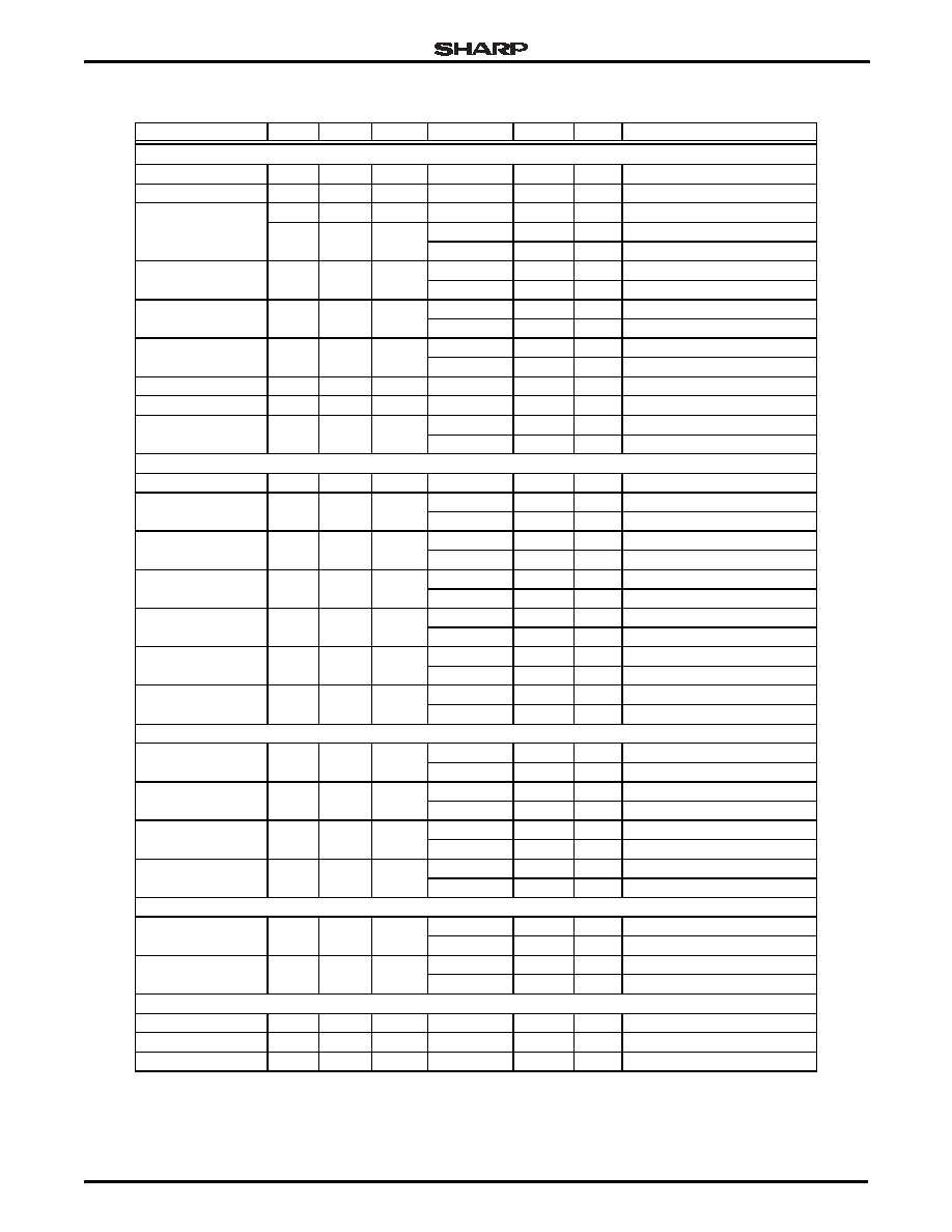
LH7A404
32-Bit System-on-Chip
34
Advance Data Sheet
NOTES:
1. TBD = To Be Determined, awaiting characterization.
2. For Output Drive strength specifications, refer to `DC Specifications'.
SYNCHRONOUS MEMORY INTERFACE SIGNALS
A[15:2]/SA[13:0]
Output
50 pF
8 mA
tOVA
8 ns
Address Valid
A[17:16]/SBANK[1:0]
Output
50 pF
8 mA
tOVB
8 ns
Address Valid/Bank Select Valid
D[31:0]
Output
50 pF
8 mA
tOVD
2 ns
6 ns
Data Valid
Input
tISD
4 ns
Data Setup
tIHD
0 ns
Data Hold
nCAS
Output
30 pF
8 mA
tOVCA
2 ns
6 ns
CAS Valid
tOHCA
0 ns
CAS Hold
nRAS
Output
30 pF
8 mA
tOVRA
2 ns
6 ns
RAS Valid
tOHRA
0 ns
RAS Hold
nSWE
Output
30 pF
8 mA
tOVSDW
2 ns
6 ns
Write Enable Valid
tOHSDW
0 ns
Write Enable Hold
SCKE[1:0]
Output
30 pF
8 mA
tOVC0
2 ns
6 ns
Clock Enable Valid
DQM[3:0]
Output
30 pF
8 mA
tOVDQ
2 ns
6 ns
Data Mask Valid
nSCS[3:0]
Output
30 pF
8 mA
tOVSC
2 ns
6 ns
Synchronous Chip Select Valid
tOVHSC
0 ns
Synchronous Chip Select Hold
PC CARD (PCMCIA) INTERFACE SIGNALS
A[25:0]
Output
50 pF
8 mA
tOVA
8 ns
Address Valid
nCFREG
Output
30 pF
8 mA
tOVDREG
2 ns
8 ns
nREG Valid
tOHDREG
0 ns
nREG Hold
D[31:0]
Input
tISD
4 ns
Data Setup Time
tIHD
0 ns
Data Hold Time
nCFCE1
Output
30 pF
8 mA
tOVCE1
0 ns
8 ns
Chip Enable 1 Valid
tOHCE1
0 ns
Chip Enable 1 Hold
nCFCE2
Output
30 pF
8 mA
tOVCE2
0 ns
8 ns
Chip Enable 2 Valid
tOHCE2
0 ns
Chip Enable 2 Hold
nCFOE
Output
30 pF
8 mA
tOVOE
0 ns
8 ns
Output Enable Valid
tOHOE
0 ns
Output Enable Hold
nCFWE
Output
30 pF
8 mA
tOVWE
0 ns
8 ns
Write Enable Valid
tOHWE
0 ns
Write Enable Hold
MMC INTERFACE SIGNALS
MMCCMD
Output
100 pF
8 mA
tOVCMD
TBD
MMC Command Valid
tOHCMD
TBD
MMC Command Hold
MMCDATA
Output
100 pF
8 mA
tOVDAT
TBD
MMC Data Valid
tOHDAT
TBD
MMC Data Hold
MMCDATA
Input
tISDAT
TBD
MMC Data Setup
tIHDAT
TBD
MMC Data Hold
MMCCMD
Input
tOVCMD
TBD
MMC Command Setup
tIHCMD
TBD
MMC Command Hold
AC97 INTERFACE SIGNALS
AC97OUT
Output
30 pF
8 mA
tOVAC97
TBD
AC97 Output Valid
tOHAC97
TBD
AC97 Output Hold
AC97IN Input
tISAC97
TBD
AC97 Input Setup
tIHAC97
TBD
AC97 Input Hold
SYNCHRONOUS SERIAL PORT (SSP)
SSPFRM
Input
tISSSPFRM
14 ns
SSPFRM Input Valid
SSPTX
Output
50 pF
2 mA
tOVSSPOUT
TBD
SSP Transmit Valid
SSPRX
Input
tISSSPIN
14 ns
SSP Receive Setup
Table 5. AC Signal Characteristics (Cont'd)
SIGNAL
TYPE
LOAD
DRIVE
SYMBOL
MIN.
MAX.
DESCRIPTION
32-Bit System-on-Chip
LH7A404
Advance Data Sheet
35
Asynchronous Memory
Controller Waveforms
Figure 7 shows the waveform and timing for an
external asynchronous memory Write. Figure 8 shows
the waveform and timing for an external asynchronous
memory Read, with one wait state. Figure 9 shows the
waveform and timing for an external asynchronous
memory Read, with two wait states.
Figure 7. External Asynchronous Memory Write
Figure 8. External Asynchronous Memory Read, One Wait State
HCLK
ADDRESS
DATA
A[27:0]
(NOTE 1)
D[31:0]
nCS(X)
nBLE[3:0], nWE
tOVA
tOVD
tOVD
tOHD
tOHCS
tOHBLE
,
tOHWE
tOHA
tOVCS
tOVBLE, tOVWE
LH7A404-10
NOTES:
1. A[24:0] when SCI used.
2. All signal transitions are measured from the
50% point of the clock to the 50% point of the signal.
LH7A404-11
HCLK
ADDRESS
DATA
A[25:0]
D[31:0]
nCSx
nOE
tOVOE
tOVCS
tISD
tOHA
tIHD
tOHCS
tOHOE
tOVA
1 WAIT STATE
DATA READ
NOTE: All signal transitions are measured from the
50% point of the clock to the 50% point of the signal.
LH7A404
32-Bit System-on-Chip
36
Advance Data Sheet
Figure 9. External Asynchronous Memory Read, Two Wait States
LH7A404-12
HCLK
ADDRESS
DATA
A[25:0]
D[31:0]
nCSx
nOE
tOHA
tOHOE
tOHCS
tIHD
tISD
2 WAIT STATES
DATA READ
tOVOE
tOVCS
tOVA
NOTE: All signal transitions are measured from the
50% point of the clock to the 50% point of the signal.

32-Bit System-on-Chip
LH7A404
Advance Data Sheet
37
Synchronous Memory Controller Waveforms
Figure 10 shows the waveform and timing for a Syn-
chronous Burst Read (page already open). Figure 11
shows the waveform and timing for synchronous mem-
ory to activate a bank and Write.
Figure 10. Synchronous Burst Read
Figure 11. Synchronous Bank Activate and Write
tSCLK
LH7A404-13
SA[13:0],
SBANK[1:0]
D[31:0]
NOTES:
1. SDRAMcmd is the combination of nRAS, nCAS, nSDWE, and nSDCSx.
2. tOVXXX represents tOVRA, tOVCA, tOVSDW, or tOVSC.
3. tOHXXX represents tOHRA, tOHCA, tOHSDW, or tOHSC.
4. nDQM is static LOW.
5. SDCKE is static HIGH.
SCLK
SDRAMcmd
tOVXXX
tOVB
tOHXXX
READ
BANK,
COLUMN
tOVA
tISD tIHD
DATA n
DATA n + 1
DATA n + 2
DATA n + 3
LH7A404-14
D[31:0]
SCLK
SDCKE
SDRAMcmd
tSCLK
tOVC0
tOVXXX
tOVA
tOHXXX
tOVA
NOTES:
1. SDRAMcmd is the combination of nRAS, nCAS, nSDWE, and nSDCSx.
2. tOVXXX represents tOVRA, tOVCA, tOVSDW, or tOVSC. Refer to the AC timing table.
3. tOHXXX represents tOHRA, tOHCA, tOHSDW, or tOHSC.
4. nDQM is static LOW.
ACTIVE
WRITE
DATA
BANK,
ROW
BANK,
COLUMN
tOVD
tOHD
SA[13:0],
SBANK[1:0]
LH7A404
32-Bit System-on-Chip
38
Advance Data Sheet
SSP Waveforms
The Synchronous Serial Port (SSP) supports three
data frame formats:
∑ Texas Instruments' synchronous serial
∑ Motorola SPI
∑ National Semiconductor MICROWIRE
Each frame format is between 4 and 16 bits in
length, depending upon the programmed data size.
Each data frame is transmitted beginning with the Most
Significant Bit (MSB) i.e. `big endian'. For all three for-
mats, the SSP serial clock is held LOW (inactive) while
the SSP is idle. The SSP serial clock transitions only
during active transmission of data. The SSPFRM sig-
nal marks the beginning and end of a frame. The
SSPEN signal controls an off-chip line driver's output
enable pin.
Figure 12 and Figure 13 show Texas Instruments
synchronous serial frame format, Figure 14 through
Figure 21 show the Motorola SPI format, and Figure 22
and Figure 23 show National Conductor's MICRO-
WIRE data frame format.
For Texas Instruments' synchronous serial frame for-
mat, the SSPFRM pin is pulsed prior to each frame's
transmission for one serial clock period beginning at its
rising edge. For this frame format, both the SSP and the
external slave device drive their output data on the ris-
ing edge of the clock and latch data from the other
device on the falling edge. See Figure 12 and Figure 13.
Figure 12. Texas Instruments Synchronous Serial Frame Format (Single Transfer)
Figure 13. Texas Instruments Synchronous Serial Frame Format (Continuous Transfer)
LH7A404-24
SSPCLK
SSPFRM
MSB
LSB
SSPTXD/
SSPRXD
4 to 16 BITS
LH7A404-25
SSPCLK
SSPFRM
SSPTXD/
SSPRXD
MSB
LSB
4 to 16 BITS

32-Bit System-on-Chip
LH7A404
Advance Data Sheet
39
For Motorola SPI format, the serial frame pin (SSP-
FRM) is active LOW. The SPO and SPH bits in SSP
Control Register 0 determine SSPCLK and SSPFRM
operation in single and continuous modes. See Figures
14 through 21.
Figure 14. Motorola SPI Frame Format (Single Transfer) with SPO = 0 and SPH = 0
Figure 15. Motorola SPI Frame Format (Continuous Transfer) with SPO = 0 and SPH = 0
Figure 16. Motorola SPI Frame Format (Single Transfer) with SPO = 0 and SPH = 1
LH7A404-26
SSPCLK
nSSPFRM
SSPRXD
MSB
SSPTXD
4 to 16 BITS
MSB
LSB
LSB
Q
NOTE: Q is undefined.
LH7A404-27
SSPCLK
nSSPFRM
SSPTXD/
SSSRXD
4 to 16 BITS
LSB
LSB
MSB
MSB
LH7A404-28
SSPCLK
nSSPFRM
SSPRXD
SSPTXD
NOTE: Q is undefined.
4 to 16 BITS
LSB
LSB
Q
Q
MSB
MSB
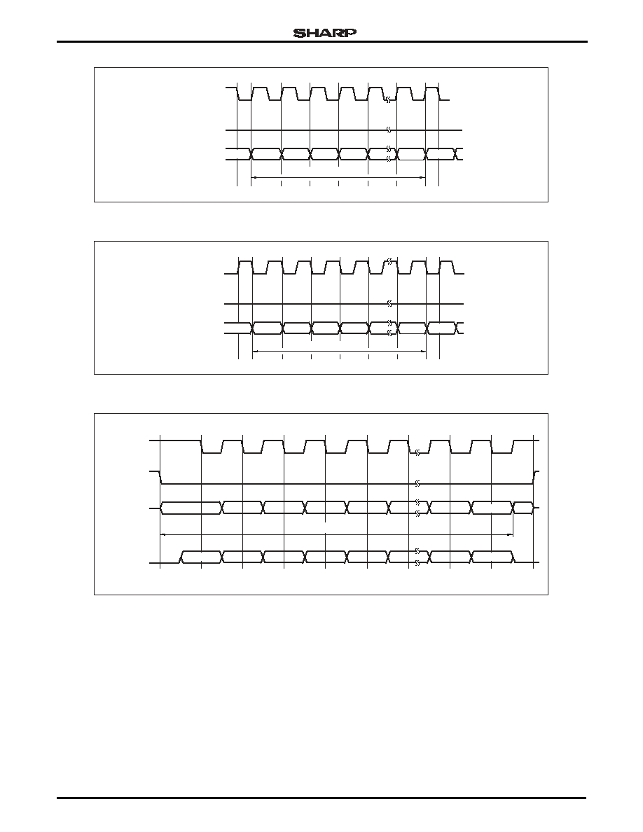
LH7A404
32-Bit System-on-Chip
40
Advance Data Sheet
Figure 17. Motorola SPI Frame Format (Continuous Transfer) with SPO = 0 and SPH = 1
Figure 18. Motorola SPI Frame Format (Continuous Transfer) with SPO = 1 and SPH = 1
Figure 19. Motorola SPI Frame Format (Single Transfer) with SPO = 1 and SPH = 0
LH7A404-29
SSPCLK
nSSPFRM
SSPTXD/
SSSRXD
4 to 16 BITS
LSB
MSB
LSB
MSB
LH7A404-30
SSPCLK
nSSPFRM
SSPTXD/
SSSRXD
4 to 16 BITS
LSB
MSB
LSB
MSB
LH7A404-31
SSPCLK
nSSPFRM
SSPRXD
SSPTXD
NOTE: Q is undefined.
MSB
MSB
LSB
LSB
Q
4 to 16 BITS

32-Bit System-on-Chip
LH7A404
Advance Data Sheet
41
Figure 20. Motorola SPI Frame Format (Continuous Transfer) with SPO = 1 and SPH = 0
Figure 21. Motorola SPI Frame Format (Single Transfer) with SPO = 1 and SPH = 1
LH7A404-32
SSPCLK
nSSPFRM
SSPTXD/
SSPRXD
MSB
LSB
MSB
LSB
4 to 16 BITS
LH7A404-33
SSPCLK
nSSPFRM
SSPRXD
SSPTXD
4 to 16 BITS
MSB
MSB
Q
LSB
LSB
Q
NOTE: Q is undefined.

LH7A404
32-Bit System-on-Chip
42
Advance Data Sheet
For National Semiconductor MICROWIRE format,
the serial frame pin (SSPFRM) is active LOW. Both the
SSP and external slave device drive their output data
on the falling edge of the clock, and latch data from the
other device on the rising edge of the clock. Unlike the
full-duplex transmission of the other two frame formats,
the National Semiconductor MICROWIRE format uti-
lizes a master-slave messaging technique that oper-
ates in half-duplex. When a frame begins in this mode,
an 8-bit control message is transmitted to the off-chip
slave. During this transmission no incoming data is
received by the SSP. After the message has been sent,
the external slave device decodes the message. After
waiting one serial clock period after the last bit of the 8-
bit control message was received it responds by return-
ing the requested data. The returned data can be 4 to
16 bits in length, making the total frame length between
13 to 25 bits. See Figure 22 and Figure 23.
Figure 22. MICROWIRE Frame Format (Single Transfer)
Figure 23. MICROWIRE Frame Format (Continuous Transfers)
LH7A404-34
LSB
MSB
0
LSB
MSB
8-BIT CONTROL
SSPCLK
nSSPFRM
SSPTXD
SSPRXD
4 to 16 BITS
OUTPUT DATA
LH7A404-35
SSPCLK
nSSPFRM
SSPTXD
SSPRXD
4 to 16 BITS
OUTPUT DATA
8-BIT CONTROL
MSB
MSB
LSB
LSB
0
LSB
MSB

32-Bit System-on-Chip
LH7A404
Advance Data Sheet
43
PC Card (PCMCIA) Waveforms
Figure 24 shows the waveforms and timing for a
PCMCIA attribute memory Read transfer, Figure 25
shows the waveforms and timing for a PCMCIA attribute
memory Write transfer, Figure 26 shows the waveforms
and timing for a PCMCIA common memory Read trans-
fer, and Figure 27 shows the waveforms and timing for a
PCMCIA common memory Write transfer.
Figure 24. PCMCIA Attribute Memory Read Transfer
tOVA
tOHA
tOVDREG
HCLK
A[25:0]
nCFREG
nCFCE1
nCFCE2
nCFOE
nCFWE
D[31:0]
tOVCE1
tOHDREG
tOHCE1
tOVOE
tOHOE
tIHD
tISD
D[7:0] (EVEN BYTE)
LH7A404-15

LH7A404
32-Bit System-on-Chip
44
Advance Data Sheet
Figure 25. PCMCIA Attribute Memory Write Transfer
HCLK
A[25:0]
D[7:0] (EVEN BYTE)
tOVA
tOHA
tOVCE1
tOHCE1
tOVWE
tOHWE
tIHD
tISD
LH7A404-16
nCFREG
nCFCE1
nCFCE2
nCFOE
nCFWE
D[31:0]
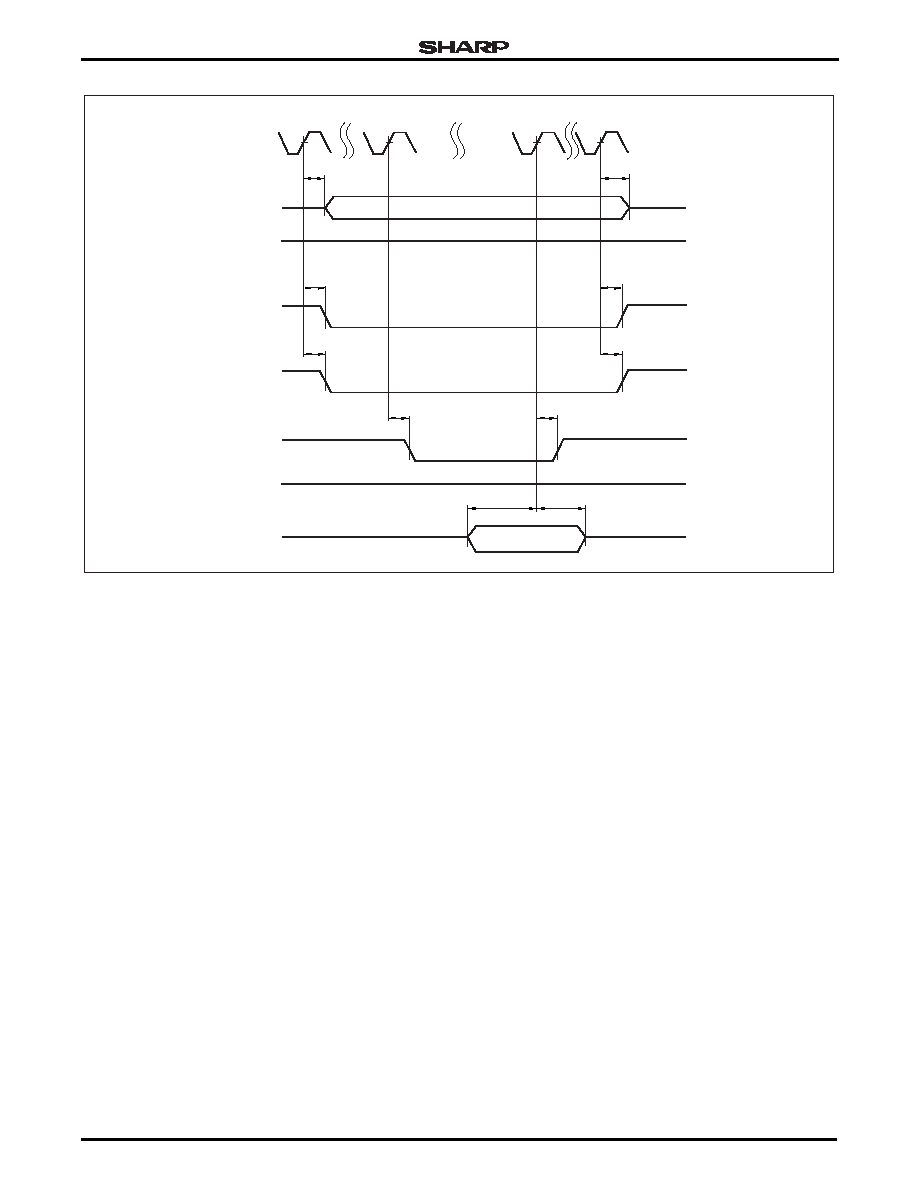
32-Bit System-on-Chip
LH7A404
Advance Data Sheet
45
Figure 26. PCMCIA Common Memory Read Transfer
tOVA
tOHA
tOVCE1
HCLK
A[25:0]
tOVCE2
tOHCE1
tOHCE2
tOVOE
tOHOE
tIHD
tISD
D[15:0] (WORD)
LH7A404-17
nCFREG
nCFCE1
nCFCE2
nCFOE
nCFWE
D[31:0]
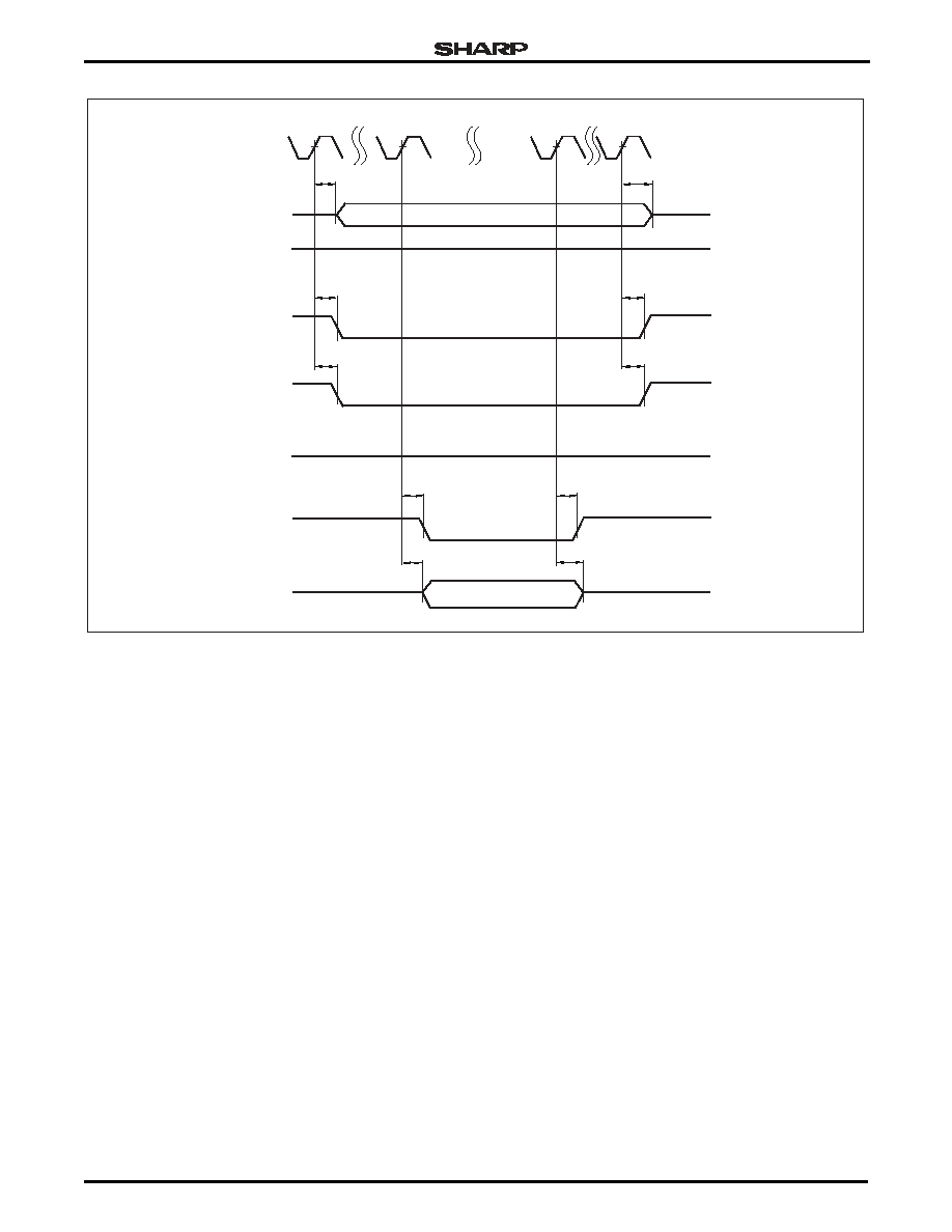
LH7A404
32-Bit System-on-Chip
46
Advance Data Sheet
Figure 27. PCMCIA Common Memory Write Transfer
tOVA
tOHA
tOVCE1
HCLK
A[25:0]
tOVCE2
tOHCE1
tOHCE2
tOVOE
tOHOE
tIHD
tISD
D[15:0] (WORD)
LH7A404-18
nCFREG
nCFCE1
nCFCE2
nCFOE
nCFWE
D[31:0]

32-Bit System-on-Chip
LH7A404
Advance Data Sheet
47
MMC Interface Waveforms
Figure 28 shows the waveforms and timing for an
MMC command or data Write. Figure 29 shows the
waveforms and timing for an MMC command or data
Read.
AC97 Interface Waveforms
Figure 30 shows the waveforms and timing for the
AC97 interface Data Setup and Hold.
Figure 28. MMC Command/Data Write
Figure 29. MMC Command/Data Read
Figure 30. AC97 Data Setup and Hold
tOVCMD
MMCCLK
MMCCMD
MMCDAT
tOHCMD
tOVDAT
tOHDAT
LH7A404-19
tIOVCMD
MMCCLK
MMCCMD
MMCDAT
tIHCMD
tISDAT tIHDAT
LH7A404-20
tOVAC97
AC97SYNC
AC97OUT
AC97IN
tISAC97 tIHAC97
tOHAC97
LH7A404-21

LH7A404
32-Bit System-on-Chip
48
Advance Data Sheet
Reset, Clock, and Power Controller
(RCPC) Waveforms
Figure 31 shows the behavior of the LH7A404 when
coming out of Reset or Power-On. Figure 32 shows
external reset timing, and Table 6 gives the timing
parameters.
NOTE: *VDDC = VDDCmin
Table 6. Reset AC Timing
PARAMETER
DESCRIPTION
MIN.
TYP.
MAX.
UNIT
tOSC (32 kHz)
Oscillator stabilization time after Power Up (VDDC = VDDCMIN)
550
ms
tOSC (14 MHz)
Oscillator stabilization time after Power Up (VDDC = VDDCMIN)
2.5
ms
tRSTIW
nRESETIN Pulse Width (once sampled LOW)
2
HCLK
tRSTOV
nRESETIN LOW to nRESETOUT valid (once nRESETIN sampled LOW)
3.5
HCLK
tRSTOH
nRESETOUT hold relative to nRESETIN HIGH
1
HCLK
Figure 31. PLL Start-up
Figure 32. External Reset
LH7A404-22
tOSC
VDDC
VDDCmin
XTAL
nRESETI
LH7A404-23
tRSTIW
nRESETI

32-Bit System-on-Chip
LH7A404
Advance Data Sheet
49
DC/AC SPECIFICATIONS (INDUSTRIAL)
To be determined.

LH7A404
32-Bit System-on-Chip
50
Advance Data Sheet
PACKAGE SPECIFICATIONS
Figure 33. 324-Ball PBGA Package Specification
1.00 REF.
1.00
19.50
+0.70
-0.05
19.50
+0.70
-0.05
+0.07
-0.13
7.35
5.17
7.35
5.17
16.15 MAX.
16.15 MAX.
SIDE VIEW
TOP VIEW
BOTTOM VIEW
(324 solder balls)
1.00 REF
.
0.50 R,
3 PLACES
NOTE: Dimensions in mm.
Z
C A
C
B
0.30 M
0.63
0.10 M
Z
0.15
1.17 ±0.05
0.50 ±0.10
2.23 ±0.21
SEATING PLANE
0.56 ±0.06
B
A1 BALL
PAD CORNER
15
13
11
9
7
5
20 19 17
3
A
B
C
D
E
F
G
H
J
K
L
M
N
P
R
T
U
V
W
Y
AA
AB
1
16
30
∞
TYP.
14
12
10
22
20
18
8
6
4
2
A
(4X)
0.20
Z
0.25
Z
0.35
23.00
23.00
324-BALL PBGA
A1 BALL
PAD
CORNER
A1 BALL PAD
INDICATOR, 1.0 DIA.
AVAILABLE
MARKING
AREA
45
∞
CHAMFER
4 PLACES
324PBGA

LH7A404
32-Bit System-on-Chip
©2002 by SHARP Corporation
Reference Code SMA02004
SPECIFICATIONS ARE SUBJECT TO CHANGE WITHOUT NOTICE.
Suggested applications (if any) are for standard use; See Important Restrictions for limitations on special applications. See Limited
Warranty for SHARP's product warranty. The Limited Warranty is in lieu, and exclusive of, all other warranties, express or implied.
ALL EXPRESS AND IMPLIED WARRANTIES, INCLUDING THE WARRANTIES OF MERCHANTABILITY, FITNESS FOR USE AND
FITNESS FOR A PARTICULAR PURPOSE, ARE SPECIFICALLY EXCLUDED. In no event will SHARP be liable, or in any way responsible,
for any incidental or consequential economic or property damage.
NORTH AMERICA
EUROPE
JAPAN
SHARP Microelectronics of the Americas
5700 NW Pacific Rim Blvd.
Camas, WA 98607, U.S.A.
Phone: (1) 360-834-2500
Fax: (1) 360-834-8903
www.sharpsma.com
SHARP Microelectronics Europe
Division of Sharp Electronics (Europe) GmbH
Sonninstrasse 3
20097 Hamburg, Germany
Phone: (49) 40-2376-2286
Fax: (49) 40-2376-2232
www.sharpsme.com
SHARP Corporation
Electronic Components & Devices
22-22 Nagaike-cho, Abeno-Ku
Osaka 545-8522, Japan
Phone: (81) 6-6621-1221
Fax: (81) 6117-725300/6117-725301
www.sharp-world.com
TAIWAN
SINGAPORE
KOREA
SHARP Electronic Components
(Taiwan) Corporation
8F-A, No. 16, Sec. 4, Nanking E. Rd.
Taipei, Taiwan, Republic of China
Phone: (886) 2-2577-7341
Fax: (886) 2-2577-7326/2-2577-7328
SHARP Electronics (Singapore) PTE., Ltd.
438A, Alexandra Road, #05-01/02
Alexandra Technopark,
Singapore 119967
Phone: (65) 271-3566
Fax: (65) 271-3855
SHARP Electronic Components
(Korea) Corporation
RM 501 Geosung B/D, 541
Dohwa-dong, Mapo-ku
Seoul 121-701, Korea
Phone: (82) 2-711-5813 ~ 8
Fax: (82) 2-711-5819
CHINA
HONG KONG
SHARP Microelectronics of China
(Shanghai) Co., Ltd.
28 Xin Jin Qiao Road King Tower 16F
Pudong Shanghai, 201206 P.R. China
Phone: (86) 21-5854-7710/21-5834-6056
Fax: (86) 21-5854-4340/21-5834-6057
Head Office:
No. 360, Bashen Road,
Xin Development Bldg. 22
Waigaoqiao Free Trade Zone Shanghai
200131 P.R. China
Email: smc@china.global.sharp.co.jp
SHARP-ROXY (Hong Kong) Ltd.
3rd Business Division,
17/F, Admiralty Centre, Tower 1
18 Harcourt Road, Hong Kong
Phone: (852) 28229311
Fax: (852) 28660779
www.sharp.com.hk
Shenzhen Representative Office:
Room 13B1, Tower C,
Electronics Science & Technology Building
Shen Nan Zhong Road
Shenzhen, P.R. China
Phone: (86) 755-3273731
Fax: (86) 755-3273735