 | –≠–ª–µ–∫—Ç—Ä–æ–Ω–Ω—ã–π –∫–æ–º–ø–æ–Ω–µ–Ω—Ç: LR38630 | –°–∫–∞—á–∞—Ç—å:  PDF PDF  ZIP ZIP |
Document Outline
- ˛ˇ
- ˛ˇ
- ˛ˇ
- ˛ˇ
- ˛ˇ
- ˛ˇ
- ˛ˇ
- ˛ˇ
- ˛ˇ
- ˛ˇ

DESCRIPTION
The LR38630 is a CMOS digital signal processor
for color camera systems of 110 k-pixel CMOS
image sensor with primary color mosaic filters. The
camera system consists of CIF CMOS image
sensor (LZ34C10) and DSP IC (LR38630) with 2 k-
bit EEPROM. Depending on application, 1 M-bit
SRAM can be added in order to get slower frame
rate at video output.
FEATURES
∑ Designed for 110 k-pixel color CMOS image
sensors with R, G, and B color mosaic filters
∑ Compatible with CIF standard
∑ External control interface input/output
∑ Variable GAMMA and KNEE response
∑ 8-bit digital input
∑ Available for digital video 4 : 2 : 2 (U/Y/V/Y)
output
∑ Built-in synchronous signal generation circuit to
drive CMOS image sensor
∑ Built-in 2 k-bit EEPROM controller to set the
camera adjustment data
∑ Built-in auto exposure control
∑ Built-in auto white balance control
∑ Built-in auto carrier balance control
∑ Built-in white blemish compensator
∑ Lower power consumption by dual clocking signal
process technology
∑ Single +3.0 V power supply
∑ Package :
80-pin LQFP (LQFP080-P-1212) 0.5 mm pin-pitch
LR38630
LR38630
Digital Signal Processor for
CIF CMOS Image Cameras
In the absence of confirmation by device specification sheets, SHARP takes no responsibility for any defects that may occur in equipment using any SHARP devices shown in
catalogs, data books, etc. Contact SHARP in order to obtain the latest device specification sheets before using any SHARP device.
1

LR38630
2
PIN CONNECTIONS
ACL
CKI
GND
V
DD
AD
7
AD
6
AD
5
AD
4
AD
3
AD
2
AD
1
AD
0
GND
V
DD
TST
3
ADDSEL
SCLK
SDI
CHD
CVD
DATA
4
DATA
5
DATA
6
DATA
7
RCLK
V
DD
GND
EXMCK
MDIO
0
MDIO
1
MDIO
2
MDIO
3
MDIO
4
MDIO
5
MDIO
6
MDIO
7
WE
OE
TST
2
TST
1
ADJMODE
IFMODE
EEPCK
EEPDA
V
DD
GND
VS
OLSTEN
HREF
STANDBY
CTLDCK
CTLDEN
CTLDOUT
CTLDIN
V
DD
GND
DATA
0
DATA
1
DATA
2
DATA
3
ADD
16
ADD
15
ADD
14
GND
V
DD
ADD
13
ADD
12
ADD
11
ADD
10
ADD
9
ADD
8
ADD
7
ADD
6
GND
ADD
5
ADD
4
ADD
3
ADD
2
ADD
1
ADD
0
21
22
23
24
25
26
27
28
29
30
31
32
33
34
35
36
37
38
39
40
80
79
78
77
76
75
74
73
72
71
70
69
68
67
66
65
64
63
62
61
1
2
3
4
5
6
7
8
9
10
11
12
13
14
15
16
17
18
19
20
60
59
58
57
56
55
54
53
52
51
50
49
48
47
46
45
44
43
42
41
80-PIN LQFP
TOP VIEW
(LQFP080-P-1212)

BLOCK DIAGRAM
LR38630
3
OE, WE
EXMCK
DATA
7-
DATA
0
RCLK
CTLDIN, CTLDOUT
CTLDEN, CTLDCK
IFMODE, ADJMODE
EEPDA, EEPCK
HREF, OLSTEN,
VS
FPN
SUPPRESSION
EXTERNAL
INTERFACE
EEPROM
INTERFACE
PROCESSOR
SSG
SRAM
CONTROL
BLACK
BALANCE
EXPOSURE
CONTROL
COLOR
MATRIX
COLOR
SUPPRESS
WHITE
BALANCE
INTER-
POLATION
GAMMA
SETUP
1H/2H
DELAY
LINE
WHITE
BALANCE
CONTROL
CMOS
IMAGE
SENSOR
INTERFACE
IMAGE
FORMAT
CONVERTER
CMOS
IMAGE
SENSOR
SSG
LUMINANCE
SIGNAL
PROCESS
OB CLAMP
MDIO
7-
MDIO
0
ADD
16-
ADD
0
AD
7-
AD
0
SDI, SCLK
CVD, CHD
ACL
CKI
STANDBY
TST
1
, TST
2

4
LR38630
PIN DESCRIPTION
PIN NO. SYMBOL
I/O
POLARITY
DESCRIPTION
1
ACL
IC
Initializing input.
2
CKI
IC
Clock input. Connect to pin 14 of LZ34C10.
Digital signal input, fed from pin 19 of LZ34C10.
IC
AD
3
9
Digital signal input, fed from pin 20 of LZ34C10.
IC
AD
4
8
Digital signal input, fed from pin 21 of LZ34C10.
IC
AD
5
7
Digital signal input, fed from pin 22 of LZ34C10.
IC
AD
6
6
Digital signal input, fed from pin 23 of LZ34C10 (MSB).
IC
AD
7
5
Supply of +3.0 V power.
≠
V
DD
4
A grounding pin.
≠
GND
3
12
AD
0
IC
Digital signal input, fed from pin 16 of LZ34C10 (LSB).
11
AD
1
IC
Digital signal input, fed from pin 17 of LZ34C10.
10
AD
2
IC
Digital signal input, fed from pin 18 of LZ34C10.
Clock output of serial data, connected to pin 28 of LZ34C10.
OBF4M
SCLK
17
Pin to set MSB to be added on serial address data.
Low : MSB = 0 (address 00h-7Fh),
High : MSB = 1 (address 80h-FFh)
IC
ADDSEL
16
A test pin. Connect to GND.
IC
TST
3
15
Supply of +3.0 V power.
≠
V
DD
14
A grounding pin.
≠
GND
13
18
SDI
OBF4M
Serial data output, connected to pin 27 of LZ34C10.
Vertical drive pulse output, connected to pin 26 of LZ34C10.
OBF4M
CVD
20
Horizontal drive pulse output, connected to pin 25 of LZ34C10.
OBF4M
CHD
19
21
ADD
16
OBF4M
Address output to drive an external SRAM.
A grounding pin.
≠
GND
24
Address output to drive an external SRAM.
OBF4M
ADD
14
23
Address output to drive an external SRAM.
OBF4M
ADD
15
22
28
ADD
11
OBF4M
Address output to drive an external SRAM.
27
ADD
12
OBF4M
Address output to drive an external SRAM.
26
ADD
13
OBF4M
Address output to drive an external SRAM.
25
V
DD
≠
Supply of +3.0 V power.
Address output to drive an external SRAM.
IO4M
ADD
7
32
Address output to drive an external SRAM.
IO4M
ADD
8
31
Address output to drive an external SRAM.
IO4M
ADD
9
30
Address output to drive an external SRAM.
IO4M
ADD
10
29
35
ADD
5
IO4M
Address output to drive an external SRAM.
34
GND
≠
A grounding pin.
33
ADD
6
IO4M
Address output to drive an external SRAM.
36
ADD
4
IO4M
Address output to drive an external SRAM.
Address output to drive an external SRAM.
IO4M
ADD
1
39
Address output to drive an external SRAM.
IO4M
ADD
2
38
Address output to drive an external SRAM.
IO4M
ADD
3
37
LR38630
5
PIN NO. SYMBOL
I/O
POLARITY
DESCRIPTION
Write enable to drive an external SRAM.
OBF4M
WE
44
Output enable to drive an external SRAM.
OBF4M
OE
43
A test pin. Connected to GND.
IC
TST
2
42
A test pin. Connected to GND.
IC
TST
1
41
Address output to drive an external SRAM.
IO4M
ADD
0
40
52
MDIO
0
IO4MU
Address output to drive an external SRAM.
51
MDIO
1
IO4MU
Address output to drive an external SRAM.
50
IO4MU
Address output to drive an external SRAM.
49
MDIO
3
IO4MU
Address output to drive an external SRAM.
48
MDIO
4
IO4MU
Address output to drive an external SRAM.
47
MDIO
5
IO4MU
Address output to drive an external SRAM.
46
MDIO
6
IO4MU
Address output to drive an external SRAM.
45
MDIO
7
IO4MU
Address output to drive an external SRAM.
MDIO
2
Data input/output to drive an external SRAM.
OBF4M
DATA
7
57
Clock output for digital video output signal.
OBF4M
RCLK
56
Supply of +3.0 V power.
≠
V
DD
55
A grounding pin.
≠
GND
54
External clock input.
IC
EXMCK
53
63
DATA
1
OBF4M
Data input/output to drive an external SRAM.
62
DATA
2
OBF4M
Data input/output to drive an external SRAM.
61
DATA
3
OBF4M
Data input/output to drive an external SRAM.
60
DATA
4
OBF4M
Data input/output to drive an external SRAM.
59
DATA
5
OBF4M
Data input/output to drive an external SRAM.
58
DATA
6
OBF4M
Data input/output to drive an external SRAM.
High level puts this IC and LZ34C10 in standby mode.
IC
STANDBY
71
Clock input to set the data.
IC
CTLDCK
70
The rising edge enables the serial data to be available.
IC
CTLDEN
69
Serial data input.
OBF4M
CTLDOUT
68
Serial data input.
IC
CTLDIN
67
Supply of +3.0 V power.
≠
V
DD
66
A grounding pin.
≠
GND
65
Data input/output to drive an external SRAM.
OBF4M
DATA
0
64
73
OLSTEN OBF4M
Horizontal pulse output going to low level when starting in horizontal.
72
HREF
OBF4M
Horizontal blanking pulse output keeping high level during the effective image
period.
74
VS
OBF4M
Vertical blanking pulse output keeping high level during the effective image
period.
Supply of +3.0 V power.
≠
V
DD
76
A grounding pin.
≠
GND
75
77
EEPDA
IO4M
Data input/output to/from EEPROM.
Going to high-impedance with high level of pin 80.

6
LR38630
PIN NO. SYMBOL
I/O
POLARITY
DESCRIPTION
Clock input/output to/from EEPROM.
Going to high-impedance with high level of pin 80.
IO4M
EEPCK
78
The option of number of bits of serial data to adjust.
High level : W/R flag + address 6 bits + data 16 bits
Low level : W/R flag + address 8 bits + data 8 bits
IC
IFMODE
79
80
ADJMODE
IC
Void input of internal automatic control circuit, connected to low level normally.
High level input stops automatic control function.
Power-on with high level input stops automatic loading of EEPROM data.
IO4M
: Input/output pin (4 mA output, CMOS level input)
IO4MU
: Input/output pin (4 mA output, CMOS level input
with pull-up resistor)
OBF4M
: Output pin (4 mA output)
IC
: Input pin (CMOS level input)

LR38630
7
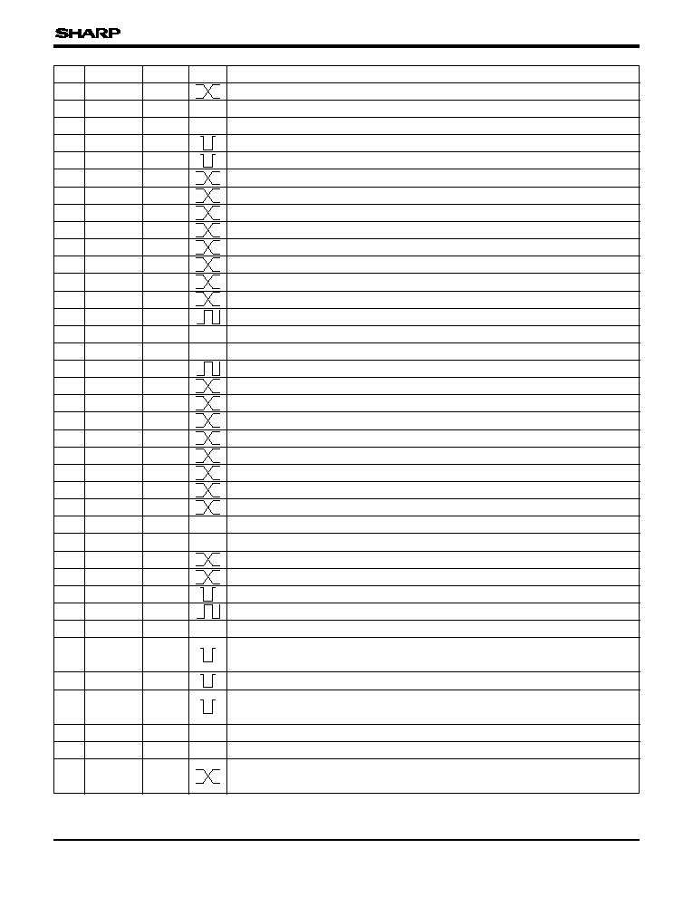
INTERNAL COEFFICIENT TABLE
ADDRESS
NAME
BITS
FUNCTION
≠
00h
≠
Not used.
Option of the output image type.
00 : Normal
01 : Inverted top and bottom
10 : Reversed left and right
11 : Reversed all
MOS_MIR
02h
2
(7)
(6)
Not used.
≠
01h
≠
1
(0)
MOS_STD
Under low level at pin 71, this bit can make CMOS image sensor standby.
0 : Operating
1 : Standby
3
(3)
(2)
(1)
MOS_AGC
Option of AGC offset gain.
000 : 3 dB
001 : 4 dB
010 : 5 dB
011 : 6 dB
100 : 7 dB
101 : 8 dB
110 : 9 dB
111 : 10 dB
Option of AD converter clock phase.
00 : Reference
01 : Delayed by 90∞
10 : Delayed by 180∞
11 : Delayed by 270∞
MOS_SAD
2
(5)
(4)
Option of electronic exposure mode.
00 : Automatic electronic shutter speed and AGC ON
01 : Fixed electronic shutter speed and AGC ON
10 : Automatic electronic shutter speed and AGC OFF
11 : Fixed electronic shutter speed and AGC OFF
EE_HOLD
2
(2)
(1)
Option of white balance mode.
00 : Automatic
01 : Preset WB1
1X : Preset WB2
WB_MODE
2
(4)
(3)
Option of exposure level reference.
0 : Data of address 06h
1 : Data of address 09h
BLC
1
(5)
Option of sampling position in QCIF.
0 : Red filter
1 : Green filter
QCIF_SEL
1
(7)
1
(6)
CA_HOLD
Carrier balance function.
0 : Automatic added an offset (coefficient)
1 : 0h added an offset (coefficient)
03h
1
(0)
OFSET_AUTO
Option of optical black level control.
0 : Automatic
1 : Fixed level

8
LR38630
ADDRESS
NAME
BITS
FUNCTION
Option of output mode.
00 : QCIF1
01 : CIF
10 : QVGA
11 : QCIF2
OUT_SEL
04h
2
(7)
(6)
4
(3)
(2)
(1)
(0)
ACT_MODE
0000 : CIF image output with CKI clock of CMOS image sensor
0001 : 1 frame of image output per second with CKI clock
0010 : 2 frames of image output per second with CKI clock
0011 : 15 frames of image output per second with CKI clock
0101 : 1 frame of image output per second with EXCK clock
(1 frame data is written to RAM in vertical blanking.)
0110 : 2 frames of image output per second with EXCK clock
(2 frames data are written to RAM in vertical blanking.)
0111 : Image output with EXMCK clock
(EXMCK should be lower than 4.5 MHz.)
1XXX : Except 0000, works with 30 frames after power-on.
(example) 1001 : 1 frame of image output per second with CKI starting
with 30 frames after power-on.
1000 : Prohibited to use
Clock timing for input.
00 : Delayed by one CK
01 : Delayed by two CK
10 : Not delayed
IN_TIM
2
(5)
(4)
Setting a period to work with 30 frames after power-on.
A period = (Data + 1) x frame rate
ACT_TIM
8
05h
09h
8
REF_BLC
Exposure reference level in BLC (valid with BLC of address 03h = 1).
08h
8
CTLD_02
The first target area of electronic exposure control.
If exposure control data is over (data of address 06h ± data of address 08h), the
exposure control is restarted.
07h
8
CTLD_01
The second target area of electronic exposure control.
In the case that exposure control data is within (data of address 06h ± data of
address 07h), the exposure control is completed.
06h
8
REF_IRIS
Electronic exposure reference level.
The first target area of electronic exposure control in BLC.
If exposure control data is over (data of address 09h ± data of address 0Bh), the
exposure control is restarted.
CTLD_12
8
0Bh
The second target area of electronic exposure control in BLC.
In the case that exposure control data is within (data of address 09h ± data of
address 0Ah), the exposure control is completed.
CTLD_11
8
0Ah

LR38630
9
ADDRESS
NAME
BITS
FUNCTION
Option of maximum electronic shutter speed in automatic.
Electronic exposure control.
00 : 1/9 900 s
01 : 1/4 950 s
10 : 1/1 980 s
11 : 1/1 100 s
SH_MAX
0Ch
2
(7)
(6)
2
(3)
(2)
EE_RATIO
Window option of automatic electronic exposure control.
00 : Center weighted 1
01 : Center weighted 2
10 : No window
11 : Lower-position weighted
Option of electronic shutter speed and AGC speed change.
00 : Shutter speed is changed by 10-19 pitches.
01 : Shutter speed is changed by 8-10 pitches.
1X : Shutter speed is changed by 1 pitch (the finest)
EE_SPD
2
(5)
(4)
Option of time constant in electronic exposure control.
00 : Longer time constant 01 : Long time constant
1X : No time constant
EE_LPF
2
(1)
(0)
1
SH_HOLD2
MSB of fixed electronic shutter speed.
0Dh
0Fh
Preset gain in making AGC OFF (EE_HOLD = 1X at address 03h).
AGC_HOLD
8
0Eh
Lower bits of fixed electronic shutter speed.
Data between 000 and 149 can be set by address 0Dh and 0Eh.
SH_HOLD1
8
8
OFSET_HOLD
Fixed optical black level (OFSET_AUTO =1 at address 03h).
10h
Time constant option of automatic optical black level control.
00 : Longer time constant
01 : Long time constant
1X : No time constant
OFSET_LPF
2
(4)
(3)
2
(1)
(0)
SEL_LPF
Time constant option of automatic white balance control.
00 : Longer time constant
01 : Long time constant
1X : No time constant
1
(2)
WBFIX1
Option of automatic white balance control.
0 : Not accelerated 1 : Accelerated
11h
The first target area of automatic white balance control in minus direction of high-
speed mode.
In the case that white balance control data is within (data of address 12h + data of
address 13h), high-speed mode control is completed and then changed to normal-
speed control mode.
KGBGR1
8
12h

LR38630
10
ADDRESS
NAME
BITS
FUNCTION
The first target area of automatic white balance control in plus direction of high-
speed mode.
In the case that white balance control data is within (data of address 12h + data of
address 13h), high-speed mode control is completed and then changed to normal-
speed control mode.
KGBGR2
8
13h
16h
8
LIMIM
Limitation in making white balance data at minus I-axis.
15h
8
KGBGR4
The second target area of automatic white balance control in plus direction of high-
speed mode.
In the case that white balance control data is over (data of address 14h + data of
address 15h), high-speed mode control is restarted.
14h
8
KGBGR3
The second target area of automatic white balance control in minus direction of
high-speed mode.
In the case that white balance control data is over (data of address 14h + data of
address 15h), high-speed mode control is restarted.
Limitation in making white balance data at plus Q-axis.
LIMQP
8
19h
Limitation in making white balance data at minus Q-axis.
LIMQM
8
18h
Limitation in making white balance data at plus I-axis.
LIMIP
8
17h
1Bh
8
YHCL
Limitation in making white balance data. A pixel with higher luminance level than
data of this address is neglected.
1Ah
8
YLCL
Limitation in making white balance data. A pixel with lower luminance level than
data of this address is neglected.
The first target area of auto white balance control in plus I-axis.
LIMWIIP
7
1Dh
The first target area of auto white balance control in minus I-axis. In the case that
white balance control data is within the area by address 1Ch, 1Dh, 1Eh and 1Fh,
automatic white balance control is completed.
LIMWIIM
7
1Ch
1Fh
7
LIMWIQP
The first target area of auto white balance control in plus Q-axis.
1Eh
7
LIMWIQM
The first target area of auto white balance control in minus Q-axis.
20h
7
LIMWOI
The second target area of auto white balance control in I-axis. In the case that
white balance control data is over the area by address 20h and 21h, automatic
white balance control is restarted.
The second target area of auto white balance control in Q-axis. In the case that
white balance control data is over the area by address 20h and 21h, automatic
white balance control is restarted.
LIMWOQ
7
21h
Maximum gain of red signal in automatic white balance control.
WBR_MAX
8
22h
29h
8
WBB2
White balance preset 2 : Blue signal gain
28h
8
WBR2
White balance preset 2 : Red signal gain
27h
8
WBB1
White balance preset 1 : Blue signal gain
26h
8
WBR1
White balance preset 1 : Red signal gain
25h
8
WBB_MIN
Minimum gain of blue signal in automatic white balance control.
24h
8
WBB_MAX
Maximum gain of blue signal in automatic white balance control.
23h
8
WBR_MIN
Minimum gain of red signal in automatic white balance control.

LR38630
11
ADDRESS
NAME
BITS
FUNCTION
2Ch
8
GAM_SLOPE2
Gamma curve setting : Third straight line slope
2Bh
8
GAM_SLOPE1
Gamma curve setting : Second straight line slope
2Ah
8
GAM_SLOPE0
Gamma curve setting : First straight line slope
Gamma curve setting : Tenth straight line slope
GAM_SLOPE9
8
33h
Gamma curve setting : Ninth straight line slope
GAM_SLOPE8
8
32h
Gamma curve setting : Eighth straight line slope
GAM_SLOPE7
8
31h
Gamma curve setting : Seventh straight line slope
GAM_SLOPE6
8
30h
Gamma curve setting : Sixth straight line slope
GAM_SLOPE5
8
2Fh
Gamma curve setting : Fifth straight line slope
GAM_SLOPE4
8
2Eh
Gamma curve setting : Fourth straight line slope
GAM_SLOPE3
8
2Dh
3Bh
8
GAM_OFSET8
Gamma curve setting : Ninth straight line offset
3Ah
8
GAM_OFSET7
Gamma curve setting : Eighth straight line offset
39h
8
GAM_OFSET6
Gamma curve setting : Seventh straight line offset
38h
8
GAM_OFSET5
Gamma curve setting : Sixth straight line offset
37h
8
GAM_OFSET4
Gamma curve setting : Fifth straight line offset
36h
8
GAM_OFSET3
Gamma curve setting : Fourth straight line offset
35h
8
GAM_OFSET2
Gamma curve setting : Third straight line offset
34h
8
GAM_OFSET1
Gamma curve setting : Second straight line offset
Horizontal aperture gain.
KHGA
8
43h
Horizontal aperture level compression in lower luminance level.
KHC
6
42h
Gain in middle frequency components of luminance signal.
KY1
8
41h
Carrier balance : Green signal compensation in BG line
KCBG2
8
40h
Carrier balance : Green signal compensation in RG line
KCBG1
8
3Fh
Carrier balance : Blue signal compensation
KCBB
8
3Eh
Carrier balance : Red signal compensation
KCBR
8
3Dh
Gamma curve setting : Tenth straight line offset
GAM_OFSET9
8
3Ch
49h
8
K1_MAT1
AWB color matrix : R ≠ Y 2
48h
8
K0_MAT1
AWB color matrix : R ≠ Y 1
47h
6
KSU
Set up level.
46h
8
KLL
Luminance level.
45h
8
KVGA
Vertical aperture gain.
44h
6
KVC
Vertical aperture level compression in lower luminance level.
AWB color matrix : B ≠ Y 1
K2_MAT1
8
4Ah
4Bh
8
K3_MAT1
AWB color matrix : B ≠ Y 2
WB1 color matrix : R ≠ Y 2
K1_MAT2
8
4Dh
52h
8
K2_MAT3
WB2 color matrix : B ≠ Y 1
51h
8
K1_MAT3
WB2 color matrix : R ≠ Y 2
50h
8
K0_MAT3
WB2 color matrix : R ≠ Y 1
4Fh
8
K3_MAT2
WB1 color matrix : B ≠ Y 2
4Eh
8
K2_MAT2
WB1 color matrix : B ≠ Y 1
WB1 color matrix : R ≠ Y 1
K0_MAT2
8
4Ch

LR38630
12
ADDRESS
NAME
BITS
FUNCTION
57h
8
KCBGA1
WB1 color level : B ≠ Y
56h
8
KCRGA1
WB1 color level : R ≠ Y
55h
8
KCBGA
AWB color level : B ≠ Y
54h
8
KCRGA
AWB color level : R ≠ Y
53h
8
K3_MAT3
WB2 color matrix : B ≠ Y 2
Gain to suppress color signal level by data of address 61h.
KILL_AGCG
4
62h
AGC gain to start the suppression of color signal level.
KILL_AGC
8
61h
Gain to suppress color edge signal.
KLGE
8
60h
Gain to suppress color signal level by data of address 5Eh.
KLGH
4
5Fh
Higher luminance level to suppress color signal level.
KCHC
8
5Eh
Gain to suppress color signal level by data of address 5Ch.
KLGL
4
5Dh
Lower luminance level to suppress color signal level.
KCLC
8
5Ch
B ≠ Y color signal base clip level.
KCCB
7
5Bh
R ≠ Y color signal base clip level.
KCCR
7
5Ah
WB2 color level : B ≠ Y
KCBGA2
8
59h
WB2 color level : R ≠ Y
KCRGA2
8
58h
68h
8
AGC_SLP3
AGC gain compensation 3 for fixed pattern noise signal.
67h
8
AGC_SLP2
AGC gain compensation 2 for fixed pattern noise signal.
66h
8
AGC_SLP1
AGC gain compensation 1 for fixed pattern noise signal.
65h
8
FPN_GA
Gain for fixed pattern noise signal.
64h
4
APT_AGCG
Gain to suppress aperture level by data of address 63h.
63h
8
APT_AGC
AGC gain to start the suppression of aperture level.
Not used.
≠
≠
6Bh
Option of output mode.
0 : Normal processing
1 : Output of input signal1
IN_OUT
1
(0)
6Ah
AGC gain compensation 4 for fixed pattern noise signal.
AGC_SLP4
8
69h
6Fh
5
TEST
Data should be 00h.
6Eh
≠
≠
Not used.
6Dh
≠
≠
Not used.
6Ch
≠
≠
Not used.
Lower 8 bits of green signal to control auto white balance.
G_DATA1
8
72h
Upper 4 bits of red signal to control auto white balance.
R_DATA2
4
71h
Lower 8 bits of red signal to control auto white balance.
R_DATA1
8
70h
73h
4
G_DATA2
Upper 4 bits of green signal to control auto white balance.
Lower 8 bits of luminance signal to control auto exposure.
IRIS_DATA1
8
7Ah
Sign bit of Q signal to control auto white balance.
Q_DATA2
1
79h
Lower 8 bits of Q signal to control auto white balance.
Q_DATA1
8
78h
Sign bit of I signal to control auto white balance.
I_DATA2
1
77h
Lower 8 bits of I signal to control auto white balance.
I_DATA1
8
76h
Upper 4 bits of blue signal to control auto white balance.
B_DATA2
4
75h
Lower 8 bits of blue signal to control auto white balance.
B_DATA1
8
74h

LR38630
13
ADDRESS
NAME
BITS
FUNCTION
Red signal to control auto carrier balance.
RCA_DATA
8
7Ch
Upper 4 bits of luminance signal to control auto exposure.
IRIS_DATA2
4
7Bh
88h
8
WP02H1
Lower 8 bits of X-axis on the position of white blemish 3.
87h
1
WP01V2
MSB of Y-axis on the position of white blemish 2.
86h
8
WP01V1
Lower 8 bits of Y-axis on the position of white blemish 2.
85h
1
WP01H2
MSB of X-axis on the position of white blemish 2.
84h
8
WP01H1
Lower 8 bits of X-axis on the position of white blemish 2.
83h
1
WP00V2
MSB of Y-axis on the position of white blemish 1.
82h
8
WP00V1
Lower 8 bits of Y-axis on the position of white blemish 1.
81h
1
WP00H2
MSB of X-axis on the position of white blemish 1.
80h
8
WP00H1
Lower 8 bits of X-axis on the position of white blemish 1.
7Fh
8
GBCA_DATA
Green signal in BG line to control auto carrier balance.
7Eh
8
BCA_DATA
Blue signal to control auto carrier balance.
7Dh
8
GRCA_DATA
Green signal in RG line to control auto carrier balance.
Lower 8 bits of Y-axis on the position of white blemish 4.
WP03V1
8
8Eh
MSB of X-axis on the position of white blemish 4.
WP03H2
1
8Dh
Lower 8 bits of X-axis on the position of white blemish 4.
WP03H1
8
8Ch
MSB of Y-axis on the position of white blemish 3.
WP02V2
1
8Bh
Lower 8 bits of Y-axis on the position of white blemish 3.
WP02V1
8
8Ah
MSB of X-axis on the position of white blemish 3.
WP02H2
1
89h
95h
1
WP05H2
MSB of X-axis on the position of white blemish 6.
94h
8
WP05H1
Lower 8 bits of X-axis on the position of white blemish 6.
93h
1
WP04V2
MSB of Y-axis on the position of white blemish 5.
92h
8
WP04V1
Lower 8 bits of Y-axis on the position of white blemish 5.
91h
1
WP04H2
MSB of X-axis on the position of white blemish 5.
90h
8
WP04H1
Lower 8 bits of X-axis on the position of white blemish 5.
8Fh
1
WP03V2
MSB of Y-axis on the position of white blemish 4.
Lower 8 bits of Y-axis on the position of white blemish 7.
WP06V1
8
9Ah
MSB of X-axis on the position of white blemish 7.
WP06H2
1
99h
Lower 8 bits of X-axis on the position of white blemish 7.
WP06H1
8
98h
MSB of Y-axis on the position of white blemish 6.
WP05V2
1
97h
Lower 8 bits of Y-axis on the position of white blemish 6.
WP05V1
8
96h
9Bh
1
WP06V2
MSB of Y-axis on the position of white blemish 7.
9Ch
8
WP07H1
Lower 8 bits of X-axis on the position of white blemish 8.
MSB of Y-axis on the position of white blemish 9.
WP08V2
1
A3h
Lower 8 bits of Y-axis on the position of white blemish 9.
WP08V1
8
A2h
MSB of X-axis on the position of white blemish 9.
WP08H2
1
A1h
Lower 8 bits of X-axis on the position of white blemish 9.
WP08H1
8
A0h
MSB of Y-axis on the position of white blemish 8.
WP07V2
1
9Fh
Lower 8 bits of Y-axis on the position of white blemish 8.
WP07V1
8
9Eh
MSB of X-axis on the position of white blemish 8.
WP07H2
1
9Dh

LR38630
14
ADDRESS
NAME
BITS
FUNCTION
MSB of X-axis on the position of white blemish 10.
WP09H2
1
A5h
Lower 8 bits of X-axis on the position of white blemish 10.
WP09H1
8
A4h
B1h
1
WP0CH2
MSB of X-axis on the position of white blemish 13.
B0h
8
WP0CH1
Lower 8 bits of X-axis on the position of white blemish 13.
AFh
1
WP0BV2
MSB of Y-axis on the position of white blemish 12.
AEh
8
WP0BV1
Lower 8 bits of Y-axis on the position of white blemish 12.
ADh
1
WP0BH2
MSB of X-axis on the position of white blemish 12.
ACh
8
WP0BH1
Lower 8 bits of X-axis on the position of white blemish 12.
ABh
1
WP0AV2
MSB of Y-axis on the position of white blemish 11.
AAh
8
WP0AV1
Lower 8 bits of Y-axis on the position of white blemish 11.
A9h
1
WP0AH2
MSB of X-axis on the position of white blemish 11.
A8h
8
WP0AH1
Lower 8 bits of X-axis on the position of white blemish 11.
A7h
1
WP09V2
MSB of Y-axis on the position of white blemish 10.
A6h
8
WP09V1
Lower 8 bits of Y-axis on the position of white blemish 10.
MSB of Y-axis on the position of white blemish 14.
WP0DV2
1
B7h
Lower 8 bits of Y-axis on the position of white blemish 14.
WP0DV1
8
B6h
MSB of X-axis on the position of white blemish 14.
WP0DH2
1
B5h
Lower 8 bits of X-axis on the position of white blemish 14.
WP0DH1
8
B4h
MSB of Y-axis on the position of white blemish 13.
WP0CV2
1
B3h
Lower 8 bits of Y-axis on the position of white blemish 13.
WP0CV1
8
B2h
BEh
8
WP0FV1
Lower 8 bits of Y-axis on the position of white blemish 16.
BDh
1
WP0FH2
MSB of X-axis on the position of white blemish 16.
BCh
8
WP0FH1
Lower 8 bits of X-axis on the position of white blemish 16.
BBh
1
WP0EV2
MSB of Y-axis on the position of white blemish 15.
BAh
8
WP0EV1
Lower 8 bits of Y-axis on the position of white blemish 15.
B9h
1
WP0EH2
MSB of X-axis on the position of white blemish 15.
B8h
8
WP0EH1
Lower 8 bits of X-axis on the position of white blemish 15.
MSB of Y-axis on the position of white blemish 17.
WP10V2
1
C3h
Lower 8 bits of Y-axis on the position of white blemish 17.
WP10V1
8
C2h
MSB of X-axis on the position of white blemish 17.
WP10H2
1
C1h
Lower 8 bits of X-axis on the position of white blemish 17.
WP10H1
8
C0h
MSB of Y-axis on the position of white blemish 16.
WP0FV2
1
BFh
C4h
8
WP11H1
Lower 8 bits of X-axis on the position of white blemish 18.
C5h
1
WP11H2
MSB of X-axis on the position of white blemish 18.
Lower 8 bits of X-axis on the position of white blemish 20.
WP13H1
8
CCh
MSB of Y-axis on the position of white blemish 19.
WP12V2
1
CBh
Lower 8 bits of Y-axis on the position of white blemish 19.
WP12V1
8
CAh
MSB of X-axis on the position of white blemish 19.
WP12H2
1
C9h
Lower 8 bits of X-axis on the position of white blemish 19.
WP12H1
8
C8h
MSB of Y-axis on the position of white blemish 18.
WP11V2
1
C7h
Lower 8 bits of Y-axis on the position of white blemish 18.
WP11V1
8
C6h

LR38630
15
ADDRESS
NAME
BITS
FUNCTION
Lower 8 bits of Y-axis on the position of white blemish 20.
WP13V1
8
CEh
MSB of X-axis on the position of white blemish 20.
WP13H2
1
CDh
DAh
8
WP16V1
Lower 8 bits of Y-axis on the position of white blemish 23.
D9h
1
WP16H2
MSB of X-axis on the position of white blemish 23.
D8h
8
WP16H1
Lower 8 bits of X-axis on the position of white blemish 23.
D7h
1
WP15V2
MSB of Y-axis on the position of white blemish 22.
D6h
8
WP15V1
Lower 8 bits of Y-axis on the position of white blemish 22.
D5h
1
WP15H2
MSB of X-axis on the position of white blemish 22.
D4h
8
WP15H1
Lower 8 bits of X-axis on the position of white blemish 22.
D3h
1
WP14V2
MSB of Y-axis on the position of white blemish 21.
D2h
8
WP14V1
Lower 8 bits of Y-axis on the position of white blemish 21.
D1h
1
WP14H2
MSB of X-axis on the position of white blemish 21.
D0h
8
WP14H1
Lower 8 bits of X-axis on the position of white blemish 21.
CFh
1
WP13V2
MSB of Y-axis on the position of white blemish 20.
Lower 8 bits of X-axis on the position of white blemish 25.
WP18H1
8
E0h
MSB of Y-axis on the position of white blemish 24.
WP17V2
1
DFh
Lower 8 bits of Y-axis on the position of white blemish 24.
WP17V1
8
DEh
MSB of X-axis on the position of white blemish 24.
WP17H2
1
DDh
Lower 8 bits of X-axis on the position of white blemish 24.
WP17H1
8
DCh
MSB of Y-axis on the position of white blemish 23.
WP16V2
1
DBh
E7h
1
WP19V2
MSB of Y-axis on the position of white blemish 26.
E6h
8
WP19V1
Lower 8 bits of Y-axis on the position of white blemish 26.
E5h
1
WP19H2
MSB of X-axis on the position of white blemish 26.
E4h
8
WP19H1
Lower 8 bits of X-axis on the position of white blemish 26.
E3h
1
WP18V2
MSB of Y-axis on the position of white blemish 25.
E2h
8
WP18V1
Lower 8 bits of Y-axis on the position of white blemish 25.
E1h
1
WP18H2
MSB of X-axis on the position of white blemish 25.
Lower 8 bits of X-axis on the position of white blemish 28.
WP1BH1
8
ECh
MSB of Y-axis on the position of white blemish 27.
WP1AV2
1
EBh
Lower 8 bits of Y-axis on the position of white blemish 27.
WP1AV1
8
EAh
MSB of X-axis on the position of white blemish 27.
WP1AH2
1
E9h
Lower 8 bits of X-axis on the position of white blemish 27.
WP1AH1
8
E8h
EDh
1
WP1BH2
MSB of X-axis on the position of white blemish 28.
EEh
8
WP1BV1
Lower 8 bits of Y-axis on the position of white blemish 28.
MSB of X-axis on the position of white blemish 30.
WP1DH2
1
F5h
Lower 8 bits of X-axis on the position of white blemish 30.
WP1DH1
8
F4h
MSB of Y-axis on the position of white blemish 29.
WP1CV2
1
F3h
Lower 8 bits of Y-axis on the position of white blemish 29.
WP1CV1
8
F2h
MSB of X-axis on the position of white blemish 29.
WP1CH2
1
F1h
Lower 8 bits of X-axis on the position of white blemish 29.
WP1CH1
8
F0h
MSB of Y-axis on the position of white blemish 28.
WP1BV2
1
EFh

LR38630
16
ADDRESS
NAME
BITS
FUNCTION
MSB of Y-axis on the position of white blemish 30.
WP1DV2
1
F7h
Lower 8 bits of Y-axis on the position of white blemish 30.
WP1DV1
8
F6h
FFh
1
WP1FV2
MSB of Y-axis on the position of white blemish 32.
FEh
8
WP1FV1
Lower 8 bits of Y-axis on the position of white blemish 32.
FDh
1
WP1FH2
MSB of X-axis on the position of white blemish 32.
FCh
8
WP1FH1
Lower 8 bits of X-axis on the position of white blemish 32.
FBh
1
WP1EV2
MSB of Y-axis on the position of white blemish 31.
FAh
8
WP1EV1
Lower 8 bits of Y-axis on the position of white blemish 31.
F9h
1
WP1EH2
MSB of X-axis on the position of white blemish 31.
F8h
8
WP1EH1
Lower 8 bits of X-axis on the position of white blemish 31.

LR38630
17
ADDRESS
DATA
00h
≠
ADDRESS
DATA
20h
05
ADDRESS
DATA
40h
00
ADDRESS
DATA
60h
10
≠
6Eh
39
4Eh
18
2Eh
E7
0Eh
≠
6Dh
F9
4Dh
18
2Dh
00
0Dh
≠
6Ch
2D
4Ch
20
2Ch
00
0Ch
≠
6Bh
ED
4Bh
18
2Bh
08
0Bh
00
6Ah
39
4Ah
14
2Ah
04
0Ah
23
69h
F9
49h
40
29h
3A
09h
14
68h
2D
48h
40
28h
06
08h
0B
67h
00
47h
40
27h
03
07h
06
66h
80
46h
40
26h
30
06h
20
65h
00
45h
10
25h
00
05h
04
64h
04
44h
FE
24h
00
04h
E0
63h
00
43h
10
23h
00
03h
04
62h
04
42h
FE
22h
10
02h
E0
61h
40
41h
05
21h
≠
01h
1Fh
02
3Fh
00
5Fh
08
7Fh
1Eh
02
3Eh
00
5Eh
F0
7Eh
1Dh
02
3Dh
00
5Dh
00
7Dh
1Ch
02
3Ch
DE
5Ch
00
7Ch
1Bh
FE
3Bh
B4
5Bh
04
7Bh
1Ah
04
3Ah
78
5Ah
04
7Ah
19h
40
39h
5A
59h
40
79h
18h
40
38h
48
58h
40
78h
17h
80
37h
3C
57h
40
77h
16h
80
36h
30
56h
40
76h
15h
C0
35h
20
55h
40
75h
14h
55
34h
14
54h
40
74h
13h
9A
33h
07
53h
ED
73h
12h
6B
32h
0E
52h
39
72h
11h
00
31h
0F
51h
F9
71h
10h
80
30h
0F
50h
2D
70h
≠
0Fh
00
2Fh
12
4Fh
ED
6Fh
00
≠
≠
≠
≠
≠
≠
≠
≠
≠
≠
≠
≠
≠
≠
≠
Default Data Table
LR38630
18
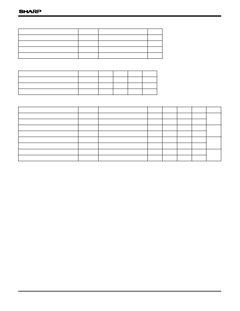
ABSOLUTE MAXIMUM RATINGS
RECOMMENDED OPERATING CONDITIONS
PARAMETER
SYMBOL
Power supply voltage
V
DD
Input voltage
V
I
Output voltage
V
O
ELECTRICAL CHARACTERISTICS
(V
DD
= 3.0±0.3 V, T
OPR
= ≠20 to +70 ∞C)
Storage temperature
T
STG
≠55 to +150
≠0.3 to V
DD
+ 0.3
≠0.3 to V
DD
+ 0.3
≠0.3 to +4.3
RATING
UNIT
V
V
V
∞C
PARAMETER
SYMBOL
Power supply voltage
V
DD
Operating temperature
T
OPR
Input clock frequency
f
CK
≠20
2.7
MIN.
UNIT
V
∞C
MHz
TYP.
MAX.
3.0
3.3
+25
+70
9.0
Input "Low" voltage
V
IL
Input "High" voltage
V
IH
Input "Low" current
|I
IL1
|
|I
IH1
|
Input "Low" current
|I
IL2
|
Input "High" current
|I
IH2
|
Output "High" voltage
V
OH
PARAMETER
SYMBOL
CONDITIONS
Input "High" current
V
OL
Output "Low" voltage
MIN.
0.8V
DD
0.8V
DD
40
100
TYP.
MAX.
1.0
1.0
0.2V
DD
0.2V
DD
2.0
300
V
I
= 0 V
V
IN
= V
DD
V
IN
= 0 V
I
OH
= ≠4 mA
I
OL
= 4 mA
V
IN
= V
DD
µA
µA
V
V
V
V
µA
µA
UNIT
NOTE
2
1
4
3
NOTES :
1. Applied to input (IC) and inputs/outputs (IO4M, IO4MU).
2. Applied to input (IC) and input/output (IO4M).
3. Applied to input/output (IO4MU).
4. Applied to output (OBF4M) and inputs/outputs (IO4M, IO4MU).

LR38630
19
(APPENDIX)
Weighting area of exposure control
1 block = 44 pixels in horizontal and 36 lines in vertical
q (Bit 3, Bit 2) of address 0Ch = (0, 0)
w (Bit 3, Bit 2) of address 0Ch = (0, 1)
e (Bit 3, Bit 2) of address 0Ch = (1, 0)
r (Bit 3, Bit 2) of address 0Ch = (1, 1)
2/4
2/4
2/4
2/4
2/4
2/4
2/4
2/4
2/4
2/4
2/4
2/4
2/4
2/4
2/4
2/4
1
1
1
1
1
1
1
1
1
1
1
1
1
1
1
1
1
1
1
1
1
1
1
1
1
1
1
5/4
5/4
5/4
5/4
1
1
5/4
5/4
5/4
5/4
1
1
1
1
5/4
5/4
5/4
5/4
1
1
1
1
5/4
5/4
5/4
5/4
1
1
1
3/4
3/4
3/4
3/4
3/4
3/4
3/4
3/4
3/4
3/4
5/4
5/4
5/4
5/4
5/4
5/4
5/4
5/4
5/4
5/4
5/4
5/4
3/4
3/4
3/4
3/4
5/4
5/4
5/4
5/4
5/4
5/4
3/4
3/4
5/4
5/4
5/4
5/4
5/4
5/4
5/4
5/4
5/4
5/4
5/4
5/4
3/4
3/4
1
5/4
5/4
5/4
5/4
5/4
5/4
3/4
3/4
1
1
1
1
1
1
1
1
1
1
1
1
1
1
1
1
1
1
1
1
1
1
1
1
1
1
1
1
1
1
1
1
1
1
1
1
1
1
1
1
1
1
1
1
1
1
1
1
1
1
1
1
1
1
1
1
1
1
1
1
1
1
1
1
1
1
1
1
1
1
1
2/4
2/4
2/4
2/4
2/4
2/4
2/4
2/4
2/4
2/4
2/4
2/4
2/4
2/4
2/4
2/4
1
1
1
1
1
1
1
1
5/4
5/4
5/4
5/4
5/4
5/4
5/4
5/4
5/4
5/4
5/4
5/4
5/4
5/4
5/4
5/4
5/4
5/4
5/4
5/4
5/4
5/4
5/4
5/4
5/4
5/4
5/4
5/4
5/4
5/4
5/4
5/4

PACKAGES FOR CCD AND CMOS DEVICES
20
PACKAGE
(Unit : mm)
1
0.1
±0.1
Package
base plane
60
0.5
TYP.
0.2
±0.08
41
40
(1.0)
12.0
±0.2
21
(1.0)
20
(1.0)
(1.0)
12.0
±0.2
14.0
±0.3
61
80
13.0
±0.2
M
0.08
0.10
0.125
±0.05
0.6375
1.40
±0.2
14.0
±0.3
1.70
MAX.
80 LQFP (LQFP080-P-1212)