PC852X/PC853X
PC852X/PC853X
1. Telephones
2. Facsimiles
3. Modems
4. Set-top Boxes
Features
Applications
High Collector-emitter Voltage
Type Photocouplers
1. High collector-emitter voltage
(V
CEO
:350V)
2. High current transfer ratio
(CTR:MIN. 1 000% at I
F
=1mA, V
CE
=2V)
3. High isolation voltage between input and output
(V
iso (rms)
:5kV)
4. Compact dual-in-line package
5. Large collector power dissipation
PC853X (P
C
:300mW)
6. Recognized by UL, file NO. E64380
(model No. PC852/PC853)
Notice
In the absence of confirmation by device specification sheets, SHARP takes no responsibility for any defects that may occur in equipment using any SHARP
devices shown in catalogs, data books, etc. Contact SHARP in order to obtain the latest device specification sheets before using any SHARP device.
Internet
Internet address for Electronic Components Group http://sharp-world.com/ecg/
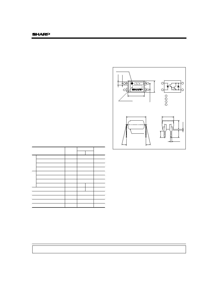
Outline Dimensions
(Unit : mm)
4.58
�
0.5
0.6
�
0.2
1.2
�
0.3
2.54
�
0.25
6.5
�0.5
Model No.
7.62
�0.3
4.58
�0.5
3.5
�
0.5
3.0
�
0.5
2.7
�
0.5
0.5
TYP.
Anode mark
0.5
�0.1
: 0 to 13�
Epoxy resin
1
2
4
3
Internal connection
diagram
1
2
3
4
Anode
Anode
Cathode
Emitter
Collector
1
2
4
3
Absolute Maximum Ratings
(T
a
=25�C)
Parameter
Symbol
Unit
Input
Forward current
mA
*1
Peak forward current
A
Power dissipation
mW
Output
Collector-emitter voltage
V
Emitter-collector voltage
V
Collector current
mA
Collector power dissipation
mW
Total power dissipation
mW
*2
Isolation voltage
Operating temperature
�C
Storage temperature
�C
*3
Soldering temperature
I
F
I
FM
P
V
CEO
V
ECO
I
C
P
C
P
tot
V
iso (rms)
T
opr
T
stg
T
sol
�C
*1 Pulse width
100�s, Duty ratio:0.001
*2 40 to 60%RH, AC for 1 minute
*3 For 10s
Rating
PC852X PC853X
50
1
Reverse voltage
V
V
R
6
70
350
0.1
150
150
200
300
320
-30 to +100
-55 to +125
260
5
kV
Lead forming type (I type) and taping reel type (P type) are also available. (PC852XI/PC852XP/PC853XI/PC853XP)
PC852X/PC853X
Electro-optical Characteristics
Parameter
Conditions
Forward voltage
Reverse current
Terminal capacitance
Collector dark current
Transfer
charac-
teristics
Collector current
Collector-emitter saturation voltage
Isolation resistance
Floating capacitance
Cut-off frequency
MIN.
-
-
-
-
10
-
5
�10
10
-
1
-
-
TYP.
1.2
-
30
-
40
-
10
11
0.6
7
100
20
MAX.
1.4
10
250
200
150
1.2
-
1.0
-
300
100
Unit
V
�A
pF
nA
mA
V
pF
kHz
�s
�s
Symbol
V
F
I
R
C
t
I
CEO
I
C
V
CE (sat)
R
ISO
f
c
t
r
t
f
C
f
Response time
Rise time
Fall time
Input
Output
I
F
=10mA
V
R
=4V
V
=0, f=1kHz
V
CE
=200V, I
F
=0
I
F
=1mA, V
CE
=2V
I
F
=20mA, I
C
=100mA
V
=0, f=1MHz
V
CE
=2V, I
C
=20mA, R
L
=100
V
CE
=2V, I
C
=20mA, R
L
=100, -3dB
DC500V, 40 to 60%RH
(T
a
=25�C)
Collector-emitter breakdown voltage
350
-
-
V
BV
CEO
I
C
=0.1mA, I
F
=0
0
0
125
100
200
50
150
25
50
75
100
-30
Collector power dissipation P
C
(mW)
Ambient temperature T
a
(�C)
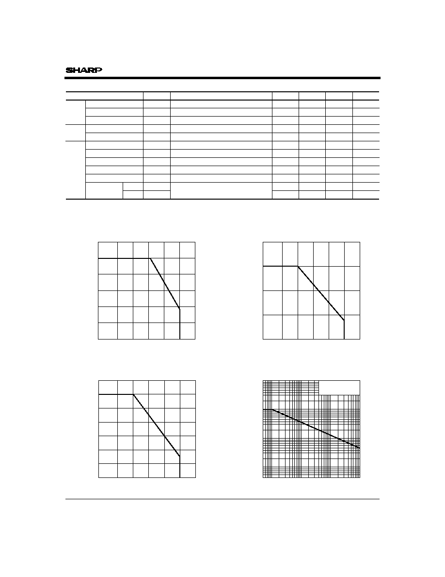
Fig.2-a Collector Power Dissipation vs.
Ambient Temperature
(PC852X)
0
-30
10
0
25
50
75
100
125
20
30
40
50
60
Ambient temperature T
a
(�C)
Forward current I
F
(mA)
Fig.1 Forward Current vs. Ambient
Temperature
Duty ratio
5
5
Pulse width
100�s
T
a
=25�C
10
20
100
50
200
500
2
10
-3
10
-2
5
2
10
-1
5
2
5
Peak forward current I
FM
(mA)
1
10 000
5 000
2 000
1 000
Fig.3 Peak Forward Current vs. Duty Ratio
0
100
350
50
150
250
200
300
Collector power dissipation P
C
(mW)
Ambient temperature T
a
(�C)
-30
0
25
50
75
100
125
Fig.2-b Collector Power Dissipation vs.
Ambient Temperature
(PC853X)
PC852X/PC853X
0
0.1
Current transfer ratio CTR (%)
0.2
0.5
10
1
2
5
Forward current I
F
(mA)
V
CE
=2V
T
a
=25�C
5 000
4 000
3 000
2 000
1 000
Fig.5-a Current Transfer Ratio vs. Forward
Current
50
0
100
150
0
20
40
60
80
100
Relative current transfer ratio (%)
Ambient Temperature T
a
(�C)
I
F
=1mA
V
CE
=2V
-30
Fig.7 Relative Current Transfer Ratio vs.
Ambient Temperature
0
0
100
200
1
2
3
4
5
0.5mA
1mA
1.5mA
2mA
2.5mA
3mA
5mA
Collector current I
C
(mA)
Collector-emitter voltage V
CE
(V)
P
C
(MAX.)
T
a
=25�C
I
F
=10mA
Fig.6-a Collector Current vs. Collector-
emitter Voltage
0
0.1
Current transfer ratio CTR (%)
0.2
0.5
10
1
2
5
Forward current I
F
(mA)
V
CE
=2V
T
a
=25�C
5 000
4 000
3 000
2 000
1 000
Fig.5-b Current Transfer Ratio vs. Forward
Current
0.5mA
1mA
1.5mA
2mA
2.5mA
3mA
5mA
P
C
(MAX.)
I
F
=10mA
0
0
100
200
1
2
3
4
5
Collector current I
C
(mA)
Collector-emitter voltage V
CE
(V)
T
a
=25�C
Fig.6-b Collector Current vs. Collector-
emitter Voltage
0
2
0.5
1.0
1.5
2.0
2.5
3.0
3.5
5
10
20
50
100
200
500
1
Forward voltage V
F
(V)
Forward current I
F
(mA)
50�C
25�C
0�C
-25�C
T
a
=75�C
Fig.4 Forward Current vs. Forward Voltage
(PC852X)
(PC853X)
(PC852X)
(PC853X)
PC852X/PC853X
Frequency f (kHz)
0
0.1
1
10
100
100
10
Voltage gain A
v
(dB)
V
CE
=2V
I
C
=20mA
T
a
=25�C
R
L
=1k
1 000
-25
-20
-15
-10
-5
Fig.11 Frequency Response
Collector-emitter saturation voltage V
CE (sat)
(V)
Forward current I
F
(mA)
0
0
1
2
3
4
5
1
2
3
4
5
10mA
30mA
50mA
70mA
100mA
T
a
=25�C
I
C
=5mA
Fig.12 Collector-emitter Saturation Voltage
vs. Forward Current
0
-30
0.2
0
20
40
60
80
100
0.4
0.6
0.8
1.0
1.2
Ambient temperature T
a
(�C)
Collector-emitter saturation voltage V
CE (sat)
(V)
I
F
=20mA
I
C
=100mA
Fig.8 Collector-emitter Saturation Voltage
vs. Ambient Temperature
20
0
40
60
80
100
10
-10
10
-9
10
-8
10
-7
10
-6
10
-5
Collector dark current I
CEO
(A)
Ambient temperature T
a
(�C)
V
CE
=200V
-30
10
-11
Fig.9 Collector Dark Current vs. Ambient
Temperature
Response time (
�
s)
2
1
5
10
20
50
100
200
500
0.01
0.1
1
10
V
CE
=2V
I
C
=20mA
T
a
=25�C
t
r
t
f
t
d
t
s
1 000
Load resistance R
L
(k
)
Fig.10 Response Time vs. Load Resistance

SPECIFICATIONS ARE SUBJECT TO CHANGE WITHOUT NOTICE.
Suggested applications (if any) are for standard use; See Important Restrictions for limitations on special applications. See Limited
Warranty for SHARP's product warranty. The Limited Warranty is in lieu, and exclusive of, all other warranties, express or implied.
ALL EXPRESS AND IMPLIED WARRANTIES, INCLUDING THE WARRANTIES OF MERCHANTABILITY, FITNESS FOR USE AND
FITNESS FOR A PARTICULAR PURPOSE, ARE SPECIFICALLY EXCLUDED. In no event will SHARP be liable, or in any way responsible,
for any incidental or consequential economic or property damage.
NORTH AMERICA
EUROPE
JAPAN
SHARP Microelectronics of the Americas
5700 NW Pacific Rim Blvd.
Camas, WA 98607, U.S.A.
Phone: (1) 360-834-2500
Fax: (1) 360-834-8903
Fast Info: (1) 800-833-9437
www.sharpsma.com
SHARP Microelectronics Europe
Division of Sharp Electronics (Europe) GmbH
Sonninstrasse 3
20097 Hamburg, Germany
Phone: (49) 40-2376-2286
Fax: (49) 40-2376-2232
www.sharpsme.com
SHARP Corporation
Electronic Components & Devices
22-22 Nagaike-cho, Abeno-Ku
Osaka 545-8522, Japan
Phone: (81) 6-6621-1221
Fax: (81) 6117-725300/6117-725301
www.sharp-world.com
TAIWAN
SINGAPORE
KOREA
SHARP Electronic Components
(Taiwan) Corporation
8F-A, No. 16, Sec. 4, Nanking E. Rd.
Taipei, Taiwan, Republic of China
Phone: (886) 2-2577-7341
Fax: (886) 2-2577-7326/2-2577-7328
SHARP Electronics (Singapore) PTE., Ltd.
438A, Alexandra Road, #05-01/02
Alexandra Technopark,
Singapore 119967
Phone: (65) 271-3566
Fax: (65) 271-3855
SHARP Electronic Components
(Korea) Corporation
RM 501 Geosung B/D, 541
Dohwa-dong, Mapo-ku
Seoul 121-701, Korea
Phone: (82) 2-711-5813 ~ 8
Fax: (82) 2-711-5819
CHINA
HONG KONG
SHARP Microelectronics of China
(Shanghai) Co., Ltd.
28 Xin Jin Qiao Road King Tower 16F
Pudong Shanghai, 201206 P.R. China
Phone: (86) 21-5854-7710/21-5834-6056
Fax: (86) 21-5854-4340/21-5834-6057
Head Office:
No. 360, Bashen Road,
Xin Development Bldg. 22
Waigaoqiao Free Trade Zone Shanghai
200131 P.R. China
Email: smc@china.global.sharp.co.jp
SHARP-ROXY (Hong Kong) Ltd.
3rd Business Division,
17/F, Admiralty Centre, Tower 1
18 Harcourt Road, Hong Kong
Phone: (852) 28229311
Fax: (852) 28660779
www.sharp.com.hk
Shenzhen Representative Office:
Room 13B1, Tower C,
Electronics Science & Technology Building
Shen Nan Zhong Road
Shenzhen, P.R. China
Phone: (86) 755-3273731
Fax: (86) 755-3273735