 | –≠–ª–µ–∫—Ç—Ä–æ–Ω–Ω—ã–π –∫–æ–º–ø–æ–Ω–µ–Ω—Ç: PQ05RR1B | –°–∫–∞—á–∞—Ç—å:  PDF PDF  ZIP ZIP |
" In the absence of confirmation by device specification sheets,SHARP takes no responsibility for any defects that may occur in equipment using any SHARP devices
shown in catalogs,data books,etc.Contact SHARP in order to obtain the latest version of the device specification sheets before using any SHARP's device. "
Low Power-Loss Voltage Regulators
PQ05RR1/PQ05RR11/PQ05RR1B
s
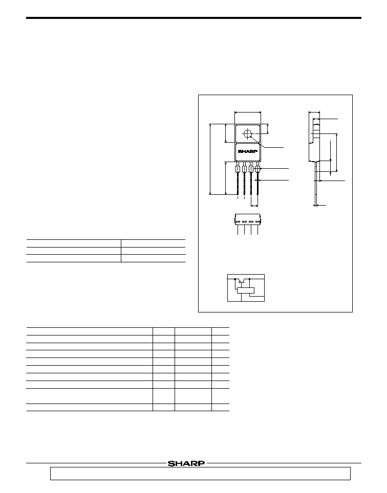
Outline Dimensions
(Unit : mm)
s
Features
°Low power-loss (Dropout voltage : MAX. 0.5V)
°Compact resin full-mold package
°Built-in reset signal generating function to prevent errors of
microcomputer when the output voltage drops.
°Lead forming type
(PQ05RR1B
) is also available.
PQ05RR1/11/1B
1A Output, Low Power-Loss Voltage Regulators(Built-in Reset Signal Generating Function)
PQ05RR1
PQ05RR11
Output voltage precision:±5%
Output voltage precision:±2.5%
s
Model Line-ups
5V output
Output voltage
s
Applications
° Series power supply for equipment provided with
microcomputer such as electronic musical instruments and
VCRs
Parameter
Symbol
Rating
Unit
V
IN
V
r
I
O
I
r
P
D1
P
D2
T
j
T
opr
T
stg
T
sol
35
35
1
10
1.5
15
150
-20 to +80
-40 to +150
260 (For 10s)
V
V
A
mA
W
W
∞C
∞C
∞C
∞C
Input voltage
Reset output voltage
Output current
Reset output current
Power dissipation(No heat sink)
Power dissipation(With infinite heat sink)
Junction temperature
Operating temperature
Storage temperature
Soldering temperature
*1
*1
*2
*1
All are open except GND and applicable terminals.
*2
Overheat protection may operate at 125=<T
j
=<150∞C
s
Absolute Maximum Ratings
(T
a
=25∞C)
2
3
1
4
PQ05RR1
Internal connection diagram
Specific IC
29.1MAX
10.2MAX
7.4±0.2
3.6±0.2
3.2±0.1
+0.3
-0
4-1.4
+0.2
-0.1
4-0.6
13.5MIN
3-(2.54)
4.5±0.2
2.8±0.2
15.6±0.5
4.8MAX
(1.5)
(0.5)
q
1
q
2
q
3
q
4
1 DC input (V
IN
)
2 DC output (V
O
)
3 GND
4 Reset signal output (V
r
)
∑ Please refer to the chapter" Handling Precautions ".
Low Power-Loss Voltage Regulators
PQ05RR1/PQ05RR11/PQ05RR1B
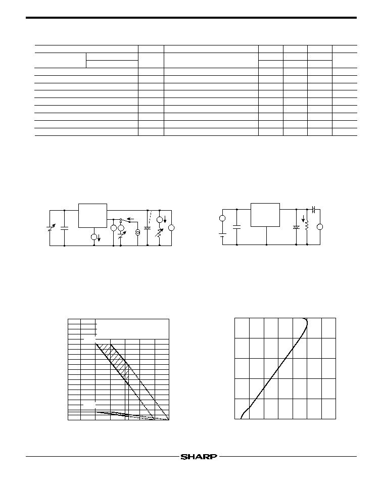
Fig.1 Test Circuit
Fig.2 Test Circuit of Ripple Rejection
Fig.3 Power Dissipation vs. Ambient
Temperature
Fig.4 Overcurrent Protection
Characteristics (Typical Value)
Parameter
Symbol
Conditions
V
O
R
eg
L
R
eg
I
T
C
V
O
RR
V
i
-o
V
rl
V
rt
I
rlk
I
q
Output voltage
Load regulation
Line regulation
Temperature coefficient of output voltage
Ripple rejection
Dropout voltage
Low reset output voltage
Reset threshold voltage
Reset output leak current
Quiescent current
Unit
MAX.
TYP.
MIN.
PQ05RR1
PQ05RR11
4.75
4.88
-
-
-
45
-
-
V
O
-0.25
-
-
-
I
O
=5mA
to
1.0A
V
IN
=6 to 12V
T
j
=0 to 125∞C
Refer to Fig. 2
*3
I
O
=5mA, I
r
=5mA
I
O
=5mA
I
O
=5mA, V
r
=35V
I
O
=0
5.0
5.0
0.1
0.5
±0.02
55
-
-
-
-
-
5.25
5.12
2.0
2.5
-
-
0.5
0.8
V
O
-0.1
30
10
s
Electrical Characteristics
*3
Input voltage shall be the value when output voltage is 95% in comparison with the initial value.
(Unless otherwise specified, condition shall be V
IN
=7V, Io=0.5A, T
a
=25∞C)
V
%
%
%/∞C
dB
V
V
V
µ
A
mA
q
3
q
2
q
1
q
4
A
V
A
A
V
V
IN
I
q
I
O
V
O
V
r
R
L
0.33
µ
F
47
µ
F
I
rlk
+
I
O
V
rl
P
D1
:No heat sink
P
D2
:With infinite heat sink
Power dissipation P
D
(W)
Ambient temperature T
a
(∞C)
0
-20
0
P
D1
P
D2
50
100
150
5
10
15
20
Note)
Oblique line portion:Overheat protection may
operate in this area.
q
3
q
2
q
1
q
4
V
e
i
V
IN
I
O
e
o
R
L
0.33
µ
F
47
µ
F
+
+
~
~
f=120Hz (sine wave)
e
i
=0.5V
rms
RR=20 log (e
i
/e
o
)
0
0.6
0.3
1.5
1.2
0.9
1.8
2.1
100
80
40
60
20
0
Relative output voltage (%)
Output current I
O
(A)
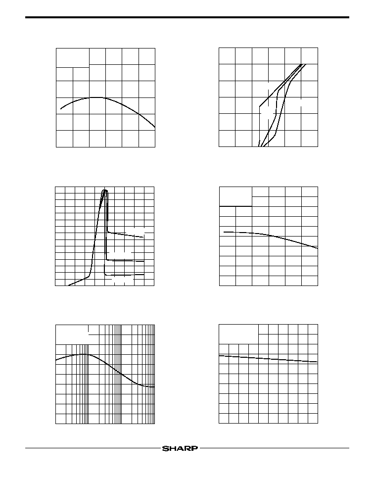
Low Power-Loss Voltage Regulators
PQ05RR1/PQ05RR11/PQ05RR1B
Fig.5 Output Voltage Deviation vs. Junction
Temperature
Fig.7 Circuit Operating Current vs. Input
Voltage (Typical Value)
Fig.9 Ripple Rejection vs. Input Ripple
Frequency
Fig.8 Quiescent Current vs. Junction
Temperature
Fig.10 Ripple Rejection vs. Output Current
Fig.6 Output Voltage vs. Input Voltage
(Typical Value)
-30
-20
0
25
50
75
100
125
0
V
IN
=7V
I
O
=0.5A
+30
Output voltage deviation
V
O
(mV)
Junction temperature T
j
(∞C)
0
0
1
3
2
5
4
6
6
5
4
3
2
1
Output voltage V
O
(V)
Input voltage V
IN
(V)
R
L
=
R
L
=
10
R
L
=5
0
0
5
10
10
20
30
R
L
=
R
L
=5
R
L
=10
Circuit operating current I
BIAS
(mA)
Input voltage V
IN
(V)
0
-25
0
25
50
75
100
125
5
V
IN
=35V
I
O
=0A
10
Quiescent current I
q
(mA)
Junction temperature T
j
(∞C)
0
0.1
10
1
100
20
40
60
80
100
Input ripple frequency f
(kHz)
e
i
=
0.5
V
rms
I
O
=0.5A
V
IN
=7V
Ripple rejection RR (dB)
0
0
0.5
1.0
80
60
40
20
100
Ripple rejection RR (dB)
Output current I
O
(A)
f
=
120Hz
e
i
=
0.5
V
rms
V
IN
=
7V
Low Power-Loss Voltage Regulators
PQ05RR1/PQ05RR11/PQ05RR1B
Fig.11 Output Peak Current vs. Junction
Temperature
Fig.12 Output Peak Current vs. Dropout
Voltage
Fig.13 Reset Output Delay Time vs. Time
Constant
-25
0
50
25
100
75
125
1.9
1.5
I
OP
:Output current when
output voltage is 95% in
comparison with the initial value
1.0
Output peak current I
OP
(A)
Junction temperature T
j
(∞C)
V
IN-
V
O
=5V
2V
1V
0.5V
1.0
0
1
2
3
4
5
6
1.5
2.0
Output peak current I
OP
(A)
Dropout voltage V
i
-O
(V)
0
0.8V
R
r
=10k
V
r
t
T
r
Reset cancel
q
2
q
3
q
1
q
4
V
O
C
O
R
r
V
r
C
r
V
IN
Load
+
0.01
0.1
1.0
10.0
10
-4
10
-2
10
-3
10
-1
Reset output voltage delay time T
r
(ms)
Time constant
(C
r
XR
r
)
R
r
=10k
Low Power-Loss Voltage Regulators
PQ05RR1/PQ05RR11/PQ05RR1B
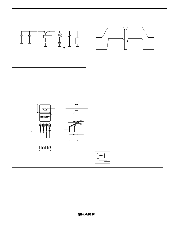
s
Typical Application
s
Reset Output Response Characteristics
Note) The value of absolute maximum ratings and electrical characteristics is same as ones of
PQ05RR11
.
s
Outline Dimensions
(Unit : mm)
PQ05RR1
2
3
1
4
Specific IC
Internal connection diagram
∑ ( ) : Typical value
∑ Radius of lead forming portion : R=0.5 to 1.5mm
(24.6)
10.2MAX
7.4±0.2
3.6±0.2
3.2±0.1
+0.3
-0
4-1.4
+0.2
-0.1
4-0.6
3-(2.54)
4.5±0.2
2.8±0.2
16.4±0.7
(2.0)
(3.2)
q
1
q
2
q
3
q
4
5±0.5
5±0.5
8.2±0.7
(0.5)
(1.5)
4.4MIN
1 DC input (V
IN
)
2 DC output (V
O
)
3 GND
4 Reset signal output (V
r
)
Specific IC
q
2
q
3
q
1
q
4
R
L
V
O
C
O
R
r
C
r
Reset output
*Open collector output
*
V
IN
DC input
+
+
PQ05RR1B
Output voltage precision:±2.5%
s
Model Line-up for Lead Forming Type
5Voutput
Output voltage
V
O
V
r