 | –≠–ª–µ–∫—Ç—Ä–æ–Ω–Ω—ã–π –∫–æ–º–ø–æ–Ω–µ–Ω—Ç: PQ05TZ51 | –°–∫–∞—á–∞—Ç—å:  PDF PDF  ZIP ZIP |
" In the absence of confirmation by device specification sheets,SHARP takes no responsibility for any defects that may occur in equipment using any SHARP devices
shown in catalogs,data books,etc.Contact SHARP in order to obtain the latest version of the device specification sheets before using any SHARP's device. "
Low Power-Loss Voltage Regulators
PQ05TZ51/PQ05TZ11 Series
PQ05TZ51/PQ05TZ11 Series
Low Power-Loss Voltage Regulators with OFF-state Low Dissipation Current
s
Features
s
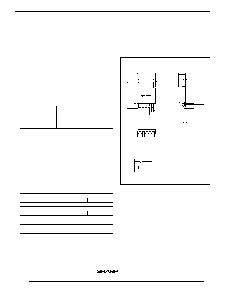
Outline Dimensions
(Unit : mm)
Output voltage
PQ05TZ51
PQ05TZ11
Output voltage
precision:±2.5%
Output voltage
precision:±2.5%
s
Model Line-ups
5V Output
0.5A
Output
1.0A
Output
PQ09TZ51
PQ09TZ11
9V Output
PQ12TZ51
PQ12TZ11
12V Output
Parameter
Symbol
Rating
Unit
V
IN
V
C
I
O
P
D
T
j
T
opr
T
stg
T
sol
PQ
XX
TZ51
0.5
V
V
A
W
∞C
∞C
∞C
∞C
Input voltage
Output control voltage
Output current
Power dissipation
Junction temperature
Operating temperature
Storage temperature
Soldering temperature
*1
*1
*2
*3
*1
All are open except GND and applicable terminals.
*2
With infinite heat sink.
*3
Overheat protection may operate at 125∞C=<T
j
=<150∞C
s
Absolute Maximum Ratings
(
XX
=05,09,12, T
a
=25∞C)
PQ
XX
TZ11
1.0
24
24
8
150
-20 to +80
-40 to +150
260 (For 10s)
05TZ51
6.6MAX
9.7MAX
2.5MIN
5.2±0.5
2.3±0.5
5.5±0.5
(0.5)
(0.5)
(0.9)
(1.7)
3
0.5
+0.2
-0.1
4-(1.27)
1
3
2
4 5
3
5
1
2
Specific IC
(0to0.25)
1 DC input (V
IN
)
2 ON/OFF control
terminal (V
C
)
3 DC output (V
O
)
4 NC
5 GND
Heat sink is common to 3 (V
O
).
Internal connection diagram
∑ Please refer to the chapter" Handling Precautions ".
°Low power-loss (Dropout voltage : MAX 0.5V)
°Surface mount type package (Equivalent to EIAJ SC-63)
°Both the 0.5A output
PQ05TZ51 series
and the 1A output
PQ05TZ11 series
have high-precision output (±2.5%)
°Low dissipation current at OFF-state (Iqs:MAX.5µA)
°Built-in ON/OFF control function
Low Power-Loss Voltage Regulators
PQ05TZ51/PQ05TZ11 Series
Parameter
Symbol
Conditions
V
O
R
eg
L
R
eg
I
T
C
V
O
RR
V
i
-
O
V
C
(
ON
)
I
C
(
ON
)
V
C
(
OFF
)
I
C
(
OFF
)
I
q
I
qs
Load regulation
Line regulation
Temperature coefficient of output voltage
Ripple rejection
Dropout voltage
ON-state voltage for control
ON-state current for control
OFF-state voltage for control
OFF-state current for control
Quiescent current
Output OFF-state dissipation current
Unit
MAX.
TYP.
MIN.
PQ05TZ51/11
PQ09TZ51/11
PQ12TZ51/11
4.88
8.78
11.7
-
-
-
45
-
2.0
-
-
-
-
-
*3,*7
*3,*4
Io=5mA,
*8
*3
,Io=5mA, T
j
=0 to 125∞C
Refer to Fig. 2
*7,*5
*3,*6,*7
*3,*7
*3
*3
,V
C
=0.4V
*3
,I
O
=0A
*3
,V
C
=0.4V,I
O
=0A
5.0
9.0
12.0
0.2
0.1
±0.01
60
0.2
-
-
-
-
4
-
5.12
9.22
12.3
2.0
2.5
-
-
0.5
-
200
0.8
10
10
5
Output voltage
s
Electrical Characteristics
*3
PQ05TZ51/11
:V
IN
= 7V
PQ09TZ51/11
:V
IN
=11V
PQ12TZ51/11
:V
IN
=14V
*4
PQxxTZ51
:Io=5mA to 0.5A,
PQxxTZ51
:Io=5mA to 1.0A
*5
Input voltage shall be the value when output voltage is 95% in comparison with the initial value.
*6
In case of opening control terinal 2, output voltage turns off.
*7
PQxxTZ51
:Io=0.3A,
PQxxTZ11
:Io=0.5A
*8
PQ05TZ51/11
:V
IN
=6V to 16V
PQ09TZ51/11
:V
IN
=10V to 20V
PQ12TZ51/11
:V
IN
=13V to 23V
(Unless otherwise specified,Vc=2.7V,T
a
=25∞C)
V
%
%
%/∞C
dB
V
V
µ
A
V
µ
A
mA
µ
A
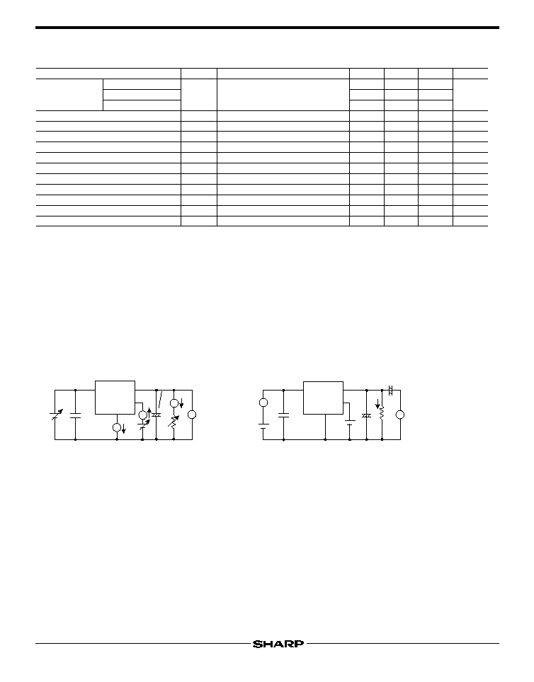
Fig.1
Test Circuit
Fig.2
Test Circuit of Ripple Rejection
q
5
q
3
q
1
q
2
A
V
A
A
V
IN
I
q
I
C
I
O
V
O
V
C
R
L
0.33
µ
F
47
µ
F
+
q
5
q
3
q
1
q
2
V
e
i
V
IN
2.7V
I
O
e
o
R
L
0.33
µ
F
47
µ
F
+
+
~
~
V
C
f=120Hz (sine wave)
e
i
=0.5V
rms
V
IN
= 7V (
PQ05TZ51/11
)
V
IN
=11V (
PQ09TZ51/11
)
V
IN
=14V (
PQ12TZ51/11
)
I
O
=0.3A
RR=20 log (e
i
/e
o
)
Low Power-Loss Voltage Regulators
PQ05TZ51/PQ05TZ11 Series
Relative output voltage (%)
Output current I
O
(A)
0
0
20
40
60
80
100
0.3
0.6
0.9
1.2
1.5
1.8
2.1
PQxxTZ5/51
PQxxTZ1/11
Output voltage deviation
V
O
(mV)
Junction temperature T
j
(∞C)
-25
0
0
-50
-45
-40
-35
-30
-25
-20
-15
-10
- 5
5
10
15
20
25
30
35
25
50
75
100
125
V
IN
=7V , I
O
=5mA , V
C
=2.7V
-25
0
0
-90
-80
-70
-60
-50
-40
-30
-20
-10
10
20
30
40
50
60
70
25
50
75
100
125
V
IN
=11V , I
O
=5mA , V
C
=2.7V
Output voltage deviation
V
O
(mV)
Junction temperature T
j
(∞C)
Output voltage deviation
V
O
(mV)
Junction temperature T
j
(∞C)
-
25
0
0
-90
-80
-70
-60
-50
-40
-30
-20
-10
10
20
30
40
50
60
70
25
50
75
100
125
V
IN
=14V , I
O
=5mA , V
C
=2.7V
Output voltage V
O
(V)
Input voltage V
IN
(V)
0
1
2
3
4
5
6
7
8
1
2
3
4
5
6
7
V
C
=2.7V , C
i
=0.33
µ
F , C
0
=47
µ
F
R
L
=20
R
L
=10
R
L
=
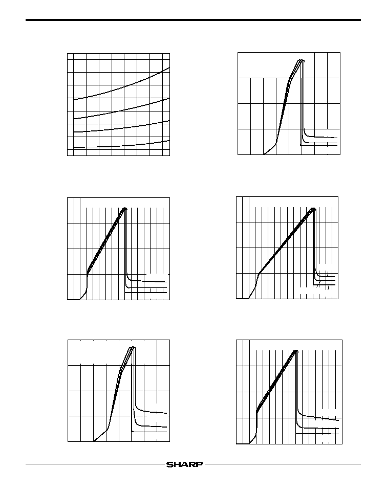
Fig.3 Power Dissipation vs. Ambient
Temperature
Fig.5 Output Voltage Deviation vs. Junction
Temperature (PQ05TZ51/11)
Fig.7 Output Voltage Deviation vs. Junction
Temperature (PQ12TZ51/11)
Fig.6 Output Voltage Deviation vs. Junction
Temperature (PQ09TZ51/11)
Fig.8 Output Voltage vs. Input Voltage
(PQ05TZ51)
Fig.4 Overcurrent Protection Characteristics
(Typical Value) (xx=05,09,12)
,,
,,
,,
-20
0
0
5
10
20
40
60
80
100
P
D
With infinite heat sink
Power dissipation P
D
(W)
Ambient temperature T
a
(∞C)
Note) Oblique line portion : Overheat protection may
operate in this area.
Low Power-Loss Voltage Regulators
PQ05TZ51/PQ05TZ11 Series
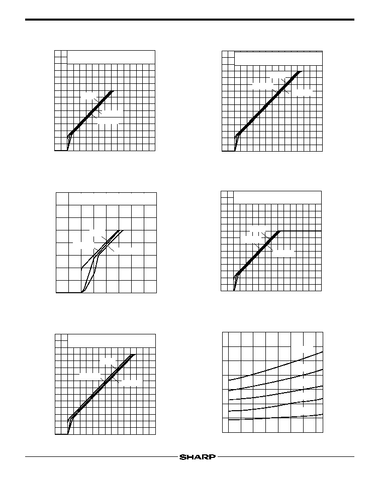
Output voltage V
O
(V)
Input voltage V
IN
(V)
0
5
15
10
5
15
V
C
=2.7V , C
i
=0.33
µ
F , C
0
=47
µ
F
T
j
=25∞C
R
L
=36
R
L
=18
R
L
=
10
Output voltage V
O
(V)
Input voltage V
IN
(V)
10
0
5
15
10
5
15
V
C
=2.7V , C
i
=0.33
µ
F , C
0
=47
µ
F
T
j
=25∞C
R
L
=24
R
L
=48
R
L
=
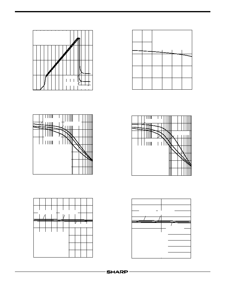
Fig.9 Output Voltage vs. Input Voltage
(Typical Value) (PQ09TZ51)
Fig.11 Output Voltage vs. Input Voltage
(Typical Value) (PQ05TZ11)
Fig.13 Output Voltage vs. Input Voltage
(PQ12TZ11)
Fig.12 Output Voltage vs. Input Voltage
(PQ09TZ11)
Fig.14 Dropout Voltage vs. Junction Temperature
(PQ05TZ51/PQ09TZ51/PQ12TZ51)
Fig.10 Output Voltage vs. Input Voltage
(Typical Value) (PQ12TZ51)
Output voltage V
O
(V)
Input voltage V
IN
(V)
0
1
2
3
4
5
6
7
8
1
2
3
4
5
6
7
8
V
C
=2.7V , C
i
=0.33
µ
F , C
0
=47
µ
F
T
j
=25∞C
R
L
=5
R
L
=10
R
L
=
Output voltage V
O
(V)
Input voltage V
IN
(V)
10
0
5
15
10
5
15
V
C
=2.7V , C
i
=0.33
µ
F , C
0
=47
µ
F
T
j
=25∞C
R
L
=12
R
L
=24
R
L
=
Junction temperature T
j
(∞C)
Dropout voltage V
i
-O
(V)
-20
0
20
40
60
80 100 120
0
0.05
0.10
0.15
0.20
0.25
0.30
I
O
=0.5A
I
O
=0.4A
I
O
=0.3A
I
O
=0.2A
I
O
=0.1A
Output voltage V
O
(V)
Input voltage V
IN
(V)
10
0
5
15
10
5
15
V
C
=2.7V , C
i
=0.33
µ
F , C
0
=47
µ
F
T
j
=25∞C
R
L
=9
R
L
=18
R
L
=
Low Power-Loss Voltage Regulators
PQ05TZ51/PQ05TZ11 Series
Fig.15 Dropout Voltage vs. Junction Temperature
(PQ05TZ11/PQ09TZ11/PQ12TZ11)
Fig.17 Circuit Operating Current vs. Input
Voltage (PQ09TZ51)
Fig.19 Circuit Operating Current vs. Input
Voltage (PQ05TZ11)
Fig.18 Circuit Operating Current vs. Input
Voltage (PQ12TZ51)
Fig.20 Circuit Operating Current vs. Input
Voltage (PQ09TZ11)
Fig.16 Circuit Operating Current vs. Input
Voltage (PQ05TZ51)
Junction temperature T
j
(∞C)
Dropout voltage V
i
-O
(V)
-20
0
20
40
60
80 100 120
0.05
0.10
0.15
0.20
0.25
0.30
0.35
0.40
I
O
=1.0A
I
O
=0.75A
I
O
=0.5A
I
O
=0.25A
Input voltage V
IN
(V)
Circuit operating current I
BIAS
(mA)
0
1
2
3
4
5
6
7
8
10
20
30
V
C
=2.7V
, C
i
=0.33
µ
F
C
0
=47
µ
F
R
L
=20
R
L
=10
R
L
=
Input voltage V
IN
(V)
Circuit operating current I
BIAS
(mA)
0
5
10
15
10
20
30
V
C
=2.7V
, C
i
=0.33
µ
F
, C
0
=47
µ
F
R
L
=36
R
L
=18
R
L
=
Input voltage V
IN
(V)
Circuit operating current I
BIAS
(mA)
0
5
10
15
10
20
30
V
C
=2.7V
, C
i
=0.33
µ
F
, C
0
=47
µ
F
R
L
=48
R
L
=24
R
L
=
Input voltage V
IN
(V)
Circuit operating current I
BIAS
(mA)
0
1
2
3
4
5
6
7
8
10
20
30
V
C
=2.7V , C
i
=0.33
µ
F
C
0
=47
µ
F
R
L
=10
R
L
=5
R
L
=
0
5
10
15
10
20
30
V
C
=2.7V
, C
i
=0.33
µ
F
, C
0
=47
µ
F
R
L
=18
R
L
=9
R
L
=
Input voltage V
IN
(V)
Circuit operating current I
BIAS
(mA)
Low Power-Loss Voltage Regulators
PQ05TZ51/PQ05TZ11 Series
Fig.21 Circuit Operating Current vs. Input
Voltage (PQ12TZ11)
Fig.23 Ripple Rejection vs. Input Ripple Frequency
(PQ05TZ51/PQ09TZ51/PQ12TZ51)
Fig.25 Ripple Rejection vs. Output Current
(PQ05TZ51/PQ09TZ51/PQ12TZ51)
Fig.24 Ripple Rejection vs. Input Ripple Frequency
(PQ05TZ11/PQ09TZ11/PQ12TZ11)
Fig.26 Ripple Rejection vs. Output Current
(PQ05TZ11/PQ09TZ11/PQ12TZ11)
Fig.22 Quiescent Current vs. Junction
Temperature
Input voltage V
IN
(V)
Circuit operating current I
BIAS
(mA)
0
5
10
15
10
20
30
V
C
=2.7V , C
i
=0.33
µ
F
C
0
=47
µ
F
R
L
=24
R
L
=12
R
L
=
Junction temperature T
j
(∞C)
Quiescent current I
q
(mA)
0
25
50
75
100
125
-20
0
1
2
3
4
5
V
IN
=7V (
PQ05TZ51/11
)
V
IN
=11V (
PQ09TZ51/11
)
V
IN
=14V (
PQ12TZ51/11
)
I
O
=0A
V
C
=2.7V
Ripple rejection RR (dB)
Input ripple frequency f
(kHz)
T
j
=25∞C
RR=20log (e
i
/e
0
)
I
O
=0.3A
e
i
=0.5V
rms
(sine wave)
0.1
1
10
100
30
35
40
45
50
55
60
65
70
V
IN
=7V (
PQ05TZ51
)
=11V (
PQ09TZ51
)
=14V (
PQ12TZ51
)
PQ05TZ51
PQ09TZ51
PQ12TZ51
Ripple rejection RR (dB)
Input ripple frequency f
(kHz)
T
j
=25∞C
RR=20log (e
i
/e
o
)
I
O
=0.3A
e
i
=0.5V
rms
(sine wave)
0.1
1
10
100
30
35
40
45
50
55
60
65
70
PQ05TZ11
PQ09TZ11
PQ12TZ11
V
IN
=7V (
PQ05TZ11
)
=11V (
PQ09TZ11
)
=14V (
PQ12TZ11
)
Output current I
O
(A)
Ripple rejection RR (dB)
0
0.1
0.2
0.3
0.4
0.5
10
20
30
40
50
60
70
80
90
100
PQ05TZ51
PQ09TZ51
PQ12TZ51
T
j
=25∞C
f=120Hz
(sine wave)
e
i
=0.5V
rms
V
IN
=7V (
PQ05TZ51
)
=11V (
PQ09TZ51
)
=14V (
PQ12TZ51
)
Output current I
O
(A)
Ripple rejection RR (dB)
0
0.5
1.0
10
20
30
40
50
60
70
80
90
100
PQ05TZ11 PQ09TZ11
PQ12TZ11
T
j
=25∞C
f=120Hz
(sine wave)
e
i
=0.5V
rms
V
IN
=7V (
PQ05TZ11
)
=11V (
PQ09TZ11
)
=14V (
PQ12TZ11
)
Low Power-Loss Voltage Regulators
PQ05TZ51/PQ05TZ11 Series
Output peak current I
OP
(A)
Dropout voltage V
i
-O
(V)
0
1
2
3
4
5
6
7
8
9
10
1.6
1.7
1.8
1.9
2.0
2.1
2.2
2.3
2.4
2.5
I
OP
:Output current when
output voltage is 95%
in comparison with
the initial value
Output peak current I
OP
(A)
Dropout voltage V
i
-O
(V)
I
OP
:Output current when
output voltage is 95%
in comparison with
the initial value
0
1
2
3
4
5
6
7
8
9
10
1
1.1
1.2
1.3
1.4
1.5
1.6
1.7
Junction temperature T
j
(∞C)
Output peak current I
OP
(A)
0
25
50
75
100
125
-20
0.9
1.0
1.1
1.2
1.3
1.4
1.5
V
IN
-V
O
=2V
1V
0.5V
I
OP
:Output current when
output voltage is 95%
in comparison with
the initial value
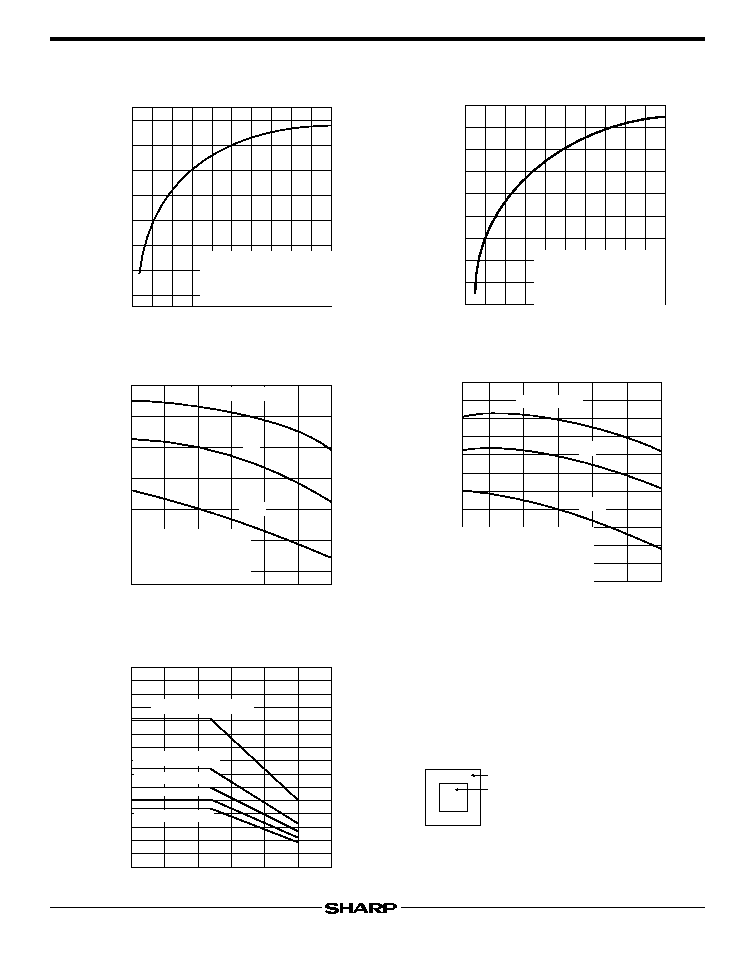
Fig.27 Output Peak Current vs. Dropout Voltage
(PQ05TZ51/PQ09TZ51/PQ12TZ51)
Fig.29 Output Peak Current vs. Junction Temperature
(PQ05TZ51/PQ09TZ51/PQ12TZ51)
Fig.31 Power Dissipation vs. Ambient
Temperature(Typical Value)
Fig.30 Output Peak Current vs. Junction Temperature
(PQ05TZ11/PQ09TZ11/PQ12TZ11)
Fig.28 Output Peak Current vs. Dropout Voltage
(PQ05TZ11/PQ09TZ11/PQ12TZ11)
Junction temperature T
j
(∞C)
Output peak current I
OP
(A)
0
25
50
75
100
125
-20
2.0
1.5
V
IN
-V
O
=2V
1V
0.5V
I
OP
:Output current when
output voltage is 95%
in comparison with
the initial value
Cu area 740mm
2
Cu area 180mm
2
Cu area 100mm
2
Cu area 70mm
2
Cu area 36mm
2
Power dissipation P
D
(W)
Ambient temperature T
a
(∞C)
-20
0
0
1
2
3
20
40
60
80
100
PWB
Material : Glass-cloth epoxy resin
Size : 50
X
50
X
1.6mm
Cu thickness : 35
µ
m
PWB
Cu
3
Low Power-Loss Voltage Regulators
PQ05TZ51/PQ05TZ11 Series
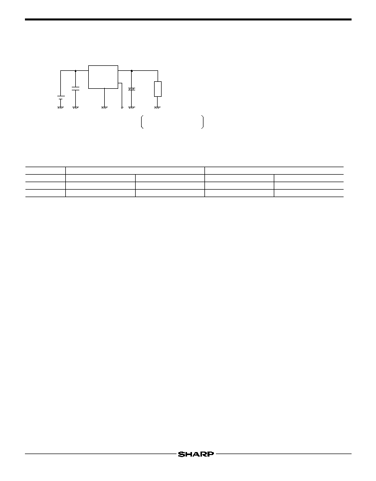
s
ON/OFF Operation
As shown in the figure, ON/OFF control function is available.
Sleeve-packaged products
Standard type
-
-
s
Model Line-ups for Tape-packaged Products
Tape-packaged products
High-precsion output type
PQ05TZ51 Series
PQ05TZ11 Series
Standard type
-
-
High-precsion output type
PQ05TZ5U Series
PQ05TZ1U Series
Output current
0.5A output
1.0A output
q
3
q
5
q
1
q
2
Load
V
O
V
IN
C
O
DC input
+
High : Output ON
Low or Open : Output OFF
ON/OFF
signal