PQ070XH01Z
PQ070XH01Z
s
Absolute Maximum Ratings
s
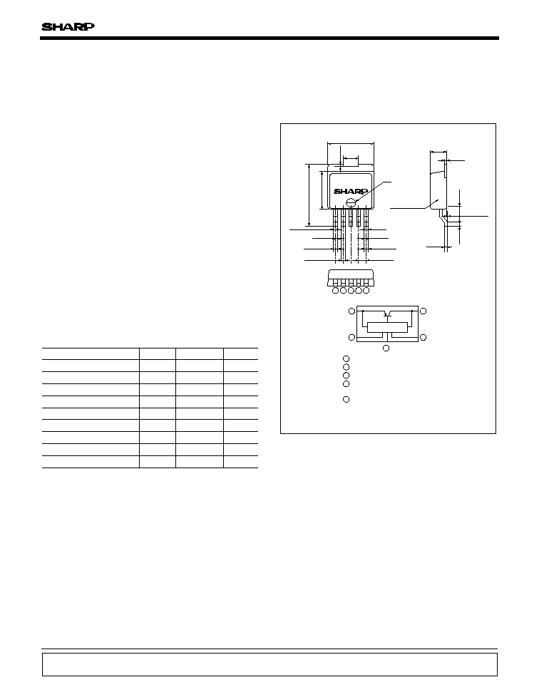
Outline Dimensions
(Unit : mm)
Parameter
Symbol
Rating
Unit
Input voltage
10
V
35
10
5
1
V
V
A
W
150
∞C
-
40 to
+
85
∞C
Junction temperature
Output adjustment terminal voltage
Output current
Output control voltage
V
IN
V
ADJ
I
O
V
C
T
j
(Ta
=
25
∞
C)
Operating temperature
Storage temperature
Soldering temperature
T
opr
-
40 to
+
150
∞C
T
stg
260 (10s)
∞C
T
sol
*1
*1
*1
*3
Power dissipation
P
D
*2
*1 All are open except GND and applicable terminals
*2 P
D
:With infinite heat sink
*3 Overheat protection may operate at the condition Tj
=
125∞C to 150∞C
1. Peripheral equipment of personal computers
2. Power supplies for various electronic equipment such as
DVD player or STB
s
Features
s
Applications
Low Voltage Operation Low
Power-loss Voltage Regulator
1. Low voltage operation (minimum operating voltage:2.35V)
2.5V input
available 1.5 to 1.8V
2. Large output current type (I
O
:1A)
3. Low dissipation current
(Dissipation current at no load:MAX.2mA
OFF-state dissipation current:MAX.5
µ
A)
4. Low power-loss
5. Built-in overcurrent and overheat protection functions
6. TO-263 package
PQ070XH01ZZ
:Sleeve-packaged product
PQ070XH01ZP
:Tape-packaged product
Notice
In the absence of confirmation by device specification sheets, SHARP takes no responsibility for any defects that may occur in equipment using any SHARP
devices shown in catalogs, data books, etc. Contact SHARP in order to obtain the latest device specification sheets before using any SHARP device.
Internet
Internet address for Electronic Components Group http://www.sharp.co.jp/ecg/
(2.4)
(
1.3)
0 to 0.25
0 7 0 X H 0 1
10.6
MAX.
2
3.28
±
0.5
(0.55)
8.4
±
0.5
13.7
MAX.
(0.6)
(0.6)
(0.6)
(0.45)
(0.45)
1.05
+
0.2
-
0.1
1.05
+
0.2
-
0.1
3
-
0.9
+
0.2
-
0.1
4
-
(1.7)
Epoxy resin
(0.6)
3.5
±
0.5
( ) : Typical dimensions
1
Output voltage adjustment
(V
ADJ
)
Specific IC
1
2
3
5
4
GND
DC output (V
O
)
DC input (V
IN
)
ON/OFF control (V
C
)
1
3
5
4
2
5
4
3
2
PQ070XH01Z
Parameter
Symbol
Conditions
V
IN
V
O
R
eg
L
R
eg
I
T
C
V
ref
RR
Unit
MAX.
TYP.
MIN.
-
-
-
-
45
-
-
I
O
=
5mA to 1A
V
IN
=
4 to 8V, I
O
=
5mA
T
j
=
0 to 125∞C, I
O
=
5mA
Refer to Fig.2
-
-
0.2
0.2
±
1.0
60
2
1
-
(Unless otherwise specified, condition shall be V
IN
=
5V, V
O
=
3V (R1
=
1k
), I
O
=
0.5A, V
C
=2.7V
,
Ta=25∞C)
V
V
%
%
%
dB
Input voltage range
Output voltage
Load regulation
V
ref
1.225
-
1.25
1.275
1.5
7
2.35
10
V
Reference voltage
Line regulation
Reference voltage temperature coefficient
Ripple Rejection
*4
Output on control voltage
Output off control voltage
Output off control current
Output off dissipation current
Output on control current
V
C (ON)
I
C (ON)
V
C (OFF)
I
C (OFF)
I
qs
-
-
-
-
-
-
-
-
I
O
=0A
I
O
=0A, V
C
=0.4V
I
O
=0A, V
C
=0.4V
2.0
-
-
200
0.8
2
-
V
µ
A
V
Dropout voltage
V
I-O
-
V
IN
=
2.85V, I
O
=
0.5A
-
0.5
V
µ
A
µ
A
-
5
Quiescent current
I
q
I
O
=0A
1
mA
-
2
*4 In case of opening control terminal , output voltage turns off
2
s
Electrical Characteristics
R
L
I
C
V
C
I
q
I
O
V
O
V
ref
+
0.33
µ
F
47
µ
F
R
1
R
2
1k
V
IN
A
A
A
3
4
5
2
1
V
V
V
O
=
V
ref
◊
(1
+
R
2
/R
1
)
.=.
1.25
◊
(1
+
R
2
/R
1
)
[R
1
=
1k
, V
ref
.=.
1.25V]
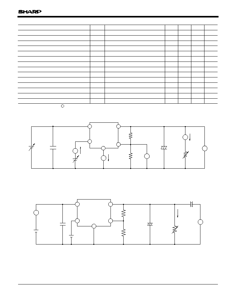
Fig.1
Standard Test Circuit
I
O
R
L
R
2
V
IN
V
ref
V
C
ei
eo
R
1
1k
2.7V
+
+
3
1
2
4
5
0.33
µ
F
47
µ
F
f
=
120Hz(sine wave)
ei(rms)
=
0.5V
V
O
=
3V(R
1
=
1k
)
V
IN
=
5V
I
O
=
0.3A
RR
=
20log(ei(rms)/eo(rms))
V
~
~
Fig.2
Test Circuit for Ripple Rejection
PQ070XH01Z
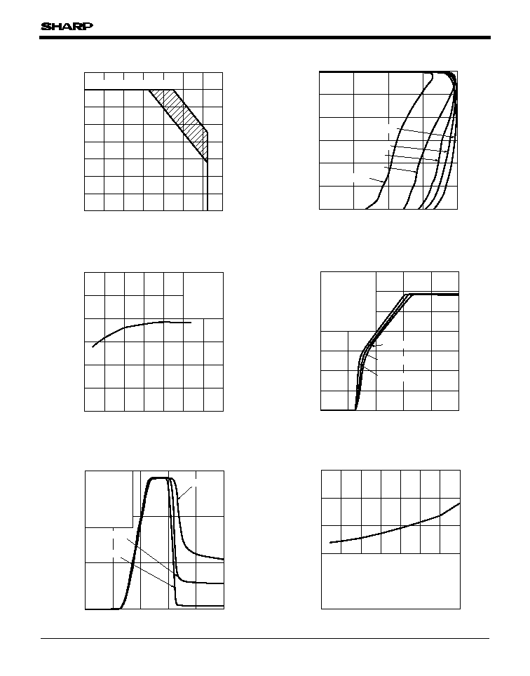
Fig.6 Output Voltage vs. Input Voltage
Fig.5 Reference Voltage vs. Ambient
Temperature
Fig.7 Circuit Operating Current vs. Input
Voltage
Fig.8 Dropout Voltage vs. Junction
Temperature
Reference voltage V
ref
(V)
1.23
1.235
1.24
1.245
1.25
1.255
1.26
-
50
-
25
0
25
50
75
100
125
Ambient temperature T
a
(
∞
C)
V
IN
=
4V
I
O
=
0.5A
V
C
=
2.7V
R
1
=
1k
R
2
=
1.4k
Circuit operating current I
BIAS
(mA)
Input voltage V
IN
(V)
0
10
20
30
0
1
2
3
4
5
R
L
=
3
(I
O
=
1A)
R
L
=
6
(I
O
=
0.5A)
R
L
=
(I
O
=
0A)
V
C
=
2.7V
T
a
=
Room temp.
R
1
=
1k
R
2
=
1.4k
(V
O
=
3V)
C
IN
=
0.33
µ
F
C
O
=
47
µ
F
Output voltage V
O
(V)
Input voltage V
IN
(V)
0
0.5
1
1.5
2
2.5
3
3.5
0
1
2
3
4
5
R
L
=
(I
O
=
0.3A)
R
L
=
3
(I
O
=
1A)
R
L
=
6
(I
O
=
0.5A)
V
C
=
2.7V
T
a
=
Room temp.
R
1
=
1k
R
2
=
1.4k
(V
O
=
3V)
C
IN
=
0.33
µ
F
C
O
=
47
µ
F
Dropout voltage V
I-O
(V)
0
0.05
0.1
0.15
0.2
0.25
-
50
-
25
0
25
50
75
100
125
Junction temperature T
j
(
∞
C)
V
IN
:Input voltage shall be the value when output
voltage is 95% in camparison with the initial
value
I
O
=
0.5A
V
C
=
2.7V
R
1
=
1k
R
2
=
1.4k
(V
O
=
3V)
Power dissipation P
D
(W)
0
5
10
15
20
25
30
35
40
-
40
-
20
0
20
40
60
80
100
P
D
: With infinite heat sink
Ambient temperature T
a
(
∞
C)
Note) Oblique line prtion:Overheat protection may operate in this area
Output voltage V
O
(V)
Output current I
O
(A)
0
0.5
1
1.5
2
2.5
3
0
0.5
1
1.5
2
V
O
=
3V
V
IN
=
10V
V
IN
=
7V
V
IN
=
5.5V
V
IN
=
5V
V
IN
=
4.5V
Fig.3 Power Dissipation vs. Ambient
Temperature
Fig.4 Overcurrent Protection Characteristics
PQ070XH01Z
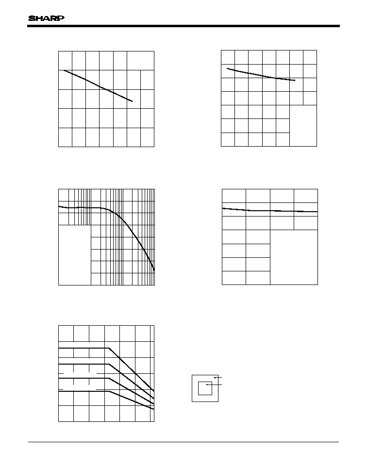
Fig.12 Ripple Rejection vs. Output Current
Fig.11 Ripple Rejection vs. Input Ripple
Frequency
Ripple rejection RR (dB)
0.1
1
10
100
Input ripple frequency f (kHz)
35
40
45
50
55
60
65
70
75
ei(rms)
=
0.5V
V
IN
=
5V
V
C
=
2.7V
I
O
=
0.3A
C
O
=
47
µ
F
T
a
=
Room temp.
R
1
=
1k
R
2
=
1.4k
(V
O
=
3V)
40
45
50
55
60
65
70
75
0
0.25
0.5
0.75
1
Ripple rejection RR (dB)
Output current I
O
(A)
ei (rms)
=
0.5V
f
=
120Hz
V
IN
=
5V
V
C
=
2.7V
C
O
=
47
µ
F
T
a
=
Room temp.
R
1
=
1k
R
2
=
1.4k
(V
O
=
3V)
ON-OFF threshold voltage V
C
(ON/OFF) (V)
0
0.5
1
1.5
2
2.5
-
50
-
25
0
25
50
75
100
125
Ambient temperature T
a
(
∞
C)
V
IN
=
2.5V
I
O
=
0A
Quiescent current I
q
(mA)
-
50
-
25
0
25
50
75
100
125
Ambient temperature T
a
(
∞
C)
0
0.2
0.4
0.6
0.8
1
1.2
1.4
V
IN
=
4V
I
O
=
0A
V
C
=
2.7V
R
1
=
1k
R
2
=
1.4k
(V
O
=
3V)
Fig.9 ON-OFF Threshold Voltage vs.
Ambient Temperature
Fig.10 Quiescent Current vs. Ambient
Temperature
Power dissipation P
D
(W)
0
1
2
3
4
5
6
-
40
-
20
0
20
40
60
80
Ambient temperature T
a
(
∞
C)
Cu area 3 600mm
2
Cu area 900mm
2
Cu area 400mm
2
Cu area 115mm
2
Material : Glass-cloth epoxy resin
Size : 60
◊
60
◊
1.6mm
Cu thickness : 65
µ
m
PWB
PWB
Cu
Fig.13 Power Dissipation vs. Ambient
Temperature
PQ070XH01Z
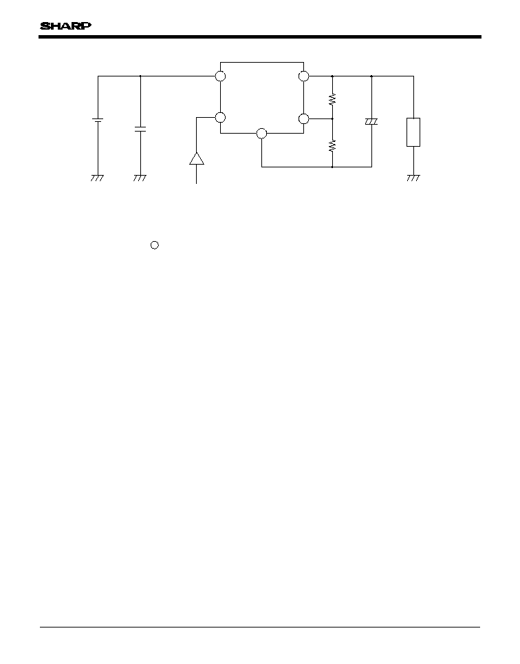
Fig.15 Example of Application
1
3
2
5
4
V
O
V
IN
R
2
C
IN
R
1
1k
C
O
+
Load
ON/OFF signal
High:Output ON
Low or open Output OFF
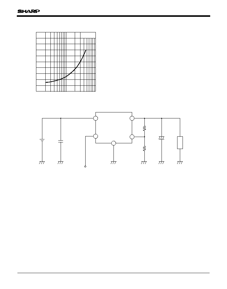
Fig.14 Output Voltage vs. R2 (Typical Value)
Output voltage V
O
(V)
R
2
(
)
0
1
2
3
4
5
6
7
8
9
10
100
1 000
10 000
R
1
=
1k
PQ070XH01Z
s
Precautions for Use
1
3
2
5
4
V
IN
C
IN
R
2
R
1
C
O
V
O
+
C-MOS or TTL
Load
1. External connection
(1) The connecting wiring of C
O,
C
IN
and each terminal, fin portion must be as short as possible. It may oscillate by type, value and
wiring condition of capacitor. Confirm the output wareform in actual using condition beforehand.
(2) ON/OFF control terminal is compatible with LS-TTL. It enables to be direcrly driven by TTL or C-MOS standard logic
(RCA4000 series).
(3) If voltage is applied under the conditions that device pin is connected divergently or reversely, the deterioration of
characteristics or damage may occur. Never allow improper mounting.
2. Thermal protection design
Power dissipation of devices is obtained by the following equation.
P
D
=
I
O
◊
(V
IN
-
V
O
)
+
V
IN
◊
I
q
When ambient temperature T
a
and power dissipation P
D
during operation are determined, operate element within the safety
operation area specified by the derating curve. Insufficient radiation gives an unfavorable influence to the normal operation and
reliability of the device.
In the external area of the safety operation area shown by the derating curve, the overheat protection circuit may operate to shut-
down output. However please avoid keeping such condition for a long time.
3. ESD (Electrostatic Sensitivity Discharge)
Be careful not to apply electrostatic discharge to the device since this device employs a bipolar IC and may be damaged by electro
static discharge. Followings are some methods against excessive voltage caused by electro static discharge.
(1) Human body must be grounded to discharge the electro charge which is charged in the body or cloth.
(2) Anything that is in contact with the device such as workbench, inserter, or measuring instrument must be grounded.
(3) Use a soldering dip basin with a minimum leak current (isolation resistance 10M
or more) from the AC power supply line.
Also the soldering dip basin must be grounded.
2
PQ070XH01Z
s
Output Voltage Fine Tuning
1. Connecting external resistors R
1
and R
2
to terminals , , allows the output voltage to be fine tuned from 1.5V to 7V. Refer to
the figure below and Fig.14 when connecting external resistors for fine tuning output voltage.
4
5
3
R
2
R
1
V
O
V
ref
+
-
V
O
=
V
ref
◊
(1
+
R
2
/R
1
)
.=.
1.25
◊
(1
+
R
2
/1 000)
[R
1
=
1k
, V
ref
.=.
1.25V]
3
4
5

115
Application Circuits
NOTICE
qThe circuit application examples in this publication are provided to explain representative applications of
SHARP devices and are not intended to guarantee any circuit design or license any intellectual property
rights. SHARP takes no responsibility for any problems related to any intellectual property right of a
third party resulting from the use of SHARP's devices.
qContact SHARP in order to obtain the latest device specification sheets before using any SHARP device.
SHARP reserves the right to make changes in the specifications, characteristics, data, materials,
structure, and other contents described herein at any time without notice in order to improve design or
reliability. Manufacturing locations are also subject to change without notice.
qObserve the following points when using any devices in this publication. SHARP takes no responsibility
for damage caused by improper use of the devices which does not meet the conditions and absolute
maximum ratings to be used specified in the relevant specification sheet nor meet the following
conditions:
(i) The devices in this publication are designed for use in general electronic equipment designs such as:
--- Personal computers
--- Office automation equipment
--- Telecommunication equipment [terminal]
--- Test and measurement equipment
--- Industrial control
--- Audio visual equipment
--- Consumer electronics
(ii)Measures such as fail-safe function and redundant design should be taken to ensure reliability and
safety when SHARP devices are used for or in connection with equipment that requires higher
reliability such as:
--- Transportation control and safety equipment (i.e., aircraft, trains, automobiles, etc.)
--- Traffic signals
--- Gas leakage sensor breakers
--- Alarm equipment
--- Various safety devices, etc.
(iii)SHARP devices shall not be used for or in connection with equipment that requires an extremely
high level of reliability and safety such as:
--- Space applications
--- Telecommunication equipment [trunk lines]
--- Nuclear power control equipment
--- Medical and other life support equipment (e.g., scuba).
qContact a SHARP representative in advance when intending to use SHARP devices for any "specific"
applications other than those recommended by SHARP or when it is unclear which category mentioned
above controls the intended use.
qIf the SHARP devices listed in this publication fall within the scope of strategic products described in the
Foreign Exchange and Foreign Trade Control Law of Japan, it is necessary to obtain approval to export
such SHARP devices.
qThis publication is the proprietary product of SHARP and is copyrighted, with all rights reserved. Under
the copyright laws, no part of this publication may be reproduced or transmitted in any form or by any
means, electronic or mechanical, for any purpose, in whole or in part, without the express written
permission of SHARP. Express written permission is also required before any use of this publication
may be made by a third party.
qContact and consult with a SHARP representative if there are any questions about the contents of this
publication.