65
Low Power-Loss Voltage Regulators
PQ05DZ51/11 Series / PQ3DZ53/13
s
Features
q
Low power-loss
(Dropout voltage : MAX. 0.5V)
q
Surface mount package (equivalent to SC-63)
q
Available 3.3V, 5V, 9V, 12V output type
q
Output current (0.5A :
PQ05DZ51 series/PQ3DZ53
)
(1.0A :
PQ05DZ11 series/PQ3DZ13
)
q
Output voltage precision : �3.0%
q
Built-in ON/OFF control function
q
Low dissipation current at OFF-state (Iqs : MAX. 5�A)
q
Built-in overcurrent protection, overheat protection
function, ASO protection function
q
Available tape-packaged products
(�330mm reel : 3 000 pcs.,
PQ05DZ5U/1U
series,
PQ3DZ53U/13U
)
s
Applications
q
Personal computers
q
CD-ROM drives
q
Power supplies for various OA equipment
s
Model Line-ups
s
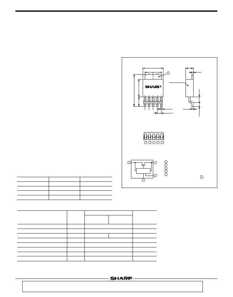
Outline Dimensions
(Unit : mm)
0.5A/1.0A Output, General Purpose, Surface Mount Type Low Power-Loss Voltage Regulator
� Please refer to the chapter " Handling Precautions ".
PQ05DZ51/11 Series / PQ3DZ53/13
s
Absolute Maximum Ratings
Parameter
Symbol
Rating
f1
All are open except GND and applicable terminals.
f2
P
D
: With infinite heat sink
f3
Overheat protection may operate at 125<=Tj<=150�C
Unit
(T
a
=25�C)
f1
f1
f3
f2
Output current
Input voltage
ON/OFF control terminal voltage
Power dissipation
Junction temperature
Operating temperature
Storage temperature
Soldering temperature
V
IN
Vc
Io
P
D
T
j
T
opr
T
stg
T
sol
PQ05DZ51 series
PQ3DZ53
PQ05DZ11 series
PQ3DZ13
24
24
8
150
-20 to + 80
-40 to +150
260 (for 10s)
0.5
1.0
V
V
A
W
�C
�C
�C
�C
05DZ11
0.5
�
0.2
0.1
Epoxy resin
0.5
1.7
0.5
0.9
5.2 0.5
9.7
MAX.
5.5
0.5
2.5
MIN.
2.3 0.5
4
1.27
6.6 MAX.
�
�
�
�
(
)
(
)
()
()
(
)
3
1
1
3
1
2
3
3
4
5
5
2
2
3
4
5
Internal connection diagram
NC
GND
DC input(V
IN
)
DC output(Vo)
ON/OFF control terminal(Vc)
Heat sink is common to terminal
(Vo)
Specific IC
5.0V output
9.0V output
12.0V output
3.3V output
0.5A output
1.0A output
PQ3DZ53
PQ3DZ13
PQ05DZ11
PQ09DZ11
PQ12DZ11
PQ05DZ51
PQ09DZ51
PQ12DZ51
Notice
In the absence of confirmation by device specification sheets,SHARP takes no responsibility for any defects that may occur in equipment using any SHARP
devices shown in catalogs,data books,etc.Contact SHARP in order to obtain the latest device specification sheets before using any SHARP device.
Internet Internet address for Electronic Components Group http://www.sharp.co.jp/ecg/
66
Low Power-Loss Voltage Regulators
PQ05DZ51/11 Series / PQ3DZ53/13
s
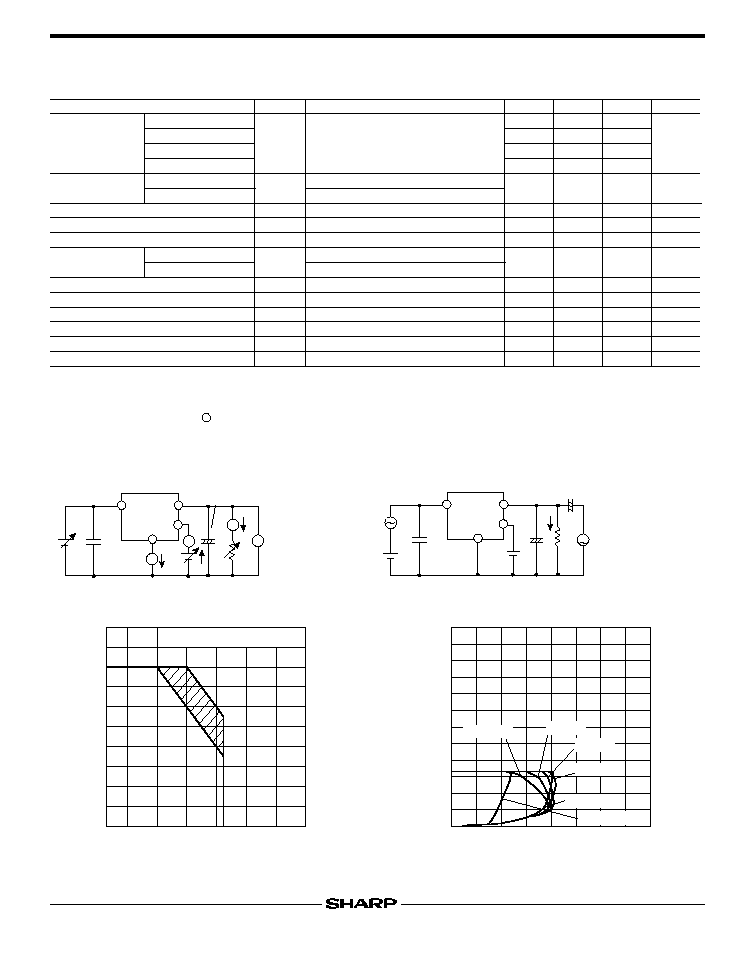
Electrical Characteristics
Fig. 3 Power Dissipation vs. Ambient
Temperature
Fig. 4 Overcurrent Protection Characteristics
(Typical Value) (PQ3DZ53)
Fig. 1 Test Circuit
Fig. 2 Test Circuit of Ripple Rejection
Parameter
Symbol
Conditions
MIN.
TYP.
MAX.
Unit
4.85
5.0
5.15
V
��
f8
0.2
f8
0.1
2.0
%
��
2.5
%
f9
�
0.01
��
��
%/�C
45
dB
��
f8
0.2
60
0.5
V
2.0
V
��
��
0.8
V
��
f8
4
��
��
10
5
��
��
��
��
��
mA
2
�
A
�
A
�
A
200
f4
PQ3DZ53/PQ3DZ13
:V
IN
=5V,
PQ05DZ51/11
:V
IN
=7V,
PQ09DZ51/11
:V
IN
=11V,
PQ12DZ51/11
: V
IN
=14V
f5
PQ3DZ53/13
:V
IN
=4 to 10V,
PQ05DZ51/11
:V
IN
= 6 to 16V,
PQ09DZ51/11
:V
IN
=10 to 20V,
PQ12DZ51/11
: V
IN
=13 to 23V
f6
Input voltage shall be the value when output voltage is 95% in comparison with the initial value.
PQ3DZ53/13
:V
IN
=3.7V
f7
In case of opening control terminal , output voltage turns off.
f8
Applied only to
PQ05DZ51/11
series.
f9
PQ3DZ53/PQ3DZ13
:
�
0.02
11.64
12.0
12.36
��
(Unless otherwise specified, conditions shall be Vc=2.7V, Io=0.3A[
PQ05DZ51 series/PQ3DZ53
], Io=0.5A[
PQ05DZ11 series/PQ3DZ13
]
f4
, T
a
=25�C)
3.201
3.3
3.399
8.73
9.0
9.27
��
2
PQ3DZ53/PQ3DZ13
PQ05DZ51/PQ05DZ11
PQ05DZ51 series
PQ05DZ11 series
PQ09DZ51/PQ09DZ11
PQ12DZ51/PQ12DZ11
PQ05DZ51 series/PQ3DZ53
PQ05DZ11 series/PQ3DZ13
Dropout voltage
Output voltage
Load regulation
Ripple rejection
Line regulation
Temperature coefficient of output voltage
ON-state current for control
f7
ON-state voltage for control
OFF-state voltage for control
OFF-state current for control
Quiescent current
Output OFF-state consumption current
Vo
R
eg
L
R
eg
I
TcVo
RR
V
i-o
Vc
(ON)
Vc
(OFF)
I
q
I
qs
Ic
(ON)
Ic
(OFF)
Io=5mA to 0.5A,
f4
Io=5mA to 1.0A,
f4
f5
, Io=5mA
Tj=0 to 125�C, Io=5mA,
f4
f6
, Io=0.3A
f6
, Io=0.5A
Vc=0.4V, Io=0A,
f4
V
C
=0.4V, Io=0A,
f4
Refer to Fig.2
f4
Io=0A,
f4
f4
f4
Io=0A,
f4
V
e
i
V
IN
Io
e
o
R
L
0.33
�
F
47
�
F
+
+
f=120Hz(sine wave)
e
i
=0.5V
rms
V
IN
=5V(
PQ3DZ53/13
)
7V(
PQ05DZ51/11
)
11V(
PQ09DZ51/11
)
14V(
PQ12DZ51/11
)
Io=0.3A
RR=20 log(e
i
/e
o
)
2.7V
5
2
3
1
A
V
A
A
V
IN
Iq
Ic
Io
Vo
Vc
R
L
0.33
�
F
47
�
F
+
1
3
2
5
0
�20 0
P
D
P
D
:With infinite heat sink
80
50
100
150
0.5
1.0
8
Power dissipation P
D
(W)
Ambient temperature T
a
(�C)
Output voltage Vo
(V)
Output current Io (A)
0
0.5
1.5
2.0
1.0
1
2
3
4
7
8
9
5
6
10
11
12
V
i
-
O
=10V
V
i
-
O
=2V
V
i
-
O
=1V
V
i
-
O
=0.5V
V
i
-
O
=5V
V
i
-
O
=3V
Note) Oblique line portion : Overheat protection may operate in this area.
67
Low Power-Loss Voltage Regulators
PQ05DZ51/11 Series / PQ3DZ53/13
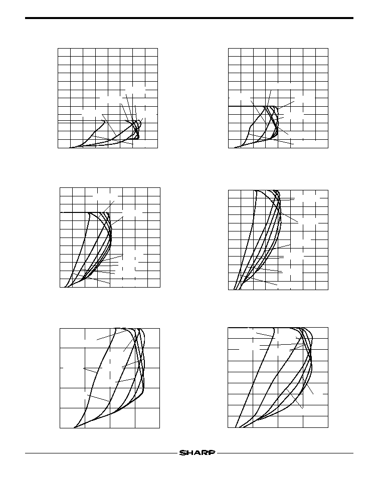
Fig. 5 Overcurrent Protection Characteristics
(Typical Value) (PQ3DZ13)
Output voltage Vo
(V)
Output current Io
(A)
0
0.5
1.5
2.0
1.0
1
2
3
4
7
8
9
5
6
10
11
12
V
i
-
O
=3V
V
i
-
O
=1V
V
i
-
O
=2V
V
i
-
O
=0.5V
V
i
-
O
=10V
V
i
-
O
=5V
Fig. 6 Overcurrent Protection Characteristics
(Typical Value) (PQ05DZ51)
Output voltage Vo
(V)
Output current Io (A)
0
0.5
1.5
2.0
1.0
1
2
3
4
7
8
9
5
6
10
11
12
V
i
-
O
=10V
V
i
-
O
=2V
V
i
-
O
=0.5V
V
i
-
O
=5V
V
i
-
O
=3V
V
i
-
O
=1V
Fig. 7 Overcurrent Protection Characteristics
(Typical Value) (PQ09DZ51)
Fig. 8 Overcurrent Protection Characteristics
(Typical Value) (PQ12DZ51)
Output voltage Vo
(V)
Output current Io
(A)
0
0.5
1.5
2.0
1.0
1
2
3
4
7
8
9
5
6
10
11
12
V
i
-
O
=10V
V
i
-
O
=2V
V
i
-
O
=1V
V
i
-
O
=0.5V
V
i
-
O
=5V
V
i
-
O
=3V
Output voltage Vo
(V)
Output current Io
(A)
0
0.5
1.5
2.0
1.0
1
2
3
4
7
8
9
5
6
10
11
12
V
i
-
O
=10V
V
i
-
O
=2V
V
i
-
O
=1V
V
i
-
O
=0.5V
V
i
-
O
=5V
V
i
-
O
=3V
Fig. 9 Overcurrent Protection Characteristics
(Typical Value)(PQ05DZ11)
Output current Io
(A)
Output voltage Vo
(V)
1.0
1.5
2.0
0.5
0
1.0
2.0
3.0
4.0
5.0
Vi-o=0.5V
Vi-o=1V
Vi-o=2V
Vi-o=3V
Vi-o=5V
Vi-o=10V
Fig.10 Overcurrent Protection Characteristics
(Typical Value)(PQ09DZ11)
Output current Io
(A)
Output voltage Vo
(V)
0
0.5
1.0
1.5
2.0
1.0
2.0
3.0
4.0
5.0
7.0
8.0
6.0
9.0
Vi-o=10V
Vi-o=5V
Vi-o=0.5V
Vi-o=1V
Vi-o=2V
Vi-o=3V
68
Low Power-Loss Voltage Regulators
PQ05DZ51/11 Series / PQ3DZ53/13
Output voltage deviation
Vo
(mV)
Junction temperature T
j
(�C)
�25
0
0
�
50
�
45
�
40
�
35
�
30
�
25
�
20
�
15
�
10
�
5
5
10
15
20
25
30
35
25
50
75
100
125
V
IN
=7V , Io=0.3A , Vc=2.7V
(
PQ05DZ51
)
V
IN
=7V , Io=0.5A , Vc=2.7V
(
PQ05DZ11
)
PQ05DZ51
PQ05DZ11
Output voltage deviation
Vo
(mV)
Junction temperature T
j
(�C)
�25
0
0
�
50
�
45
�
40
�
35
�
30
�
25
�
20
�
15
�
10
�
5
5
10
15
20
25
30
35
25
50
75
100
125
V
IN
=5V , Io=0.3A , Vc=2.7V
(
PQ3DZ53
)
V
IN
=5V , Io=0.5A , Vc=2.7V
(
PQ3DZ13
)
PQ3DZ13
PQ3DZ53
Fig.13 Output Voltage Deviation vs. Junction
Temperature (PQ3DZ53/13)
Fig.14 Output Voltage Deviation vs. Junction
Temperature (PQ05DZ51/11)
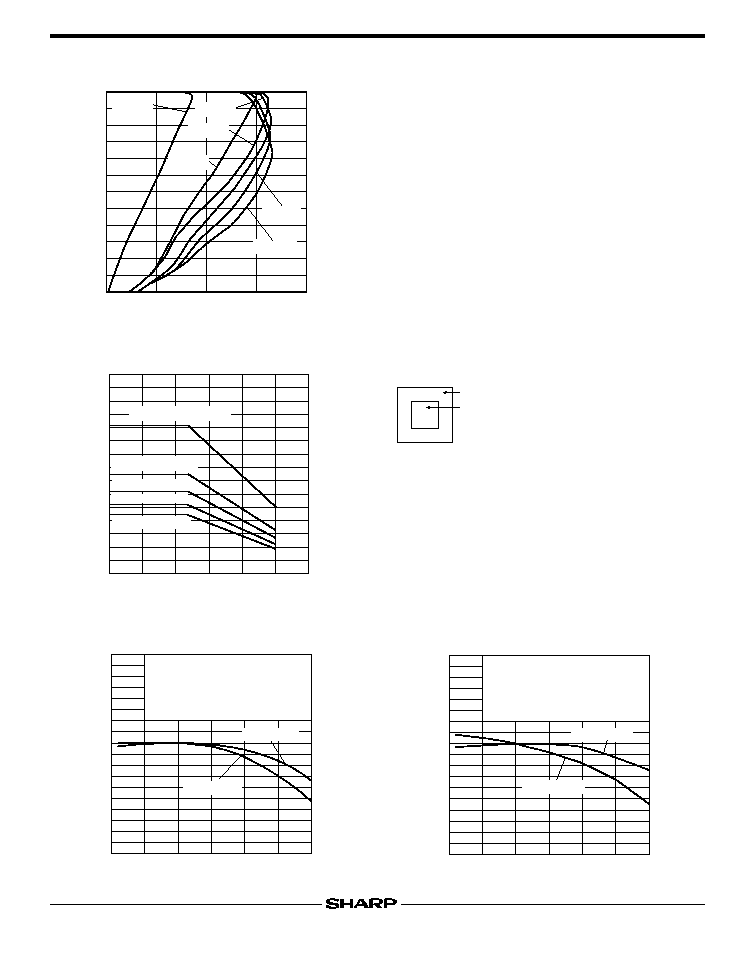
Fig.11 Overcurrent Protection characteristics
(Typical Value)(PQ12DZ11)
Output current Io
(A)
Output voltage Vo
(V)
0
0.5
1.0
1.5
2.0
1
2
3
4
5
7
8
6
9
10
11
12
Vi-o=10V
Vi-o=5V
Vi-o=2V
Vi-o=3V
Vi-o=1V
Vi-o=0.5V
Fig.12 Power Dissipation vs. Ambient
Temperature (Typical Value)
PWB
Material : Glass-cloth epoxy resin
Size : 50 x 50 x 1.6mm
Cu thickness : 35
�
m
PWB
Cu
3
Cu area 740mm
2
Cu area 180mm
2
Cu area 100mm
2
Cu area 70mm
2
Cu area 36mm
2
Power dissipation P
D
(W)
Ambient temperature T
a
(�C)
�20
0
0
1
2
3
20
40
60
80
100
69
Low Power-Loss Voltage Regulators
PQ05DZ51/11 Series / PQ3DZ53/13
Output voltage Vo
(V)
Input voltage V
IN
(V)
10
0
5
15
10
5
15
Vc=2.7V , C
i
=0.33
�
F , Co=47
�
F
T
j
=25�C
R
L
=24
R
L
=40
R
L
=
Output voltage Vo (V)
Input voltage V
IN
(V)
0
5
15
10
5
15
Vc=2.7V , C
i
=0.33
�
F , Co=47
�
F
T
j
=25�C
R
L
=30
R
L
=18
R
L
=
10
Fig.19 Output Voltage vs. Input Voltage
(Typical Value) (PQ09DZ51)
Fig.20 Output Voltage vs. Input Voltage
(Typical Value) (PQ12DZ51)
Output voltage Vo
(V)
Input voltage V
IN
(V)
0
1
2
3
4
5
6
7
8
1
2
3
4
5
6
7
Vc=2.7V , C
i
=0.33
�
F , Co=47
�
F
R
L
=16.7
R
L
=10
R
L
=
Output voltage Vo
(V)
Input voltage V
IN
(V)
0
1
2
3
4
5
6
7
8
1
2
3
4
5
6
7
Vc=2.7V , C
i
=0.33
�
F , Co=47
�
F
R
L
=11
R
L
=6.6
R
L
=
Fig.17 Output Voltage vs. Input Voltage
(Typical Value) (PQ3DZ53)
Fig.18 Output Voltage vs. Input Voltage
(Typical Value) (PQ05DZ51)
Output voltage deviation
Vo(mV)
Junction temperature T
j
(�C)
�
25
0
0
�90
�80
�70
�60
�50
�40
�30
�20
�10
10
20
30
40
50
60
70
25
50
75
100
125
V
IN
=14V , Io=0.3A , Vc=2.7V
(
PQ12DZ51
)
V
IN
=14V , Io=0.5A , Vc=2.7V
(
PQ12DZ11
)
PQ12DZ11
PQ12DZ51
Fig.16 Output Voltage Deviation vs. Junction
Temperature (PQ12DZ51/11)
�25
0
0
�
90
�
80
�
70
�
60
�
50
�
40
�
30
�
20
�
10
10
20
30
40
50
60
70
25
50
75
100
125
Output voltage deviation
Vo
(mV)
Junction temperature T
j
(�C)
V
IN
=11V , Io=0.3A , Vc=2.7V
(
PQ09DZ51
)
V
IN
=11V , Io=0.5A , Vc=2.7V
(
PQ09DZ11
)
PQ09DZ11
PQ09DZ51
Fig.15 Output Voltage Deviation vs. Junction
Temperature (PQ09DZ51/11)
70
Low Power-Loss Voltage Regulators
PQ05DZ51/11 Series / PQ3DZ53/13
Input voltage V
IN
(V)
Circuit operating current I
BIAS
(mA)
0
1
2
3
4
5
6
7
8
5
0
20
10
15
R
L
=16.7
R
L
=10
R
L
=
Vc=2.7V , C
i
=0.33
�
F
,
Co=47
�
F
Input voltage V
IN
(V)
Circuit operating current I
BIAS
(mA)
0
1
2
3
4
5
6
7
8
5
0
20
10
15
Vc=2.7V , C
i
=0.33
�
F
,
Co=47
�
F
R
L
=11
R
L
=6.6
R
L
=
Fig.25 Circuit Operating Current vs. Input
Voltage (PQ3DZ53)
Fig.26 Circuit Operating Current vs. Input
Voltage (PQ05DZ51)
Output voltage Vo
(V)
Input voltage V
IN
(V)
10
0
5
15
10
5
15
Vc=2.7V , C
i
=0.33
�
F , Co=47
�
F
T
j
=25�C
R
L
=12
R
L
=24
R
L
=
Output voltage Vo
(V)
Input voltage V
IN
(V)
10
0
5
15
10
5
15
Vc=2.7V , C
i
=0.33
�
F , Co=47
�
F
T
j
=25�C
R
L
=9
R
L
=18
R
L
=
Fig.23 Output Voltage vs. Input Voltage
(Typical Value) (PQ09DZ11)
Fig.24 Output Voltage vs. Input Voltage
(Typical Value) (PQ12DZ11)
Output voltage Vo
(V)
Input voltage V
IN
(V)
0
1
2
3
4
5
6
7
8
1
2
3
4
5
6
7
8
Vc=2.7V , C
i
=0.33
�
F , Co=47
�
F
T
j
=25�C
R
L
=5
R
L
=10
R
L
=
Fig.22 Output Voltage vs. Input Voltage
(Typical Value) (PQ05DZ11)
Output voltage Vo
(V)
Input voltage V
IN
(V)
0
1
2
3
4
5
6
7
8
1
2
3
4
5
6
7
8
Vc=2.7V , C
i
=0.33
�
F , Co=47
�
F
T
j
=25�C
R
L
=6.6
R
L
=
R
L
=3.3
Fig.21 Output Voltage vs. Input Voltage
(Typical Value) (PQ3DZ13)
71
Low Power-Loss Voltage Regulators
PQ05DZ51/11 Series / PQ3DZ53/13
Fig.31 Circuit Operating Current vs. Input
Voltage (PQ09DZ11)
Input voltage V
IN
(V)
Circuit operating current I
BIAS
(mA)
0
5
10
15
10
20
30
Vc=2.7V , C
i
=0.33
�
F, Co=47
�
F
R
L
=18
R
L
=9
R
L
=
Fig.32 Circuit Operating Current vs. Input
Voltage (PQ12DZ11)
Input voltage V
IN
(V)
Circuit operating current I
BIAS
(mA)
0
5
10
15
10
20
30
Vc=2.7V , C
i
=0.33
�
F, Co=47
�
F
R
L
=24
R
L
=12
R
L
=
Fig.29 Circuit Operating Current vs. Input
Voltage (PQ3DZ13)
Input voltage V
IN
(V)
Circuit operating current I
BIAS
(mA)
0
1
2
3
4
5
6
7
8
10
20
30
Vc=2.7V , C
i
=0.33
�
F, Co=47
�
F
R
L
=6.6
R
L
=3.3
R
L
=
Fig.30 Circuit Operating Current vs. Input
Voltage (PQ05DZ11)
Input voltage V
IN
(V)
Circuit operating current I
BIAS
(mA)
0
1
2
3
4
5
6
7
8
10
20
30
Vc=2.7V , C
i
=0.33
�
F, Co=47
�
F
R
L
=10
R
L
=5
R
L
=
Input voltage V
IN
(V)
Circuit operating current I
BIAS
(mA)
0
5
10
15
5
0
10
15
20
Vc=2.7V , C
i
=0.33
�
F , Co=47
�
F
R
L
=40
R
L
=24
R
L
=
Fig.28 Circuit Operating Current vs. Input
Voltage (PQ12DZ51)
Input voltage V
IN
(V)
Circuit operating current I
BIAS
(mA)
0
5
10
15
5
0
10
15
20
Vc=2.7V , C
i
=0.33
�
F , Co=47
�
F
R
L
=30
R
L
=18
R
L
=
Fig.27 Circuit Operating Current vs. Input
Voltage (PQ09DZ51)
72
Low Power-Loss Voltage Regulators
PQ05DZ51/11 Series / PQ3DZ53/13
Fig.37 Ripple Rejection vs. Input Ripple
Frequency (PQ05DZ51series/PQ3DZ53)
Ripple rejection RR (dB)
Input ripple frequency f
(kHz)
RR=20log (e
i
/e
0
)
Io=0.3A, T
j
=25�C
e
i
=0.5V
rms
(sine wave)
0.1
1
10
100
40
45
50
55
60
65
70
75
80
V
IN
=5V (
PQ3DZ53
)
=7V (
PQ05DZ51
)
=11V (
PQ09DZ51
)
=14V (
PQ12DZ51
)
PQ3DZ53
PQ05DZ51
PQ09DZ51
PQ12DZ51
Fig.38 Ripple Rejection vs. Input Ripple
Frequency (PQ05DZ11series/PQ3DZ13)
Ripple rejection RR (dB)
Input ripple frequency f
(kHz)
RR=20log (e
i
/e
0
)
Io=0.3A, T
j
=25�C
e
i
=0.5V
rms
(sine wave)
0.1
1
10
100
40
45
50
55
60
65
70
75
80
V
IN
=5V (
PQ3DZ13
)
=7V (
PQ05DZ11
)
=11V (
PQ09DZ11
)
=14V (
PQ12DZ11
)
PQ12DZ11
PQ09DZ11
PQ05DZ11
PQ3DZ13
Fig.35 Quiescent Current vs. Junction
Temperature (PQ05DZ51series/PQ3DZ53)
Junction temperature T
j
(�C)
Quiescent current Iq
(mA)
0
25
50
75
100
125
�25
2.5
3
3.5
4
4.5
5
V
IN
=7V (
PQ05DZ51
)
V
IN
=5V (
PQ3DZ53
)
V
IN
=11V (
PQ09DZ51
)
V
IN
=14V (
PQ12DZ51
)
Io=0A
Vc=2.7V
PQ12DZ51
PQ05DZ51
PQ3DZ53
PQ09DZ51
Junction temperature T
j
(�C)
Quiescent current Iq
(mA)
0
25
50
75
100
125
�25
3.4
3.6
3.8
4.0
4.2
4.4
V
IN
=7V (
PQ05DZ11
)
V
IN
=5V (
PQ3DZ13
)
V
IN
=11V (
PQ09DZ11
)
V
IN
=14V (
PQ12DZ11
)
Io=0A
Vc=2.7V
PQ12DZ11
PQ09DZ11
PQ05DZ11
PQ3DZ13
Fig.36 Quiescent Current vs. Junction
Temperature (PQ05DZ11series/PQ3DZ13)
Fig.34 Dropout Voltage vs. Junction
Temperature (PQ05DZ11series/PQ3DZ13)
Junction temperature T
j
(�C)
Dropout voltage V
i
�O
(V)
�20
0
20
40
60
80 100 120
0.10
0.11
0.12
0.13
0.14
0.16
0.17
0.15
0.18
PO05DZ11
:V
IN
=4.75V, Io=0.5A, Vc=2.7V
PO09DZ11
:V
IN
=8.55V, Io=0.5A, Vc=2.7V
PO12DZ11
:V
IN
=11.4V, Io=0.5A, Vc=2.7V
PO3DZ13
:V
IN
=3.135V, Io=0.5A, Vc=2.7V
PQ12DZ11
PQ09DZ11
PQ3DZ13
PQ05DZ11
Fig.33 Dropout Voltage vs. Junction
Temperature (PQ05DZ51series/PQ3DZ53)
Junction temperature T
j
(�C)
Dropout voltage V
i
�O
(V)
�20
0
20
40
60
80 100 120
0.10
0.11
0.12
0.13
0.14
0.16
0.20
0.19
0.17
0.15
0.18
PO05DZ51
:V
IN
=4.75V, Io=0.3A, Vc=2.7V
PO09DZ51
:V
IN
=8.55V, Io=0.3A, Vc=2.7V
PO12DZ51
:V
IN
=11.4V, Io=0.3A, Vc=2.7V
PO3DZ53
:V
IN
=3.135V, Io=0.3A, Vc=2.7V
PQ3DZ53
PQ05DZ51
PQ09DZ51
PQ12DZ51
73
Low Power-Loss Voltage Regulators
PQ05DZ51/11 Series / PQ3DZ53/13
s
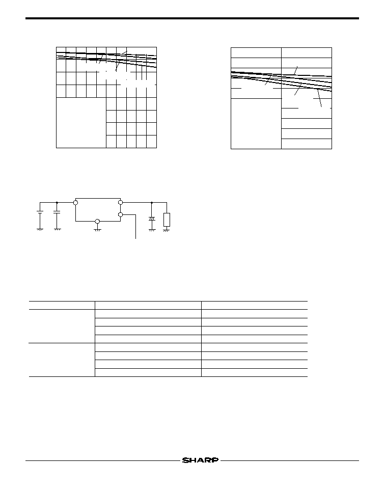
Model Line-ups for Tape-packaged Products
PQ05DZ51
PQ09DZ51
PQ12DZ51
PQ3DZ13
PQ05DZ11
PQ09DZ11
PQ05DZ5U
PQ09DZ5U
PQ12DZ5U
PQ3DZ13U
PQ05DZ1U
PQ09DZ1U
PQ12DZ11
PQ12DZ1U
0.5A output
1.0A output
Output current
Sleeve-packaged products
Tape-packaged products
PQ3DZ53
PQ3DZ53U
s
Typical Application
C
O
V
IN
C
IN
+
Vo
Load
ON/OFF signal
High : Output ON
Low or Open: Output OFF
1
5
3
2
DC input
Fig.40 Ripple Rejection vs. Output Current
(PQ05DZ11series/PQ3DZ13)
Output current Io
(A)
Ripple rejection RR (dB)
0
0.5
1.0
10
20
30
40
50
60
70
80
90
100
f=120Hz
(sine wave)
e
i
=0.5V
rms
T
j
=25�C
V
IN
=5V (
PQ3DZ13
)
=7V (
PQ05DZ11
)
=11V (
PQ09DZ11
)
=14V (
PQ12DZ11
)
PQ3DZ13
PQ05DZ11
PQ09DZ11
PQ12DZ11
Fig.39 Ripple Rejection vs. Output Current
(PQ05DZ51series/PQ3DZ53)
Output current Io
(A)
Ripple rejection RR (dB)
0
0.1
0.2
0.3
0.4
0.5
10
0
20
30
40
50
60
70
80
f=120Hz
(sine wave)
e
i
=0.5V
rms
T
j
=25�C
V
IN
=5V (
PQ3DZ53
)
=7V (
PQ05DZ51
)
=11V (
PQ09DZ51
)
=14V (
PQ12DZ51
)
PQ3DZ53
PQ05DZ51
PQ09DZ51
PQ12DZ51

115
Application Circuits
NOTICE
qThe circuit application examples in this publication are provided to explain representative applications of
SHARP devices and are not intended to guarantee any circuit design or license any intellectual property
rights. SHARP takes no responsibility for any problems related to any intellectual property right of a
third party resulting from the use of SHARP's devices.
qContact SHARP in order to obtain the latest device specification sheets before using any SHARP device.
SHARP reserves the right to make changes in the specifications, characteristics, data, materials,
structure, and other contents described herein at any time without notice in order to improve design or
reliability. Manufacturing locations are also subject to change without notice.
qObserve the following points when using any devices in this publication. SHARP takes no responsibility
for damage caused by improper use of the devices which does not meet the conditions and absolute
maximum ratings to be used specified in the relevant specification sheet nor meet the following
conditions:
(i) The devices in this publication are designed for use in general electronic equipment designs such as:
--- Personal computers
--- Office automation equipment
--- Telecommunication equipment [terminal]
--- Test and measurement equipment
--- Industrial control
--- Audio visual equipment
--- Consumer electronics
(ii)Measures such as fail-safe function and redundant design should be taken to ensure reliability and
safety when SHARP devices are used for or in connection with equipment that requires higher
reliability such as:
--- Transportation control and safety equipment (i.e., aircraft, trains, automobiles, etc.)
--- Traffic signals
--- Gas leakage sensor breakers
--- Alarm equipment
--- Various safety devices, etc.
(iii)SHARP devices shall not be used for or in connection with equipment that requires an extremely
high level of reliability and safety such as:
--- Space applications
--- Telecommunication equipment [trunk lines]
--- Nuclear power control equipment
--- Medical and other life support equipment (e.g., scuba).
qContact a SHARP representative in advance when intending to use SHARP devices for any "specific"
applications other than those recommended by SHARP or when it is unclear which category mentioned
above controls the intended use.
qIf the SHARP devices listed in this publication fall within the scope of strategic products described in the
Foreign Exchange and Foreign Trade Control Law of Japan, it is necessary to obtain approval to export
such SHARP devices.
qThis publication is the proprietary product of SHARP and is copyrighted, with all rights reserved. Under
the copyright laws, no part of this publication may be reproduced or transmitted in any form or by any
means, electronic or mechanical, for any purpose, in whole or in part, without the express written
permission of SHARP. Express written permission is also required before any use of this publication
may be made by a third party.
qContact and consult with a SHARP representative if there are any questions about the contents of this
publication.