(Notice)
(Internet)
∑ Data for Sharp's optoelectronic/power devices is provided on internet. ( Address http://www.sharp.co.jp/ecg/)
∑ In the absence of confirmation by device specification sheets, SHARP takes no responsibility for any defects that may occur in equipment using
any SHARP devices shown in catalogs, data books, etc. Contact SHARP in order to obtain the latest device specification sheets before using any
SHARP device.
∑ Specifications are subject to change without notice for improvement.
74
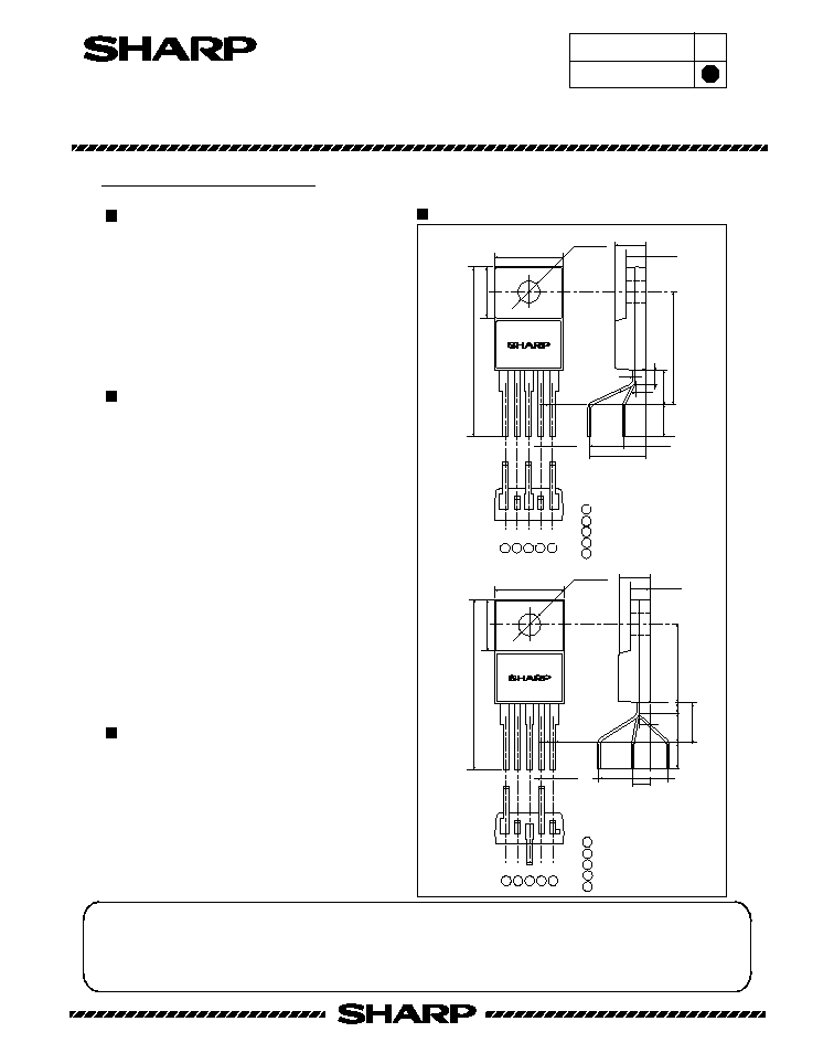
(Unit: mm)
PQ1CG2032FZ
PQ1CG2032RZ
Chopper Regulator
TO-220 Type Chopper Regulator
Tec. PW990302-A
General Description
Outline Dimensions
Features
Applications
Under development
New product
Sharp's chopper regulator
PQ1CG2032FZ/PQ1CG2032RZ
of TO-220 package uses PWM method.
It is suitable for the applications of large voltage difference
between input and output and applications of negative power
supply thanks to its low heat loss.
(1) Maximum switching current: 3.5 A
(2) Built-in ON/OFF control function
(3) Built-in soft start function to suppress overshoot of
output voltage in power on sequeuce or ON/OFF
controll sequence.
(4) Built-in oscillation circuit
(Oscillation frequency : TYP. 70 kHz)
(5) Built-in overheat/overcurrent protection function
(6) TO-220 type package
(7) Variable output voltage
(Output variable range : 1.26 to 35 V/-1.26 to -30 V)
[Possible to choose step-down output/inversing output
according to external connection circuit]
(8)
PQ1CG2032FZ
: Zigzag forming
PQ1CG2032RZ
: Self-stand forming
(1) Switching power supplies
(2) Facsimiles, printers and other OA equipment
(3) Battery chargers
(4) Personal computers and amusement equipment
PQ1CG203
PQ1CG203
10.2 MAX
7.4
±
0.2
(24.6)
(2.0)
16.4
±
0.7
5.0
±
0.5
4.4 MIN
(0.5)
(1.5)
(5.0)
3.2
±
0.5
8.2
±
0.7
4.5
±
0.2
2.8
±
0.2
The dimension in ( ) indicates the
reference dimensions
5-0.8
±
0.1
4-(1.7)
¯3.2
±
0.1
Terminal No.
5
4
3
2
1
10.2 MAX
7.4
±
0.2
(24.6)
The dimension in ( ) indicates the
reference dimensions
5
4
3
2
1
V
I N
V
O U T
C O M
O a d j
O N / O F F
5-0.8
±
0.1
4-(1.7)
¯3.2
±
0.1
Terminal No.
PQ1CG2032FZ
PQ1CG2032RZ
(11.4)
(1.5)
4.7
±
0.6
2.6
±
0.5
4.5
±
0.2
2.8
±
0.2
4.7
±
0.6
(2.2)
6.0
±
0.5
(3.6)
5
4
3
2
1
5
4
3
2
1
V
I N
V
O U T
C O M
O a d j
O N / O F F
75
PQ1CG2032FZ
PQ1CG2032RZ
Chopper Regulator
Tec. PW990302-A
(Ta=25∞C)
(Vin=12 V, Io=0.5 A, Terminal No. 5 open and Ta=25∞C unless otherwise specified)
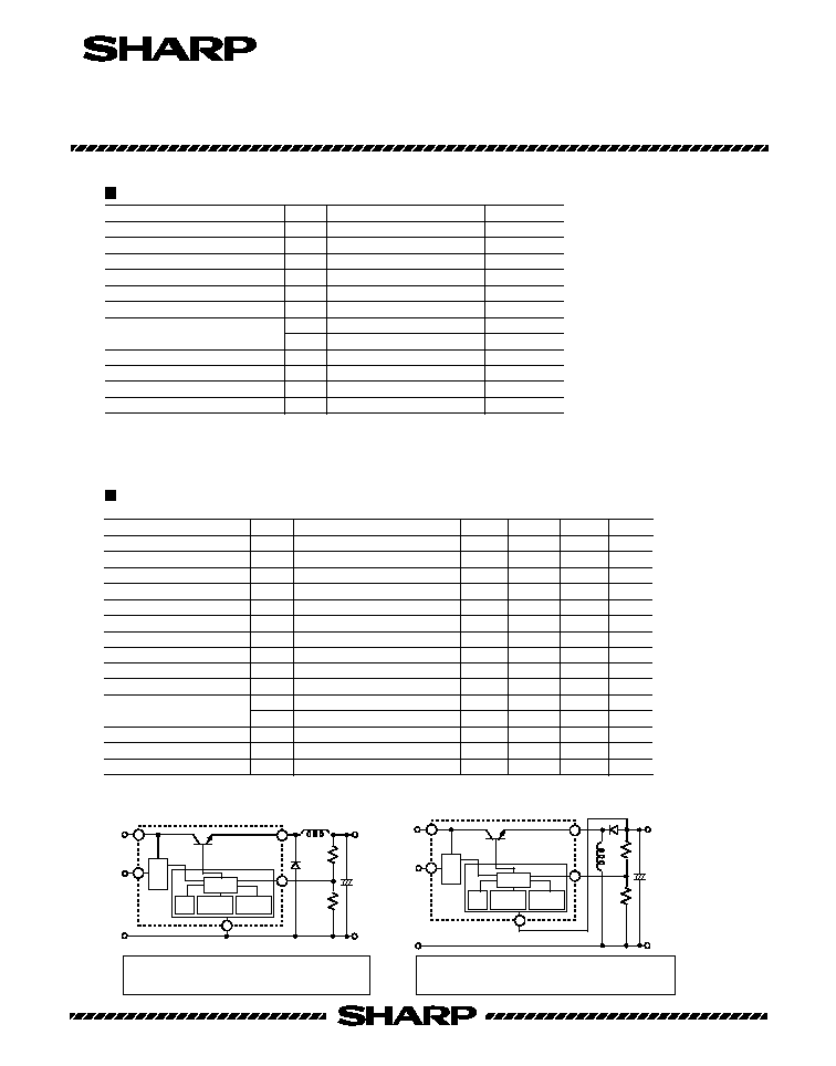
Absolute Maximum Ratings
Electrical Characteristics
Step-down voltage output circuit diagram
Inversing output circuit diagram
*1 Voltage between Vin and COM
*2 Voltage between Vout and COM
*3 Voltage between ON/OFF and COM
*4 P
d1
: No heat sink P
d2
: With infinite heat sink.
*5 Overheat protector may operate for Tj=125 to 150∞C.
As of March 1999
Parameter
Symbol
Conditions
TYP.
MAX.
Unit
Output saturation voltage
Isw
=
3A
1.4
1.8
V
Reference voltage
-
1.26
1.285
V
Reference voltage temperature fluctuation
Tj
=
0 to 125∞C
±
0.5
-
%
Load regulation
Io
=
0.5 to 3A
0.2
1.5
%
Line regulation
Vin
=
8 to 35V
0.5
2.5
%
Efficiency
Io
=
3A
80
-
%
Oscillation frequency
-
70
80
kHz
Oscillation frequency temperature fluctuation
Tj
=
0 to 125∞C
±
2
-
%
Overcurrent detection level
4.2
5.8
A
Charge current
Terminals 2/4 are open, Terminal 5
-
10
-
µ
A
Input threshold voltage
Duty
=
0% Terminal 4
=
0 V, Terminal 5
1.3
-
V
Duty
=
100%, Terminal 4 is open, Terminal 5
2.3
-
V
ON threshold voltage
Terminal 4 = 0 V, Terminal 5
0.8
0.9
V
Standby current
Vin
=
40V,Terminal 5
=
0 V
=
0V
140
400
µ
A
Output OFF-state consumption current
Vin
=
40V,Terminal 5
=
0 V
=
0.9V
MIN.
-
1.235
-
-
-
-
60
-
3.6
-
-
-
0.7
-
-
8
16
mA
-
V
sat
V
ref
V
ref
R
eg
L
R
eg
I
fo
fo
I
L
I
CHG
V
THL
V
THH
V
THON
I
SD
I
QS
Parameter
Symbol
Rating
Unit
*1
Input voltage
40
V
Output adjustment terminal voltage
7
V
Dropout voltage
41
V
*2
Output-COM voltage
-
1
V
*3
ON/OFF control voltage
-
0.3 to 40
V
Switching current
3.5
A
*4
Power dissipation
1.4
W
14
W
*5
Junction temperature
150
∞C
Operating temperature
-
20 to
+
80
∞C
Storage temperature
-
40 to
+
150
∞C
Soldering temperature
260(for 10s)
∞C
V
IN
V
adj
V
I-O
V
out
V
c
I
sw
P
d1
P
d2
T
j
T
opr
T
stg
T
sol
PQ1CG2032FZ/PQ1CG2032RZ
Vo= ≠Vref!(1+R2/R1)
(Vref=1.26V)
Vo= ≠1.26V ~ ≠30V
Here, the upper limit of the absolute value is restricted by 40V-Vi according to the input.
PQ1CG2032FZ/PQ1CG2032RZ
Vo=Vref!(1+R2/R1)
(Vref=1.26V)
Vo=1.26V ~ 35V
Here, the upper limit is restricted by Vin-Vsa value according to the input.
R1
R2
GND
ON/OFF
control
GND
Oscillation
circuit
Overcurrent
protective circuit
Control circuit
Overheat
protective circuit
1
5
3
2
4
ON/OFF
control circuit
Oscillation
circuit
Overcurrent
protective circuit
Control circuit
Overheat
protective circuit
1
R2
R1
ON/OFF
control
GND
2
5
3
4
ON/OFF
control circuit
GND
V
o
V
o
V
IN
V
IN

115
Application Circuits
NOTICE
qThe circuit application examples in this publication are provided to explain representative applications of
SHARP devices and are not intended to guarantee any circuit design or license any intellectual property
rights. SHARP takes no responsibility for any problems related to any intellectual property right of a
third party resulting from the use of SHARP's devices.
qContact SHARP in order to obtain the latest device specification sheets before using any SHARP device.
SHARP reserves the right to make changes in the specifications, characteristics, data, materials,
structure, and other contents described herein at any time without notice in order to improve design or
reliability. Manufacturing locations are also subject to change without notice.
qObserve the following points when using any devices in this publication. SHARP takes no responsibility
for damage caused by improper use of the devices which does not meet the conditions and absolute
maximum ratings to be used specified in the relevant specification sheet nor meet the following
conditions:
(i) The devices in this publication are designed for use in general electronic equipment designs such as:
--- Personal computers
--- Office automation equipment
--- Telecommunication equipment [terminal]
--- Test and measurement equipment
--- Industrial control
--- Audio visual equipment
--- Consumer electronics
(ii)Measures such as fail-safe function and redundant design should be taken to ensure reliability and
safety when SHARP devices are used for or in connection with equipment that requires higher
reliability such as:
--- Transportation control and safety equipment (i.e., aircraft, trains, automobiles, etc.)
--- Traffic signals
--- Gas leakage sensor breakers
--- Alarm equipment
--- Various safety devices, etc.
(iii)SHARP devices shall not be used for or in connection with equipment that requires an extremely
high level of reliability and safety such as:
--- Space applications
--- Telecommunication equipment [trunk lines]
--- Nuclear power control equipment
--- Medical and other life support equipment (e.g., scuba).
qContact a SHARP representative in advance when intending to use SHARP devices for any "specific"
applications other than those recommended by SHARP or when it is unclear which category mentioned
above controls the intended use.
qIf the SHARP devices listed in this publication fall within the scope of strategic products described in the
Foreign Exchange and Foreign Trade Control Law of Japan, it is necessary to obtain approval to export
such SHARP devices.
qThis publication is the proprietary product of SHARP and is copyrighted, with all rights reserved. Under
the copyright laws, no part of this publication may be reproduced or transmitted in any form or by any
means, electronic or mechanical, for any purpose, in whole or in part, without the express written
permission of SHARP. Express written permission is also required before any use of this publication
may be made by a third party.
qContact and consult with a SHARP representative if there are any questions about the contents of this
publication.