(Unit: mm)
Low Power-Loss Voltage Regulator
Tec.PW970702
s
General Description
s
Features
s
Applications
s
Output Voltage Line-up
PQ1S30 series
Low Output Current, Compact Surface Mount Type Low Power-Loss Voltage Regulators
Output voltage
2.2V
PQ1S22
PQ1S23
PQ1S25
PQ1S27
PQ1S28
PQ1S29
PQ1S30
PQ1S31
PQ1S32
PQ1S33
PQ1S47
PQ1S50
2.3V
2.5V
2.7V
2.8V
2.9V
3.0V
3.1V
3.2V
3.3V
4.7V
5.0V
Model No.
Output voltage
Model No.
( ): Typical values
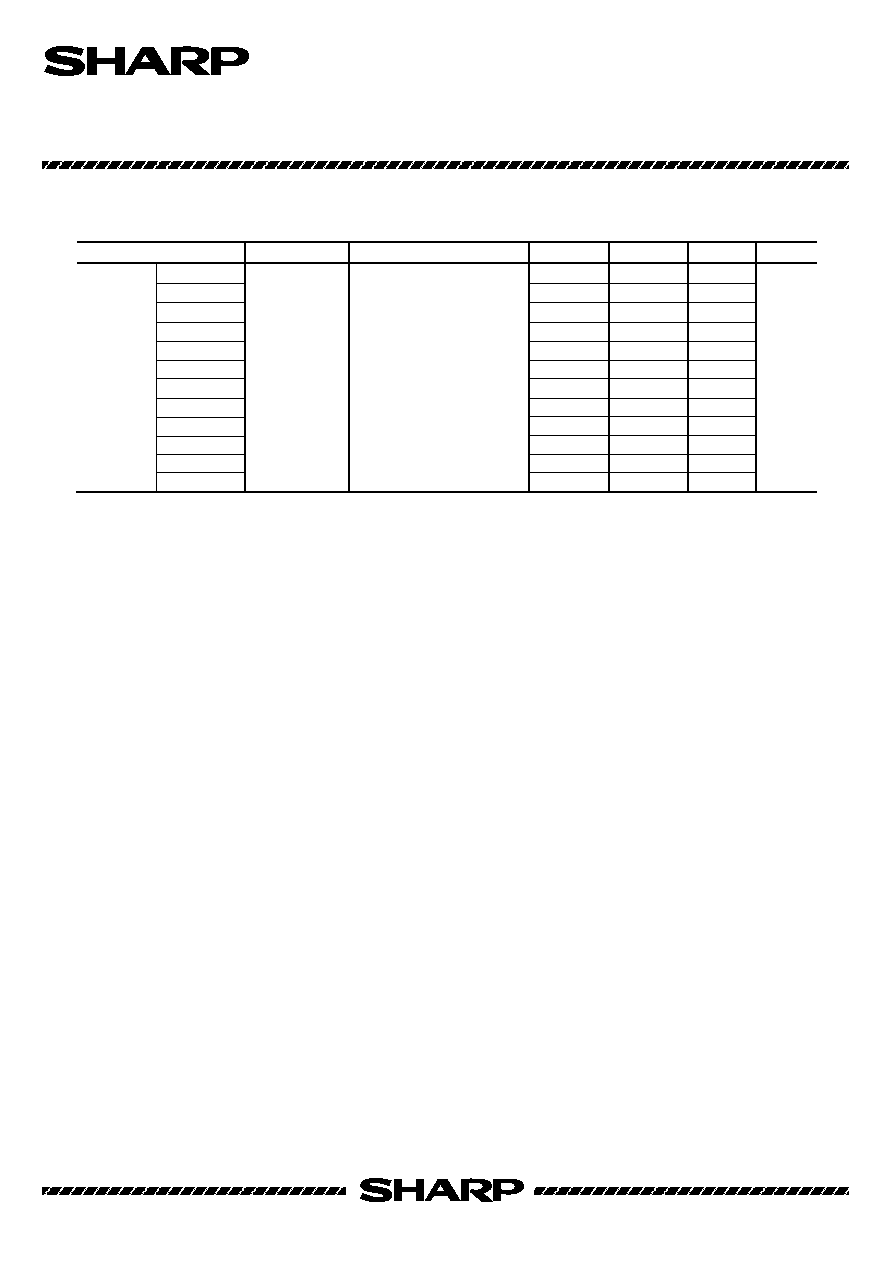
2.2
±
0.2
3.3 to 0.3
15
∞
MAX
1.2
±
0.2
0.15 to 0.1
3.8 MAX
(3.4)
1.4 MAX
0 to 0.1
(0.3)
0.32
±
0.1 x 6
(0.95)
(0.95)
1S30
6
5
4
1
2
3
Internal connection
1 ON/OFF control terminal(Vc)
2 5 GND
3 NC
4 DC output(Vo)
6
DC input(Vin)
Reference
voltage
6
1
2
5
4
Controller
Comparator
Sharp's
PQ1S30 series
are 180mA output, compact resin
mold surface mount package type low power-loss voltage
regulators. They contribute to improve the performance of
analog circuit due to high ripple rejection. They are suitable
for energy and space saving of battery drive compact
equipment such as portable equipment, personal information
tools.
(1) Compact surface mount package(3.4 x 2.2 x 1.2mm)
(2) Low power-loss
(Dropout voltage: TYP.0.1V/MAX. 0.2V at Io=60mA)
(3) High ripple rejection(TYP.60dB)
(4) Low current operation type
(Dissipation current at no load: TYP. 170
µ
A)
(5) Built-in ON/OFF control function
(Dissipation current at OFF-state: MAX. 0.1
µ
A)
(6) Low voltage operation type
(Input voltage: MIN. 1.8V)
(7) Overcurrent, overheat protection functions
(1) Cellular phones
(2) Cordless phones
(3) Personal information tools(PDA)
(4) Cameras/Camcoders
(5) PCMCIA cards for notebook PCs
* It is available for every 0.1V(1.8V to 5.5V)
s
Outline Dimensions
(Notice)
∑ In the absence of device specification sheets, SHARP takes no responsibility for any defects that may occur in equipment using any SHARP devices
shown in catalogs, data books, etc. Contact SHARP in order to obtain the latest device specification sheets before using any SHARP device.
∑ Specifications are subject to change without notice for improvement.
(Internet)
∑ Data for Sharp's optoelectronic/power devices is provided on internet. ( Address http://www.sharp.co.jp/ecg/)

Low Power-Loss Voltage Regulator
Tec.PW970702
s
Absolute Maximum Ratings
PQ1S30 series
(Ta=25∞C)
Parameter
Symbol
Ratings
Unit
*1 Input voltage
Vin
16
V
*1 ON/OFF control terminal voltage
Vc
16
V
Output current
Io
240
mA
*2 Power dissipation
Pd
400
mW
*3 Junction temperature
Tj
150
∞C
Operating temperature
Topr
- 30 to +80
∞C
Storage temperature
Tstg
- 55 to +150
∞C
Soldering temperature
Tsol
260(for 10s)
∞C
*4
(Ta=25∞C)
Parameter
Symbol
Conditions
MIN.
TYP.
MAX.
Unit
Output voltage
Vo
-
150
V
mA
mA
Output current
Io
-
-
-
Recommended output current
-
-
180
240
-
mV
-
80
30
mV
-
mV
Load regulation
RegL1
RegL2
RegL3
Io=5mA to 60mA
Io=5mA to 100mA
Io=5mA to 150mA
Line regulation
RegI
Vi=Vo+1V to Vo+6V
-
5
20
mV
Temperature coefficient of output voltage
TcVo
Io=10mA,Tj= - 25 to 75∞C
10Hz<f<100kHz,
Cn=0.1µF, Io=30mA
-
-
0.05
-
%/∞C
-
30
-
-
50
-
µV
Ripple rejection
RR
Vno
-
60
10
20
90
150
-
dB
Dropout voltage
Output noise
voltage
Vo=3V series
Vo=5V series
Vi-o1
Vi-o2
Io=60mA,*5
Io=150mA,*5
-
0.1
0.2
-
0.29
0.4
V
*6 ON-state voltage for control
Vc(on)
-
1.8
-
-
V
ON-state current for control
Ic(on)
Vc=1.8V
-
12
150
30
µA
OFF-state voltage for control
Vc(off)
-
-
-
-
0.6
V
200
µA
µA
Quiescent current
Iq
Io=0mA
Output OFF-state dissipation current
Iqs
Vin=8V,Vc=0.4V
Response time(Rise time)
Tr
Io=30mA,Vc=0
1.8V, Co=10µF
Noise control terminal voltage
-
-
-
-
0.1
ms
-
0.3
-
V
-
1.25
-
*4 Output current shall be the value when output voltage lowers 0.3V from the voltage at Io=30mA.
*5 Dropout voltage when output voltage lowers 100mV from the voltage at Vin=Vo+1V.
*6 In case of opening control terminal, output voltage turns off.
Refer to the next page.
*1 All are open except GND and applicable terminals.
*2 At surface-mounted condition
*3 Overheat protection may operate at 125<=Tj<=150∞C.
s
Electrical Characteristics