 | –≠–ª–µ–∫—Ç—Ä–æ–Ω–Ω—ã–π –∫–æ–º–ø–æ–Ω–µ–Ω—Ç: PQ30RV2B | –°–∫–∞—á–∞—Ç—å:  PDF PDF  ZIP ZIP |
" In the absence of confirmation by device specification sheets,SHARP takes no responsibility for any defects that may occur in equipment using any SHARP devices
shown in catalogs,data books,etc.Contact SHARP in order to obtain the latest version of the device specification sheets before using any SHARP's device. "
Low Power-Loss Voltage Regulators
PQ30RV1/PQ30RV11/PQ30RV2/PQ30RV21
s
Features
°Compact resin full-mold package
°Low power-loss (Dropout voltage : MAX.0.5V)
°Variable output voltage (setting range : 1.5 to 30V)
s
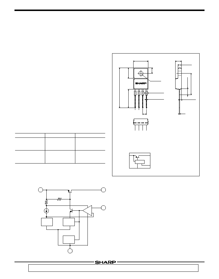
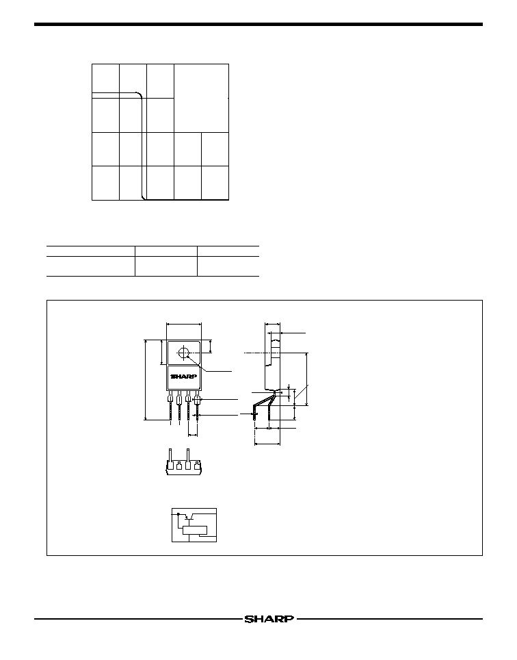
Outline Dimensions
(Unit : mm)
PQ30RV1/PQ30RV11/PQ30RV2/PQ30RV21
Variable Output Low Power-Loss Voltage Regulators
2
3
1
4
PQ30RV11
1 DC input (V
IN
)
2 DC output (V
O
)
3 GND
4 Output voltage
adjustment
terminal (V
ADJ
)
Internal connection diagram
Specific IC
29.1MAX
10.2MAX
7.4±0.2
3.6±0.2
3.2±0.1
+0.3
-0
4-1.4
+0.2
-0.1
4-0.6
13.5MIN
3-(2.54)
4.5±0.2
2.8±0.2
15.6±0.5
4.8MAX
(1.5)
(0.5)
q
1
q
2
q
3
q
4
1
2
4
-
+
3
Reference
voltage
generation
circuit
*ASO
protection
circuit
Overheat
protection
circuit
*ASO:Area of Safety
Operation
s
Equivalent Circuit Diagram
Output voltage
PQ30RV1
PQ30RV11
Reference voltage
precision : ±4%
Reference voltage
precision : ±2%
s
Model Line-ups
1A output
PQ30RV2
PQ30RV21
2A output
s
Applications
°Power supply for print concentration control of electronic
typewriters with display
°Series power supply for motor drives
°Series power supply for VCRs and TVs
Low Power-Loss Voltage Regulators
PQ30RV1/PQ30RV11/PQ30RV2/PQ30RV21
Parameter
Symbol
Rating
Unit
V
IN
V
ADJ
I
O
P
D1
P
D2
T
j
T
opr
T
stg
T
sol
35
7
1
2
1.5
15
18
150
-20 to +80
-40 to +150
260 (For 10s)
V
V
A
W
W
∞C
∞C
∞C
∞C
Input voltage
Output voltage adjustment voltage
Output current
Power dissipation (No heat sink)
Power dissipation
(With infinite heat sink)
Junction temperature
Operating temperature
Storage temperature
Soldering temperature
*1
*1
*2
*1
All are open except GND and applicable terminals.
*2
Overheat protection may operate at T
j
>=125∞C.
s
Absolute Maximum Ratings
(T
a
=25∞C)
PQ30RV1/PQ30RV11
PQ30RV2/PQ30RV21
PQ30RV1/PQ30RV11
PQ30RV2/PQ30RV21
~
V
~
q
3
q
2
q
1
q
4
A
V
V
A
V
IN
I
q
390
I
O
V
O
R
L
0.33
µ
F
47
µ
F
+
V
ref
R
2
R
1
q
3
q
2
q
1
q
4
V
IN
e
i
e
o
390
I
O
R
L
0.33
µ
F
47
µ
F
+
C
ref
R
2
R
1
+
3.3
µ
F
+
I
O
=0.5A
f=120Hz (sine wave)
e
i
=0.5V
rms
RR=20 log (e
i
/e
o
)
V
O
=V
ref
X
1+ --------- =1.25
X
1+ ---------
R
2
R
1
R
2
R
1
[R
1
=390
,V
ref
=1.25V]
Parameter
Symbol
Conditions
V
IN
V
O
R
eg
L
R
eg
I
RR
V
ref
T
c
V
ref
V
i
-
O
I
q
Input voltage
Output voltage
Load regulation
Line regulation
Ripple rejection
Reference voltage
Temperature coefficient of reference voltage
Dropout voltage
Quiescent current
Unit
MAX.
TYP.
MIN.
4.5
1.5
-
-
-
45
55
1.20
1.225
-
-
-
-
R
2
=94
to 8.5k
R
2
=84
to 8.7k
I
O
=5mA to 1A
I
O
=5mA to 2A
V
IN
=11 to 28V
C
ref
=0
Fefer to Fig. 2
C
ref
=3.3µF
-
T
j
=0 to 125∞C
*3
, I
O
=0.5A
*3
, I
O
=2A
I
O
=0
-
-
0.3
0.5
0.5
55
65
1.25
1.25
±1.0
-
-
35
30
1.0
1.0
2.5
-
-
1.30
1.275
-
0.5
7
s
Electrical Characteristics
*3
Input voltage shall be the value when output voltage is 95% in comparison with the initial value.
Unless otherwise specified, condition shall be
V
IN
=15V, V
O
=10V, I
O
=0.5A, R
1
=390
(PQ30RV1/PQ30RV11)
V
IN
=15V, V
O
=10V, I
O
=1.0A, R
1
=390
(PQ30RV2/PQ30RV21)
(T
a
=25∞C)
V
V
%
%
dB
V
%
V
mA
PQ30RV1/PQ30RV2
PQ30RV11/PQ30RV21
PQ30RV1/PQ30RV11
PQ30RV2/PQ30RV21
PQ30RV1/PQ30RV2
PQ30RV11/PQ30RV21
PQ30RV1/PQ30RV11
PQ30RV2/PQ30RV21
Fig.1 Test Circuit
Fig.2 Test Circuit of Ripple Rejection
Low Power-Loss Voltage Regulators
PQ30RV1/PQ30RV11/PQ30RV2/PQ30RV21
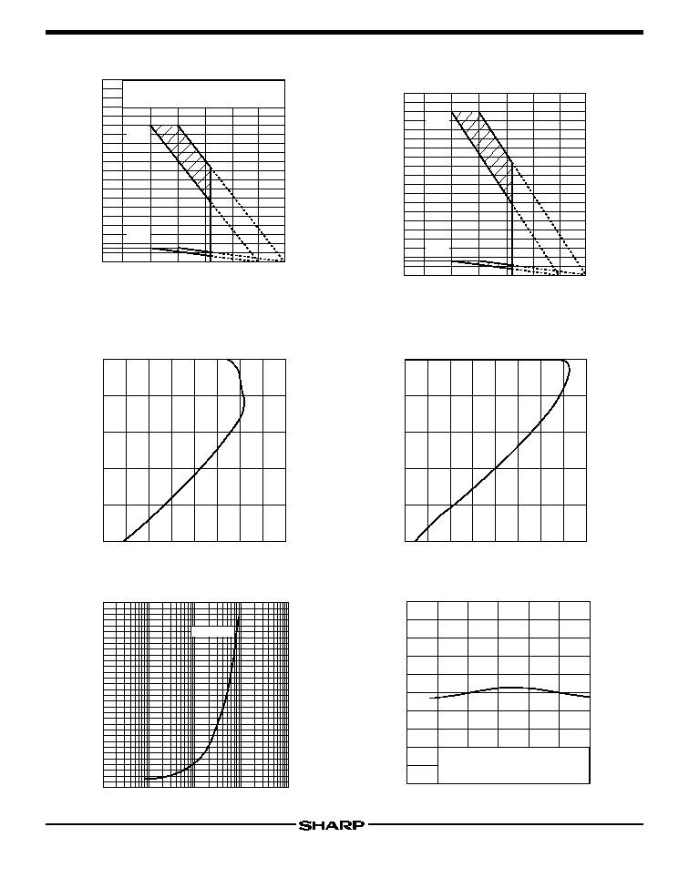
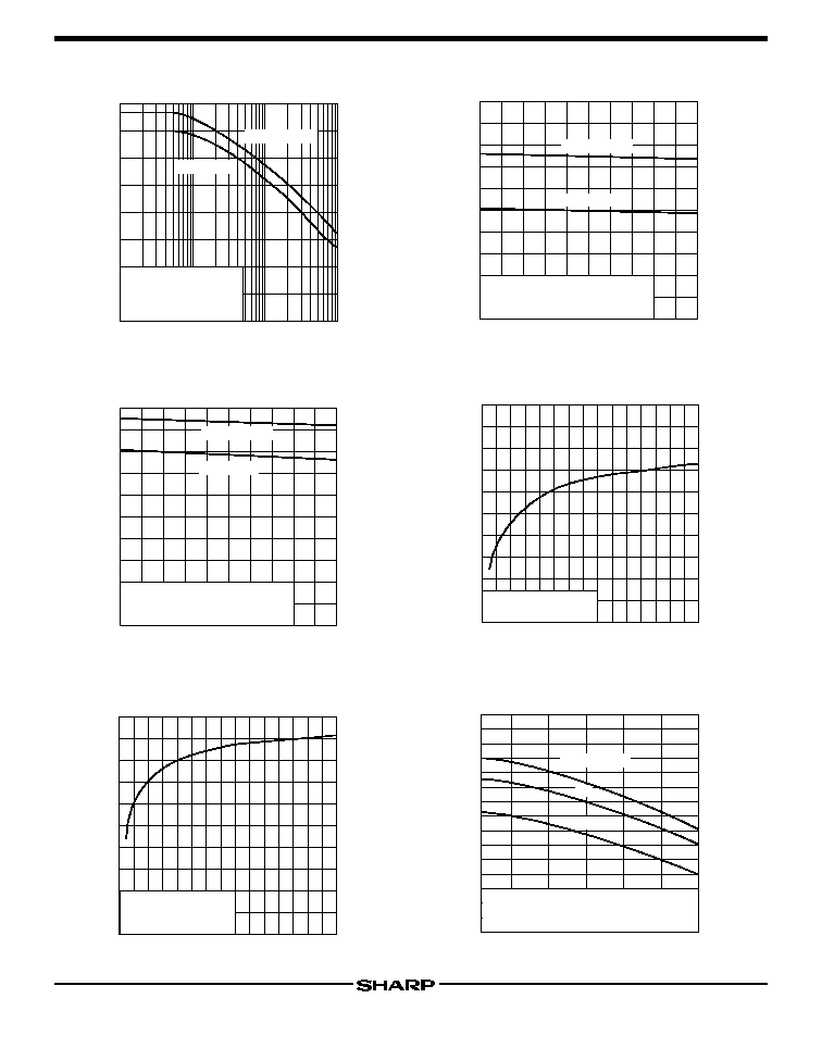
Fig.3 Power Dissipation vs. Ambient
Temperature (PQ30RV1/PQ30RV11)
Fig.4 Power Dissipation vs. Ambient
Temperature (PQ30RV2/PQ30RV21)
Note) Oblique line portion:Overheat protection may operate
in this area.
0
5
10
15
20
0
-20
50
100
150
P
D2
P
D1
Power dissipation P
D
(W)
Ambient temperature T
a
(∞C)
P
D1
:No heat sink
P
D2
:With infinite heat sink
0
5
10
15
20
0
-20
50
100
150
P
D2
P
D1
Power dissipation P
D
(W)
Ambient temperature T
a
(∞C)
P
D1
:No heat sink
P
D2
:With infinite heat sink
Fig.5 Overcurrent Protection Characteristics
(PQ30RV1/PQ30RV11)
Fig.6 Overcurrent Protection Characteristics
(PQ30RV2/PQ30RV21)
0.5
1.0
1.5
2.0
0
0
20
40
60
80
100
Relative output voltage (%)
Output current I
O
(A)
1.0
2.0
3.0
4.0
0
0
20
40
60
80
100
Relative output voltage (%)
Output current I
O
(A)
Fig.7 Output Voltage Adjustment
Characteristics
Fig.8 Reference Voltage Deviation vs.
Junction Temperature
10
1
10
2
10
3
10
4
10
5
R
2
(
)
R
1
390
Output voltage V
O
(V)
0
5
10
15
20
25
30
-25
0
25
50
75
100
125
-10
0
10
Reference voltage deviation
V
ref
(mV)
R
1
=390
,R
2
=2.7k
,V
IN
=15V
I
O
=0.5A(
PQ30RV1/PQ30RV11
)
I
O
= 1A(
PQ30RV2/PQ30RV21
)
Junction temperature T
j
(∞C)
Note) Oblique line portion:Overheat protection may operate
in this area.
Low Power-Loss Voltage Regulators
PQ30RV1/PQ30RV11/PQ30RV2/PQ30RV21
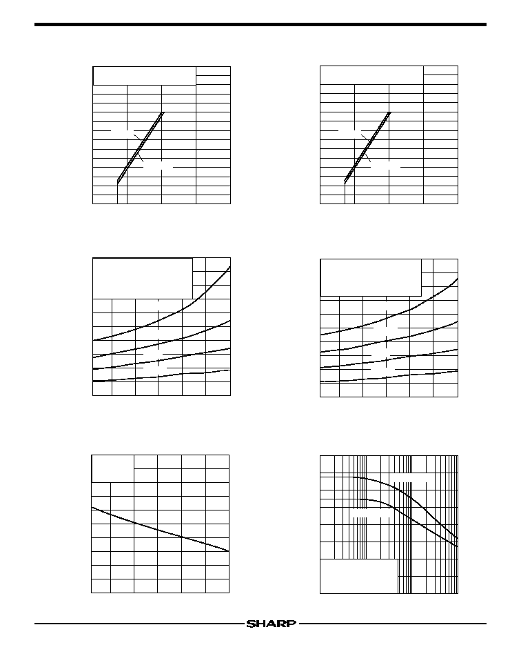
Fig.9 Output Voltage vs. Input Voltage
(PQ30RV1/PQ30RV11)
Fig.11 Dropout Voltage vs. Junction
Temperature (PQ30RV1/PQ30RV11)
Fig.13 Quiescent Current vs. Junction
Temperature
Fig.12 Dropout Voltage vs. Junction
Temperature (PQ30RV2/PQ30RV21)
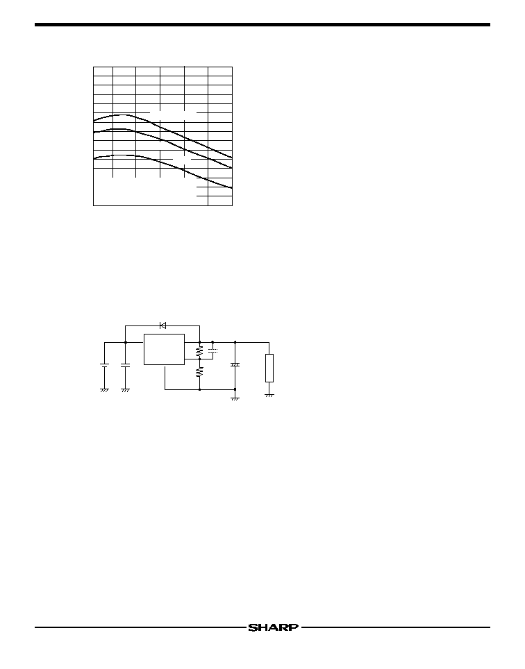
Fig.14 Ripple Rejection vs. Input Ripple
Frequency (PQ30RV1/PQ30RV11)
Fig.10 Output Voltage vs. Input Voltage
(PQ30RV2/PQ30RV21)
0
0
5
10
15
5
10
15
20
R
L
=
R
1
=390
,R
2
=2.7k
,T
j
=25∞C
R
L
=10
Output voltage V
O
(V)
Input voltage V
IN
(V)
0
0
5
10
15
5
10
15
20
R
L
=
R
1
=390
,R
2
=2.7k
,T
j
=25∞C
R
L
=5
Output voltage V
O
(V)
Input voltage V
IN
(V)
-20
0
0
0.1
0.2
0.3
0.4
0.5
25
50
75
100
125
R
1
=390
,R
2
=2.7k
V
IN
:input voltage shall be the
value when output voltage is
95% in comparison with the initial value
Io=1A
0.75A
0.25A
0.5A
Junction temperature T
j
(∞C)
Dropout voltage V
i
-O
(V)
-20
0
0
0.1
0.2
0.3
0.4
0.5
25
50
75
100
125
R
1
=390
,R
2
=2.7k
V
IN
:input voltage shall be the
value when output voltage is
95% in comparison with the initial value
I
O
=2A
1.5A
0.5A
1A
Junction temperature T
j
(∞C)
Dropout voltage V
i
-O
(V)
0
1
2
3
4
5
-20
0
25
50
75
100
125
Quiescent current I
q
(mA)
V
IN
=35V
I
O
=0
Junction temperature T
j
(∞C)
0.1
1
10
100
Input ripple frequency f
(kHz)
Ripple rejection RR (dB)
0
10
20
30
40
50
60
70
80
C
ref
=3.3
µ
F
No C
ref
T
j
=25∞C
R
1
=390
,R
2
=2.7k
I
O
=0.5A,e
i
=0.5V
rms
,
V
IN
=15V
Low Power-Loss Voltage Regulators
PQ30RV1/PQ30RV11/PQ30RV2/PQ30RV21
Fig.15 Ripple Rejection vs. Input Ripple
Frequency (PQ30RV2/PQ30RV21)
Fig.17 Ripple Rejection vs. Output Current
(PQ30RV2/PQ30RV21)
Fig.19 Output Peak Current vs. Input-output
differential voltage (PQ30RV2/PQ30RV21)
Fig.18 Output Peak Current vs. Input-output
differential voltage (PQ30RV1/PQ30RV11)
Fig.20 Output Peak Current vs. Junction
Temperature (PQ30RV1/PQ30RV11)
Fig.16 Ripple Rejection vs. Output Current
(PQ30RV1/PQ30RV11)
0.1
1
10
100
Input ripple frequency f
(kHz)
Ripple rejection RR (dB)
0
10
20
30
40
50
60
70
80
C
ref
=3.3
µ
F
No C
ref
T
j
=25∞C
R
1
=390
,R
2
=2.7k
I
O
=0.5A,e
i
=0.5V
rms
,
V
IN
=15V
0
0.2
0.4
0.6
0.8
1.0
30
50
40
60
70
80
C
ref
=3.3
µ
F
No C
ref
T
j
=25∞C
R
1
=390
,R
2
=2.7k
V
IN
=15V,e
i
=0.5V
rms
,f=120Hz
Output current I
O
(A)
Ripple rejection RR (dB)
0
0.2
0.4
0.6
0.8
1.0
30
50
40
60
70
80
C
ref
=3.3
µ
F
No C
ref
T
j
=25∞C
R
1
=390
,R
2
=2.7k
V
IN
=15V,e
i
=0.5V
rms
,f=120Hz
Output current I
O
(A)
Ripple rejection RR (dB)
0
5
10
15
1.0
1.5
2.0
T
j
=25∞C
R
1
=390
,R
2
=2.7k
Output peak current I
OP
(A)
Input-output differential voltage V
IN
-V
O
(V)
-20
0
25
50
75
100
125
0.5
1.0
1.5
2.0
V
IN
-V
O
=5V
2V
0.5V
R
1
=390
,R
2
=2.7k
I
OP
:Output current when output voltage
is 95% in comparison with the initial value
Junction temperature T
j
(∞C)
Output peak current I
OP
(A)
0
5
10
15
T
j
=25∞C
R
1
=390
,R
2
=2.7k
Output peak current I
OP
(A)
Input-output differential voltage V
IN
-V
O
(V)
3
4
Low Power-Loss Voltage Regulators
PQ30RV1/PQ30RV11/PQ30RV2/PQ30RV21
Fig.21 Output Peak Current vs. Junction
Temperature (PQ30RV2/PQ30RV21)
s
Standard Connection
D
1
: This device is necessary to protect the element from damage when reverse voltage may be applied to the regulator in case of
input short-circuiting.
C
ref
: This device is necessary when it is required to enhance the ripple rejection or to delay the output start-up time(*1).
(*1)Otherwise, it is not necessary.
(Care must be taken since C
ref
may raise the gain, facilitating oscillation.)
(*1)The output start-up time is proportional to C
re f
X
R
2
.
C
IN
, C
O
: Be sure to mount the devices C
IN
and C
O
as close to the device terminal as possible so as to prevent oscillation.
The standard specification of C
IN
and C
O
is 0.33
µ
F and 47
µ
F, respectively. However, ajust them as necessary after checking.
R
1
, R
2
: These devices are necessary to set the output voltage. The output voltage V
O
is given by the following formula:
V
O
=V
ref
X
(1+R
2
/R
1
)
(V
ref
is 1.25V TYP)
The standard value of R
1
is 390
.But value up 10k
does not cause any trouble.
-20
0
25
50
75
100
125
2
3
4
5
V
IN
-V
O
=5V
2V
0.5V
R
1
=390
,R
2
=2.7k
I
OP
:Output current when output voltage
is 95% in comparison with the initial value
Junction temperature T
j
(∞C)
Output peak current I
OP
(A)
q
2
q
3
q
1
q
4
Load
C
ref
390
to10k
R
1
R
2
C
O
+
V
O
D
1
C
IN
V
IN
+
Low Power-Loss Voltage Regulators
PQ30RV1/PQ30RV11/PQ30RV2/PQ30RV21
°ON/OFF operation is available by mounting externally D
2
and R
3
.
°When V
ADJ
is forcibly raised above V
ref
(1.25V TYP) by applying the external signal, the output is turned off (pass transistor of
regulator is turned off). When the output is OFF, V
ADJ
must be higher then V
ref
MAX., and at the same time must be lower than
maximum rating 7V.
In OFF-state, the load current flows to R
L
from V
ADJ
through R
2
. Therefore the value of R
2
must be as high as possible.
°V
O
'
=
V
ADJ
X
R
L
/(R
L
+R
2
)
occurs at the load. OFF-state equivalent circuit R
1
up to 10
is allowed. Select as high value of R
L
and R
2
as possible in this range.
In some case, as output voltage is getting lower (V
O
<1V) , impedance of load resistance rises. In such condition, it is sometime
impossible to obtain the minimum value of V
O
'. So add the dummy resistance indicated by R
D
in the figure to the circuit parallel to
the load.
s
ON/OFF Operation
V
C
High : Output OFF
Low : Output ON
q
2
q
3
q
1
q
4
D
2
R
3
R
1
R
2
C
O
+
V
O
R
L
V
ADJ
D
1
C
IN
V
IN
R
1
Equivalent Circuit
in OFF-state
R
2
R
L
D
2
V
O
'
V
ADJ
R
D
s
An Example of ON/OFF Circuit Using the 1-chip Microcomputer Output Port (PQ30RV1)
<Specification>
Output port of microcomputer
V
OH
(max)
=
0.5 V
V
OH
(min)
=
2.4 V (I
OH
=
0.2mA)
MAX. rating of I
OH
=
0.5mA
Output should be set as follows.
15.6V R
L
=
52
(I
O
=
0.3A)
From V
O
=
1.25V (1+R
2
/R
1
) we get V
O
=
15.6V.
R
2
/R
1
=
11.48
Assuming that V
F
(max)
=
0.8V for D
2
in case of V
OH
(min)
=
2.4V, we get V
ADJ
=
V
OH
(min)-V
F
(max)
=
2.4V-0.8V
=
1.6V. From
V
ref
(max)
=
1.3V we get R
3
=
0
If R
1
=
10k
, we get R
2
=
11.48
X
R
1
=
114.8k
and I
OH
as follows, ingnoring R
L
(52
) :
I
OH
=
1.6V
X
(R
1
+R
2
) /R
1
X
R
2
=
1.6V
X
(10k
+114.8k
) /10k
X
114.8k
=
0.17mA
Hence, I
OH
<0.2mA. Therefore V
OH
(min)is ensured.
Next, assuming that V
F
(min)
=
0.5V for D
2
in case of V
OH
(max), we get:
I
OH
=
(5V-0.5V) (R
1
+R
2
) /R
1
X
R
2
=
0.49mA which is less than the rating.
Figure 1 shows the V
O
-V
C
characteristics when R
1
=
10k
, R
2
=
115k
, R
3
=
0
, V
IN
=
17V, R
L
=
52
, and D
1
=
1S2076A (Hitachi).
Low Power-Loss Voltage Regulators
PQ30RV1/PQ30RV11/PQ30RV2/PQ30RV21
s
Outline Dimensions (PQ30RV1B/PQ30RV2B)
(Unit : mm)
Output Voltage vs. Control Voltage (PQ30RV1)
PQ30RV1B
Output voltage
precision:±2.5%
s
Model Line-ups for Lead Forming Type
5V output
Output voltage
PQ30RV2B
2A output
0
1
2
3
4
5
5
10
15
Control voltage V
C
(V)
V
IN
=17V
R
L
=52
R
1
=10k
R
2
=115k
R
3
=0
D
1
=1S2076A
Output voltage V
O
(V)
PQ30RV11
2
3
1
4
1 DC input (V
IN
)
2 DC output (V
O
)
3 GND
4 Output voltage
minute
adjustment
terminal (V
ADJ
)
Specific IC
Internal connection diagram
(24.6)
10.2MAX
7.4±0.2
3.6±0.2
3.2±0.1
+0.3
-0
4-1.4
+0.2
-0.1
4-0.6
3-(2.54)
4.5±0.2
2.8±0.2
16.4±0.7
(2.0)
(3.2)
q
1
q
2
q
3
q
4
(5±0.5)
5±0.5
8.2±0.7
(0.5)
(1.5)
4.4MIN
∑ ( ) : Typical value
∑ Radius of lead forming portion:R=0.5 to 1.5mm
Note) The value of absolute maximum ratings and electrical characteristics is same as ones of
PQ30RV11/21 series.

115
Application Circuits
NOTICE
qThe circuit application examples in this publication are provided to explain representative applications of
SHARP devices and are not intended to guarantee any circuit design or license any intellectual property
rights. SHARP takes no responsibility for any problems related to any intellectual property right of a
third party resulting from the use of SHARP's devices.
qContact SHARP in order to obtain the latest device specification sheets before using any SHARP device.
SHARP reserves the right to make changes in the specifications, characteristics, data, materials,
structure, and other contents described herein at any time without notice in order to improve design or
reliability. Manufacturing locations are also subject to change without notice.
qObserve the following points when using any devices in this publication. SHARP takes no responsibility
for damage caused by improper use of the devices which does not meet the conditions and absolute
maximum ratings to be used specified in the relevant specification sheet nor meet the following
conditions:
(i) The devices in this publication are designed for use in general electronic equipment designs such as:
--- Personal computers
--- Office automation equipment
--- Telecommunication equipment [terminal]
--- Test and measurement equipment
--- Industrial control
--- Audio visual equipment
--- Consumer electronics
(ii)Measures such as fail-safe function and redundant design should be taken to ensure reliability and
safety when SHARP devices are used for or in connection with equipment that requires higher
reliability such as:
--- Transportation control and safety equipment (i.e., aircraft, trains, automobiles, etc.)
--- Traffic signals
--- Gas leakage sensor breakers
--- Alarm equipment
--- Various safety devices, etc.
(iii)SHARP devices shall not be used for or in connection with equipment that requires an extremely
high level of reliability and safety such as:
--- Space applications
--- Telecommunication equipment [trunk lines]
--- Nuclear power control equipment
--- Medical and other life support equipment (e.g., scuba).
qContact a SHARP representative in advance when intending to use SHARP devices for any "specific"
applications other than those recommended by SHARP or when it is unclear which category mentioned
above controls the intended use.
qIf the SHARP devices listed in this publication fall within the scope of strategic products described in the
Foreign Exchange and Foreign Trade Control Law of Japan, it is necessary to obtain approval to export
such SHARP devices.
qThis publication is the proprietary product of SHARP and is copyrighted, with all rights reserved. Under
the copyright laws, no part of this publication may be reproduced or transmitted in any form or by any
means, electronic or mechanical, for any purpose, in whole or in part, without the express written
permission of SHARP. Express written permission is also required before any use of this publication
may be made by a third party.
qContact and consult with a SHARP representative if there are any questions about the contents of this
publication.