 | –≠–ª–µ–∫—Ç—Ä–æ–Ω–Ω—ã–π –∫–æ–º–ø–æ–Ω–µ–Ω—Ç: PQ30VB11 | –°–∫–∞—á–∞—Ç—å:  PDF PDF  ZIP ZIP |
" In the absence of confirmation by device specification sheets,SHARP takes no responsibility for any defects that may occur in equipment using any SHARP devices
shown in catalogs,data books,etc.Contact SHARP in order to obtain the latest version of the device specification sheets before using any SHARP's device. "
Low Power-Loss Voltage Regulators
PQ30VB11
s
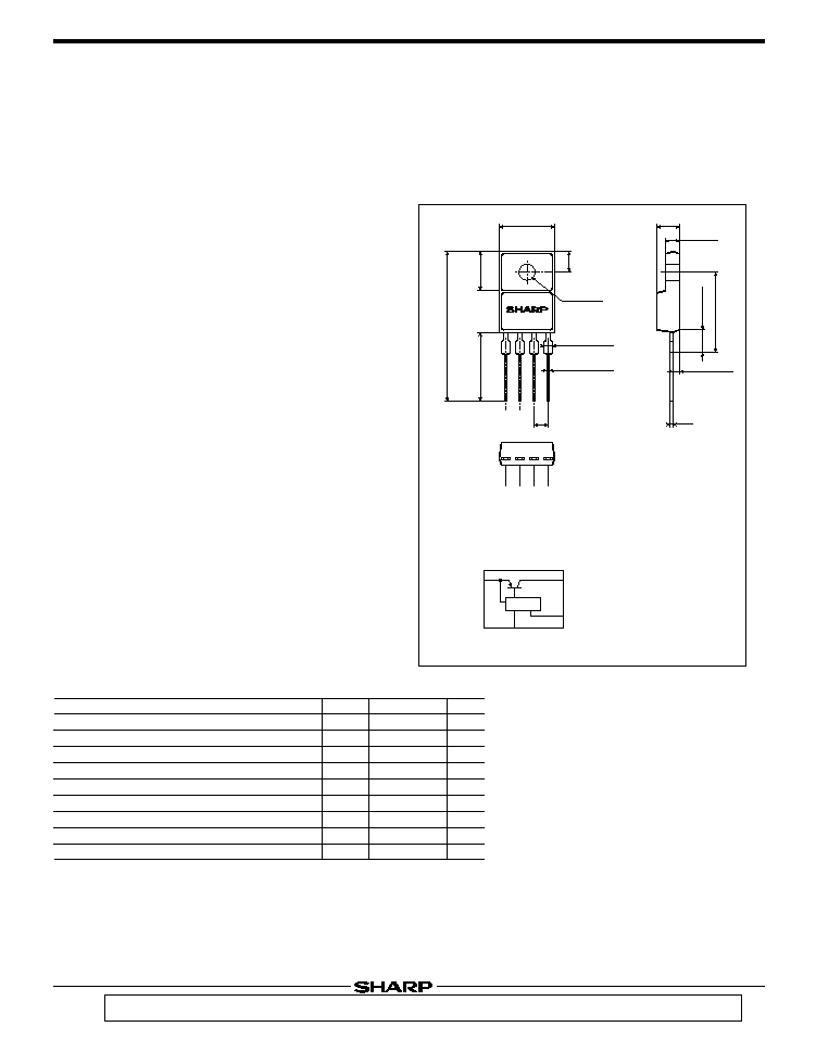
Outline Dimensions
(Unit : mm)
PQ30VB11
Variable Output Low Power-Loss Voltage Regulator(Built-in Overheat Shut-Down Function)
s
Features
°Compact resin full-mold package
°Low power-loss (Dropout voltage : MAX. 0.5V)
°Overheat shut-down function (keep shut-down output until
power-on again)
°Variable output voltage (Setting range : 1.5 to 30V)
°Overcurrent protection type
°High-precision output type (Reference voltage precision :
±
2.0%)
s
Applications
°Series power supply for TVs and VCRs
°Switching power supply
Parameter
Symbol
Rating
Unit
V
IN
V
ADJ
I
O
P
D1
P
D2
T
j
T
opr
T
atg
T
sol
35
7
1
1.25
12.5
150
-20 to +80
-40 to +150
260
V
V
A
W
W
∞C
∞C
∞C
∞C
Input voltage
Output adjustment terminal voltage
Output current
Power dissipation (No heat sink)
Power dissipation (With infinite heat sink)
Junction temperature
Operating temperature
Storage temperature
Soldering temperature
*1
*1
*2
*3
*1
All are open except GND and applicable terminals.
*2
Overheat shut-down function operates at T
j
>=110∞C.
*3
For 10s
s
Absolute Maximum Ratings
(T
a
=25∞C)
2
3
1
4
PQ30VB11
1 DC input (V
IN
)
2 DC output (V
O
)
3 GND
4 Output voltage
minute
adjustment
terminal (V
ADJ
)
Internal connection diagram
Specific IC
29.1MAX
10.2MAX
7.4±0.2
3.6±0.2
3.2±0.1
+0.3
-0
4-1.4
+0.2
-0.1
4-0.6
13.5MIN
3-(2.54)
4.5±0.2
2.8±0.2
15.6±0.5
4.8MAX
(1.5)
(0.5)
q
1
q
2
q
3
q
4
∑ Please refer to the chapter" Handling Precautions ".
PQ30VB11
Low Power-Loss Voltage Regulators
Parameter
Symbol
Conditions
V
IN
V
O
R
eg
L
R
eg
I
RR
V
ref
T
e
V
ref
V
i
-
O
I
q
T
sd
Input voltage
Output voltage
Load regulation
Line regulation
Ripple rejection
Reference voltage
Temperature coefficient of reference voltage
Dropout voltage
Quiescent current
Overheat shut-down temperature
Unit
MAX.
TYP.
MIN.
4.5
1.5
-
-
45
1.225
-
-
-
110
-
-
I
O
=5mA
to
1A
V
IN
=11 to 28V
Refer to Fig. 2
T
j
=0 to 125∞C, I
O
=5mA
*4
, I
O
=0.5A
I
O
=0
-
-
0.3
0.5
55
1.25
±1.0
-
-
130
35
30
1.0
2.5
-
1.275
-
0.5
7
150
s
Electrical Characteristics
*4
Input voltage shall be the value when output voltage is 95% in comparison with the initial value.
(Unless otherwise specified, condition shall be V
IN
=15V, Vo=10V, Io=0.5A, R
1
=390
, T
a
=25∞C)
V
V
%
%
dB
V
%
V
mA
∞C
Fig.1 Test Circuit
Fig.2 Test Circuit of Ripple Rejection
~
V
~
q
3
q
2
q
1
q
4
A
V
V
A
V
IN
I
q
390
I
O
V
O
R
L
0.33
µ
F
47
µ
F
+
V
ref
R
2
R
1
q
3
q
2
q
1
q
4
V
IN
e
i
e
o
390
I
O
R
L
0.33
µ
F
47
µ
F
+
R
2
R
1
+
I
O
=0.5A
f=120Hz (sine wave)
e
i
=0.5V
rms
RR=20 log (e
i
/e
o
)
V
O
=V
ref
X
1+ ----------- =1.25
X
1+ -----------
R
2
R
1
R
2
R
1
[R
1
=390
,V
ref
=1.25V]
0.5
1.0
1.5
2.0
0
20
40
60
80
100
Relative output voltage (%)
Output current I
O
(A)
Fig.4 Overcurrent Protection
Characteristics (Typical Value)
Fig.3 Power Dissipation vs. Ambient
Temperature
-20
0
0
1
2
3
4
5
6
7
8
9
10
11
12
13
50
100
150
P
D2
P
D1
Power dissipation P
D
(W)
Ambient temperature T
a
(∞C)
P
D1
:No heat sink
P
D2
:With infinite heat sink
Note) Oblique line portion:Overheat protection operates in this
area.
Low Power-Loss Voltage Regulators
PQ30VB11
Fig.5 Output Voltage Adjustment
Characteristics
Fig.7 Dropout Voltage vs. Junction
Temperature
Fig.9 Output Peak Current vs. Junction
Temperature
Fig.8 Circuit Operating Current vs. Input
Voltage
Fig.6 Output Voltage vs. Input Voltage
0.01
0.1
1
10
R
2
(k
)
R
1
=390
0
5
10
15
20
25
30
Output voltage V
O
(V)
1
2
3
4 5
6
7
8 9 10 11 12
R
L
=
R
L
=20
R
L
=10
0
1
2
3
4
5
6
7
8
9
10
T
j
=25∞C
V
O
=10V
R
1
=390
R
2
=2710
Output voltage V
O
(V)
Input voltage V
IN
(V)
-25
25
50
75
100
125
0
I
O
=1A
0.75A
0.5A
0.25A
Junction temperature T
j
(∞C)
Dropout voltage V
i
-O
(V)
0
0.05
0.1
0.2
0.25
0.3
0.35
0.4
0.5
0.45
0.15
1 2 3 4 5 6 7 8 9 10 11 12 13 14 15
R
L
=
R
L
=10
R
L
=20
0
5
10
15
20
25
30
35
40
T
j
=25∞C
V
O
=10V
R
1
=390
R
2
=2710
Input voltage V
IN
(V)
Circuit operating current I
BIAS
(mA)
-25
25
50
75
100
125
0
1.2
1.4
1.6
1.8
2
2.2
V
IN
-V
O
=5V
2V
1V
0.5V
Junction temperature T
j
(∞C)
Output peak current I
OP
(A)
I
OP
:Output current when output voltage
is 95% in comparison with the initial value
PQ30VB11
Low Power-Loss Voltage Regulators
s
Overheat Shut-down Characteristics
s
ON/OFF Operation
V
O
T
j
OFF
ON
V
IN
*Tsd
* Tsd:Overheat shut-down temperature (T
j
>=110∞C)
1 Overheat shut-down operates at T
j=
Tsd and output OFF-state is maintained.
2 OFF-state is kept until V
IN
is once turned off.
V
C
High : Output OFF
Low : Output ON
q
2
q
3
q
1
q
4
D
2
R
3
R
1
R
2
C
O
+
V
O
R
L
V
ADJ
D
1
C
IN
V
IN
R
1
Equivalent Circuit
in OFF-state
R
2
R
L
D
2
V
O
'
V
ADJ
R
D
°ON/OFF operation is available by mounting externally D
2
and R
3
.
°When V
ADJ
is forcibly raised above V
ref
(1.25V TYP) by applying the external signal, the output is turned off(pass transistor of
regulator is turned off). When the output is OFF, V
ADJ
must be higher then V
ref
MAX., and at the same time must be lower than
maximum rating 7V.
In OFF-state, the load current flows to R
L
from V
ADJ
through R
2
. Therefore the value of R
2
must be as high as possible.
°V
O
'=V
ADJ
X
R
L
/ (R
L
+R
2
)
occurs at the load. OFF-state equivalent circuit R
1
up to 10k
is allowed. Select as high value of R
L
and R
2
as possible in this range.
In some case, as output voltage is getting lower (V
O
<1V), impedance of load resistance rises. In such condition, it is sometime
impossible to obtain the minimum value of V
O
'.So add the dummy resistance indicated by R
D
in the figure to the circuit parallel to the
load.