 | –≠–ª–µ–∫—Ç—Ä–æ–Ω–Ω—ã–π –∫–æ–º–ø–æ–Ω–µ–Ω—Ç: PQ3RF33 | –°–∫–∞—á–∞—Ç—å:  PDF PDF  ZIP ZIP |
" In the absence of confirmation by device specification sheets,SHARP takes no responsibility for any defects that may occur in equipment using any SHARP devices
shown in catalogs,data books,etc.Contact SHARP in order to obtain the latest version of the device specification sheets before using any SHARP's device. "
Low Power-Loss Voltage Regulators
PQ3RF23/PQ3RF33
s
Features
°3.3V output
°High output current
2A type :
PQ3RF23
3.5A type :
PQ3RF33
°Compact resin full-mold package (TO-220 package)
°Low power-loss (Dropout voltage : MAX. 0.5V)
°High-precision output voltage type
Output voltage precision :
±
2.5%
°Built-in ON/OFF control function
°Built-in overcurrent protection, overheat protection function
s
Applications
°Power supplies for various electronic equipment such as
personal computers
s
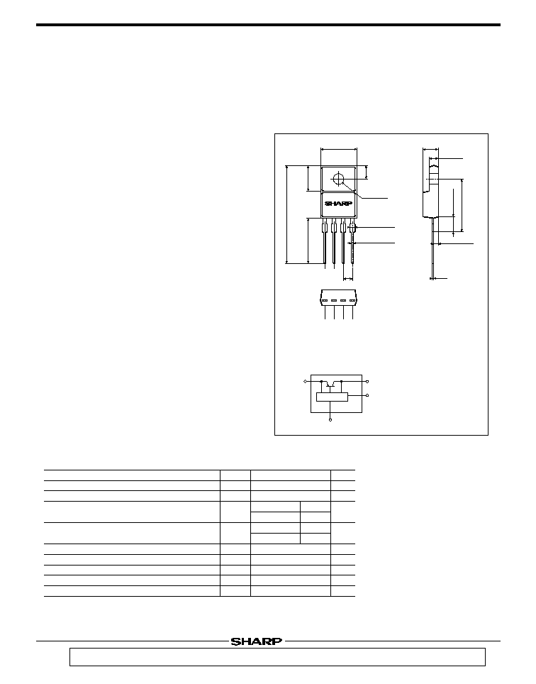
Outline Dimensions
PQ3RF23/PQ3RF33
(Unit : mm)
3.3V Output, High Output Current (2A, 3.5A) Type Low Power-loss Voltage Regulators
Parameter
Symbol
Rating
Unit
V
IN
V
C
I
O
P
D1
P
D2
T
j
T
opr
T
stg
T
sol
10
10
18
150
-20 to +80
-40 to +150
260(For 10s.)
V
V
A
W
W
∞C
∞C
∞C
∞C
Input voltage
ON/OFF control terminal voltage
Output current
Power dissipation (No heat sink)
Power dissipation (With infinite heat sink)
Junction temperature
Operating temperature
Storage temperature
Soldering temperature
*1
*1
*2
*1
All are open except GND and applicable terminals.
*2
Overheat protection may operate at 125=<T
j
=<150∞C.
s
Absolute Maximum Ratings
2
3.5
1.5
1.8
PQ3RF23
PQ3RF33
PQ3RF23
PQ3RF33
(T
a
=25∞C)
PQ3RF23
2
3
1
4
29.1MAX
10.2MAX
7.4±0.2
3.6±0.2
3.2±0.1
+0.3
-0
4-1.4
+0.2
-0.1
4-0.6
13.5MIN
3-(2.54)
4.5±0.2
2.8±0.2
15.6±0.5
4.8MAX
(1.5)
(0.5)
q
1
q
2
q
3
q
4
1 DC input (V
IN
)
2 DC output (V
O
)
3 GND
4 ON/OFF control
terminal (V
C
)
Control circuit
Internal connection diagram
∑ Please refer to the chapter" Handling Precautions ".
Low Power-Loss Voltage Regulators
,,,
,,,
,,,
,,,
20
0
5
1.5
10
15
18
-20
0
20
40
60
80
P
D2
P
D1
Power dissipation P
D
(W)
Ambient temperature T
a
(∞C)
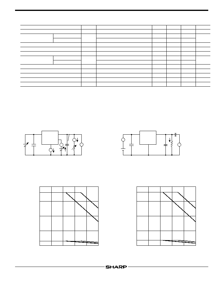
Fig.1 Test Circuit
Parameter
Symbol
Conditions
Output voltage
Load regulation
Line regulation
Temperature coefficient of output voltage
Ripple rejection
Dropout voltage
ON-state voltage for control
ON-state current for control
OFF-state voltage for control
OFF-state current for control
Quiescent current
Unit
MAX.
TYP.
MIN.
3.218
-
-
-
-
45
-
-
2
-
-
-
-
3.3
0.2
0.2
0.5
±0.02
55
-
-
-
-
-
-
-
3.382
2
2
2.5
-
-
0.5
0.5
-
20
0.8
-0.4
10
s
Electrical Characteristics
*3
Input voltage shall be the value when output voltage is 95% in comparison with the initial value.
*4
In case of opening control terminal 4,output voltage turns on.
(Unless otherwise specified,conditions shall be I
O
=1.0A[
PQ3RF23
]/I
O
=1.5A[
PQ3RF33
],V
IN
=5V,T
a
=25∞C)
PQ3RF23
PQ3RF33
PQ3RF23
PQ3RF33
V
O
R
eg
L
R
eg
I
T
C
V
O
RR
V
i
-
O
V
C(ON)
I
C(ON)
V
C(OFF)
I
C(OFF)
I
q
-
I
O
=5mA to 2.0A
I
O
=5mA to 3.5A
V
IN
=4 to 10V
T
j
=0 to 125∞C
-
*3
, I
O
=2.0A
*3
, I
O
=3.0A
-
V
C
=2.7V
-
V
C
=0.4V
I
O
=0A
V
%
%
%/∞C
dB
V
V
µ
A
V
mA
mA
*4
Fig.2 Test Circuit of Ripple Rejection
q
3
q
2
q
1
q
4
A
V
A
A
V
IN
I
q
I
C
I
O
V
O
V
C
R
L
0.33
µ
F
47
µ
F
+
Fig.4
Power dissipation vs. Ambient
temperature (PQ3RF33)
Fig.3
Power Dissipation vs. Ambient
Temperature (PQ3RF23)
,,,
,,,
,,,
,,,
20
0
5
1.8
10
15
18
-20
0
20
40
60
80
P
D2
P
D1
Power dissipation P
D
(W)
Ambient temperature T
a
(∞C)
Note) Oblique line portion:Overheat protection may operate
in this area.
q
3
q
2
q
1
q
4
V
e
i
V
IN
I
O
e
o
R
L
0.33
µ
F
47
µ
F
+
+
~
~
f=120Hz (sine wave)
e
i
=0.5V
rms
V
IN
=5V
I
O
=0.5A
RR=20 log (e
i
/e
o
)
Note) Oblique line portion:Overheat protection may operate
in this area.
PQ3RF23/PQ3RF33
Low Power-Loss Voltage Regulators
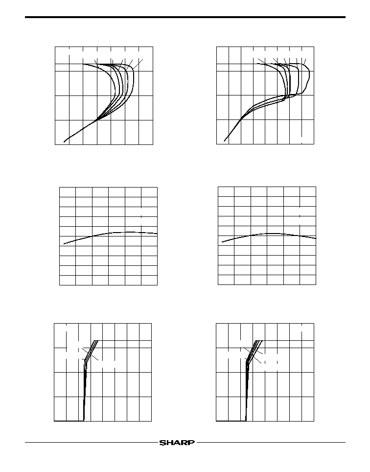
-25
0
25
50
75
100
125
Junction temperature T
j
(∞C)
-100
-80
-60
-40
-20
20
40
60
80
0
100
Output voltage deviation
V
O
(mV)
V
IN
=5V
I
O
=0A
5
0
3
4
6
7
2
1
8
2
3
1
4
Input voltage V
IN
(V)
Output voltage V
O
(V)
T
j
=25∞C
R
L
=0.94
R
L
=1.65
R
L
=3.3
R
L
=
5
0
3
4
6
7
2
1
8
2
3
1
4
Input voltage V
IN
(V)
Output voltage V
O
(V)
T
j
=25∞C
R
L
=1.65
R
L
=3.3
R
L
=
Output voltage deviation
V
O
(mV)
Junction temperature T
j
(∞C)
-25
0
25
50
75
100
125
-100
-80
-60
-40
-20
20
40
60
80
0
100
V
IN
=5V
I
O
=0A
PQ3RF23/PQ3RF33
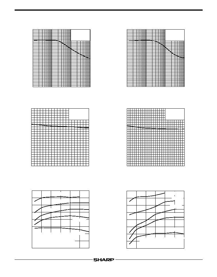
Fig.7
Output Voltage Deviation vs.
Junction Temperature
Fig.9
Output Voltage vs. Input Voltage
Fig.8
Output Voltage Deviation vs.
Junction Temperature
Fig.10 Output Voltage vs. Input Voltage
(PQ3RF23)
(PQ3RF33)
(PQ3RF33)
(PQ3RF23)
Output voltage V
O
(V)
Output current I
O
(A)
5
0
3
4
6
7
8
2
1
2
3
1
4
T
j
=25∞C
V
IN
=3.8V 4.3V 5V 7V 10V
Fig.5
Overcurrent Protection Characteristics
Fig.6
Overcurrent Protection Characteristics
(PQ3RF33)
(PQ3RF23)
Output voltage V
O
(V)
Output current I
O
(A)
5
0
3
4
6
7
2
1
2
3
1
4
T
j
=25∞C
V
IN
=3.8V 4.3V 5V 7V 10V
Low Power-Loss Voltage Regulators
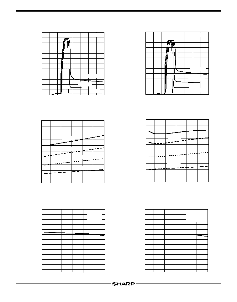
-25
0
0
0.1
0.2
0.3
0.4
0.5
25
50
75
100
125
I
O
=3.5A
I
O
=3.0A
I
O
=1.0A
I
O
=2.0A
Junction temperature T
j
(∞C)
Dropout voltage V
i
-O
(V)
-25
0
0
0.1
0.2
0.3
0.4
0.5
25
50
75
100
125
I
O
=2.0A
I
O
=1.5A
I
O
=0.5A
I
O
=1.0A
Junction temperature T
j
(∞C)
Dropout voltage V
i
-O
(V)
1
2
3
4
5
6
7
8
R
L
=
R
L
=0.94
R
L
=1.65
R
L
=3.3
0
50
100
T
j
=25∞C
Input voltage V
IN
(V)
Circuit operating current I
BIAS
(mA)
1
2
3
4
5
6
7
8
R
L
=
R
L
=1.65
R
L
=3.3
0
50
100
T
j
=25∞C
Input voltage V
IN
(V)
Circuit operating current I
BIAS
(mA)
Fig.11 Circuit Operating Current vs. Input
Voltage
Fig.13 Dropout Voltage vs. Junction
Temperature
Fig.12 Circuit Operating Current vs. Input
Voltage
Fig.14 Dropout Voltage vs. Junction
Temperature
(PQ3RF23)
(PQ3RF33)
(PQ3RF23)
(PQ3RF33)
PQ3RF23/PQ3RF33
0
1
2
3
4
5
-25
0
25
50
75
100
125
V
IN
=5V
I
O
=0A
Junction temperature T
j
(∞C)
Quiescent current I
q
(mA)
0
1
2
3
4
5
-25
0
25
50
75
100
125
V
IN
=5V
I
O
=0A
Junction temperature T
j
(∞C)
Quiescent current I
q
(mA)
Fig.15 Quiescent Current vs. Junction
Temperature
Fig.16 Quiescent Current vs. Junction
Temperature
(PQ3RF23)
(PQ3RF33)
Low Power-Loss Voltage Regulators
Ripple rejection RR (dB)
80
0
0.5
1
1.5
2
Output current I
O
(A)
40
50
60
70
e
i
=0.5V
rms
f=120Hz
V
IN
=5V
1
80
0
3
2.5
2
1.5
0.5
30
40
50
60
70
e
i
=0.5V
rms
f=120Hz
V
IN
=5V
Output current I
O
(A)
Ripple rejection RR (dB)
0.1
1
10
100
Input ripple frequency f
(kHz)
Ripple rejection RR (dB)
0
10
20
30
40
50
60
70
80
e
i
=0.5V
rms
I
O
=0.5A
V
IN
=5V
0.1
1
10
100
Input ripple frequency f
(kHz)
Ripple rejection RR (dB)
0
10
20
30
40
50
60
70
80
e
i
=0.5V
rms
I
O
=0.5A
V
IN
=5V
Fig.17 Ripple Rejection vs. Input Ripple
Frequency
Fig.19 Ripple Rejection vs. Output Current
Fig.18 Ripple Rejection vs. Input Ripple
Frequency
Fig.20 Ripple Rejection vs. Output Current
PQ3RF23/PQ3RF33
(PQ3RF23)
(PQ3RF33)
(PQ3RF23)
(PQ3RF33)
Junction temperature T
j
(∞C)
Output peak current I
OP
(A)
I
OP
:Output current when
output voltage is 95%
in comparison with
the initial value
-25
0
2.0
6.0
5.5
5.0
4.5
4.0
3.5
3.0
2.5
25
50
75
100
125
V
IN
=10V
V
IN
=7V
V
IN
=4.3V
V
IN
=3.8V
V
IN
=5V
-25
0
4.0
8.0
7.5
7.0
6.5
6.0
5.5
5.0
4.5
25
50
75
100
125
V
IN
=10V
V
IN
=7V
V
IN
=4.3V
V
IN
=3.8V
V
IN
=5V
I
OP
:Output current when
output voltage is 95% in
comparison with the initial value
Junction temperature T
j
(∞C)
Output peak current I
OP
(A)
Fig.21 Output Peak Current vs. Junction
Temperature
Fig.22 Output Peak Current vs. Junction
Temperature
(PQ3RF33)
(PQ3RF23)
Low Power-Loss Voltage Regulators
PQ3RF23/PQ3RF33
s
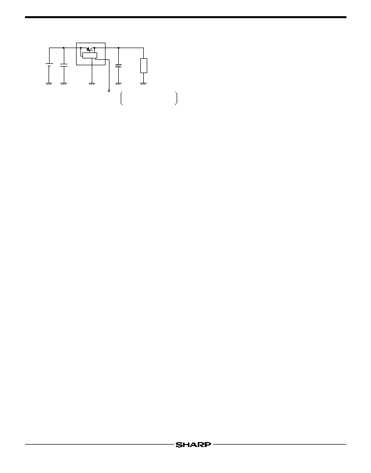
Typical Application
Specific IC
q
2
q
3
q
1
q
4
V
O
0.33
µ
F
C
O
DC input
+
Load
High or Open :output ON
Low :output OFF
ON/OFF Control