 | –≠–ª–µ–∫—Ç—Ä–æ–Ω–Ω—ã–π –∫–æ–º–ø–æ–Ω–µ–Ω—Ç: PQ5EV5 | –°–∫–∞—á–∞—Ç—å:  PDF PDF  ZIP ZIP |
PQ5EV3/PQ5EV5/
PQ5EV7
PQ5EV3/PQ5EV5/PQ5EV7
s
Absolute Maximum Ratings
s
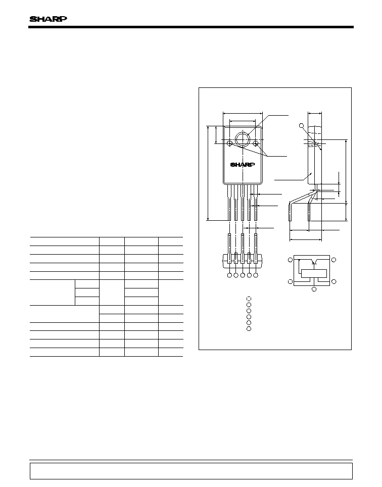
Outline Dimensions
(Unit : mm)
PQ5EV3
(25.2)
(4.5)
10.2
MAX.
3.5
±
0.2
5-0.7
±0.
1
3.2
±
0
.
5
(5.0)
8.2
±
0
.
7
4-(1.7)
2-(
1.4)
3.2
±
0.1
(6.6)
Epoxy resin
2-1.05
+
0.3
-
0
(2.0)
(1.0)
(0.6)
17.0
±0.
7
4.4
MIN.
5
4
3
2
1
5
4
3
2
1
6
DC input (V
IN
)
DC output (V
O
)
GND
Output voltage adjustment terminal (V
ADJ
)
ON/OFF control terminal (V
C
)
DC output(V
O
)
( ) : Typical dimensions
1
2
3
4
5
6
Specific IC
Parameter
Symbol
Rating
Unit
Input voltage
7
V
5.0
A
7.5
4
7
5
V
V
V
3.5
Output current
1.6
W
45
W
150
∞C
Power dissipation
Dropout voltage
Output control voltage
Output adjustment terminal voltage
V
IN
V
I-O
V
C
V
ADJ
I
O
P
D2
P
D1
(Ta
=
25
∞
C)
Junction temperature
Operating temperature
Storage temperature
Soldering temperature
T
j
-
20 to
+
80
∞C
T
opr
-
40 to
+
150
∞C
T
stg
260
∞C
T
sol
*1
*1
*1
*3
*4
*2
*1 All are open except GND and applicable terminals
*2 P
D1
:No heat sink, P
D2
:With infinite heat sink
*3 Overheat protection may operate at the condition T
j
:125∞C to 150∞C
*4 For 10s
PQ5EV3
PQ5EV5
PQ5EV7
1. Personal computers
2. Power supplies for various electronic equipment such as AV
or OA
s
Features
s
Applications
Large Output Current Type
Low Power-Loss Voltage Regulator
1. Low power-loss
(Dropout voltage: MAX.0.5V)
2. Package with exposed radiation fin
(Equivalent to TO-220)
3. Large output current
3.5A:
PQ5EV3
, 5A:
PQ5EV5
, 7.5A:
PQ5EV7
4. Variable output voltage (1.5V to 5V)
5. High-precision output type
(Reference voltage precision:
±
1.0%)
6. Overcurrent, overheat protection functions
Notice
In the absence of confirmation by device specification sheets, SHARP takes no responsibility for any defects that may occur in equipment using any SHARP
devices shown in catalogs, data books, etc. Contact SHARP in order to obtain the latest device specification sheets before using any SHARP device.
Internet
Internet address for Electronic Components Group http://www.sharp.co.jp/ecg/
PQ5EV3/PQ5EV5/PQ5EV7
2.35
-
7
1.5
1.2276
-
1.24
-
0.1
0.5
-
0.05
0.1
-
60
-
-
-
-
-
±
1
70
-
-
-
Parameter
MIN.
TYP.
MAX.
Conditions
(Unless otherwise specified, V
IN
=5V,
*5
,V
O
=3V (R
1
=2k
) , Ta=25∞C)
-
-
I
O
=5mA to rating
V
IN
=4 to 7V, I
O
=5mA
Refer to Fig.2
-
V
C
=2.7V
-
-
T
j
=0 to 125∞C
*6
*7
V
C
=0.4V
I
O
=0A
2
-
5
1.2524
-
-
0.5
-
20
0.8
-
0.4
Input voltage
Load line regulation
Input line regulation
Reference voltage temperature coefficient
Ripple Rejection
Dropout voltage
Output on control voltage
Output off control voltage
Output off control current
Non-operating dissipatiion current
Output on control current
Output voltage
Reference voltage
10
V
IN
V
O
V
ref
R
eg
L
R
eg
I
T
C
V
ref
RR
V
C (ON)
V
I-O
I
C (ON)
V
C (OFF)
I
C (OFF)
Symbol
I
q
V
V
V
%
%
dB
%
V
V
mA
V
µ
A
Unit
mA
-
15
*5
PQ5EV3
:I
O
=1.75A,
PQ5EV5
:I
O
=2.5A,
PQ5EV7
:I
O
=3.75A
*6
PQ5EV3
:I
O
=3.5A,
PQ5EV5
:I
O
=5A,
PQ5EV7
:I
O
=7.5A. Input voltage shall be the value when output voltage is 95% in comparison with the initial value
*7 In case of opening control terminal 5, output voltage turns on.
s
Electrical Characteristics
V
O
V
O
=
V
ref
◊
(1
+
R
2
/R
1
)
=
1.24
◊
(1
+
R
2
/R
1
)
[R
1
=
2k
,
V
ref
.=.
1.24V]
V
ref
I
O
I
q
R
L
R
2
V
C
V
IN
R
1
2k
100
µ
F
100
µ
F
+
+
V
A
V
A
A
2
1
5
4
3
I
O
eo
R
L
R
2
V
IN
ei
R
1
2k
100
µ
F
100
µ
F
2.7V
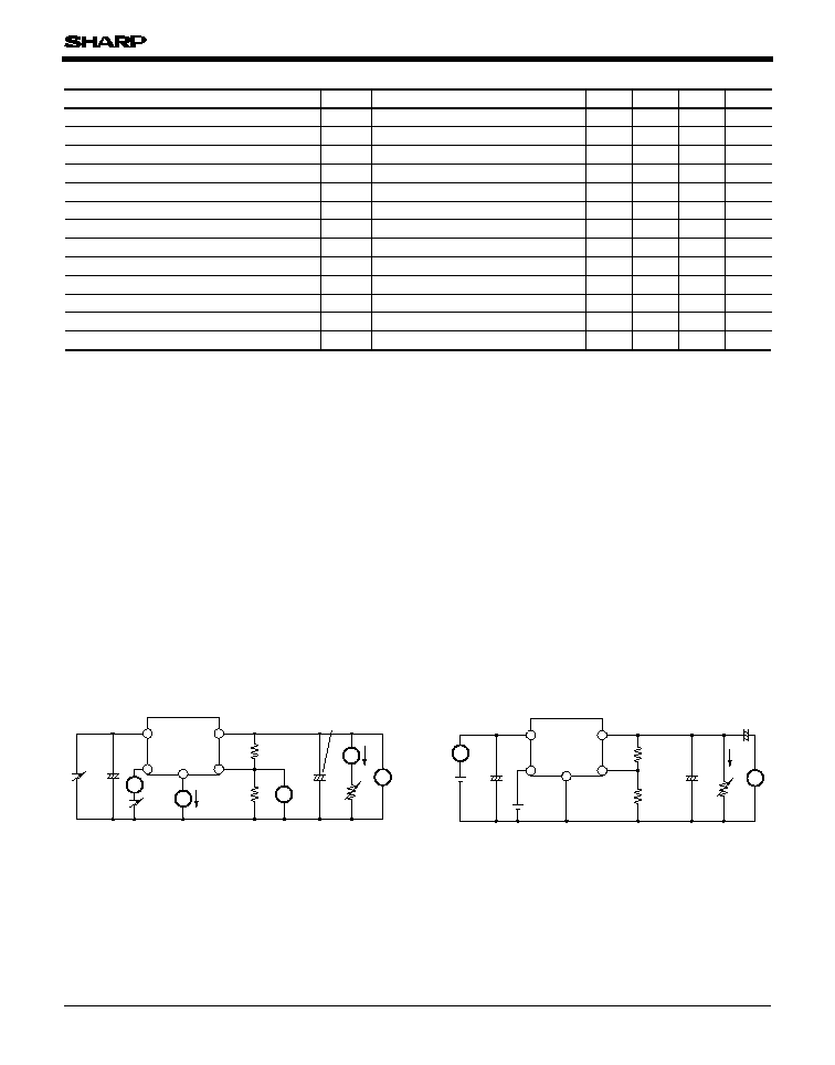
+
+
f
=
120Hz (sine wave)
ei(rms)
=
0.5V
V
O
=
3V (R
1
=
2k
)
V
IN
=
5V
I
O
=
0.5A
RR
=
20log (ei(rms)/eo(rms))
2
1
5
4
3
+
V
~
~
Fig.1
Standard Test Circuit
Fig.2
Test Circuit for Ripple Rejection
PQ5EV3/PQ5EV5/PQ5EV7
0
20
40
60
80
100
0
2
4
1
3
5
7
9
11
6
8
10
12
Output current I
O
(A)
V
I-O
=
3.7V
V
I-O
=
1.7V
V
I-O
=
1V
V
I-O
=
0.5V
Relative output voltage (%)
0
20
40
60
80
100
0
2
4
1
3
5
7
9
11
6
8
10
12
Output current I
O
(A)
V
I-O
=
3.7V
V
I-O
=
1.7V
V
I-O
=
1V
V
I-O
=
0.5V
Relative output voltage (%)
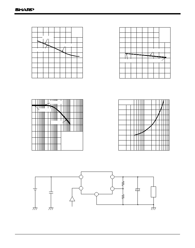
Fig.5 Overcurrent Protection Characteristics
(PQ5EV5)
Fig.6 Overcurrent Protection Characteristics
(PQ5EV7)
Relative output voltage (%)
0
20
40
60
80
100
0
2
4
1
3
5
7
9
11
6
8
10
12
Output current I
O
(A)
V
I-O
=
3.7V
V
I-O
=
1.7V
V
I-O
=
1V
V
I-O
=
0.5V
Power dissipation P
D
(W)
1.6
10
20
30
40
50
45
-
20
0
25
50
80
Ambient temperature T
a
(
∞
C)
P
D2
: With infinite heat sink
P
D1
: No heat sink
Note) Oblique line prtion:Overheat protection may operate in this area
Fig.4 Overcurrent Protection Characteristics
(PQ5EV3)
Fig.3 Power Dissipation vs. Ambient
Temperature
Output voltage V
O
(V)
Input voltage V
IN
(V)
0
1
2
3
4
0
3
6
1
4
7
2
5
R
L
=
1.7
R
L
=
R
1
=
2k
R
2
=
2.8k
R
L
=
0.8
V
IN
=
5V
I
O
=
0
V
O
=
3V
Reference voltage fluctuation
V
ref
(mV)
-
10
-
8
-
6
-
4
-
2
0
2
4
6
8
10
-
25
0
25
50
75
100
125
Junction temperature T
j
(
∞
C)
PQ5EV7
PQ5EV3
PQ5EV5
Fig.8 Output Voltage vs. Input Voltage
(PQ5EV3)
Fig.7 Reference Voltage Fluctuation vs.
Junction Temperature
PQ5EV3/PQ5EV5/PQ5EV7
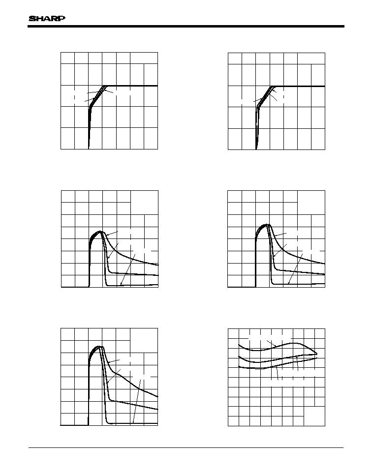
Circuit operating current I
BIAS
(mA)
Input voltage V
IN
(V)
0
20
40
60
80
100
120
140
160
0
1
2
3
4
5
6
7
R
1
=
2k
R
2
=
2.8k
(V
O
=
3V)
R
L
=
R
L
=
0.8
R
L
=
1.7
Circuit operating current I
BIAS
(mA)
Input voltage V
IN
(V)
0
20
40
60
80
100
120
140
160
0
1
2
3
4
5
6
7
R
L
=
R
1
=
2k
R
2
=
2.8k
(V
O
=
3V)
R
L
=
0.6
R
L
=
1.2
Fig.11 Circuit Operating Current vs.
Input Voltage (PQ5EV3)
Fig.12 Circuit Operating Current vs.
Input Voltage (PQ5EV5)
Output voltage V
O
(V)
Input voltage V
IN
(V)
0
1
2
3
4
0
3
6
1
4
7
2
5
R
L
=
R
1
=
2k
R
2
=
2.8k
R
L
=
0.8
R
L
=
0.4
Output voltage V
O
(V)
Input voltage V
IN
(V)
0
1
2
3
4
0
3
6
1
4
7
2
5
R
L
=
1.2
R
L
=
R
L
=
0.6
R
1
=
2k
R
2
=
2.8k
Fig.10 Output Voltage vs. Input Voltage
(PQ5EV7)
Fig.9 Output Voltage vs. Input Voltage
(PQ5EV5)
Dropout voltage V
I-O
(V)
0
0.05
0.1
0.15
0.2
0.25
0.3
0.35
0.4
0.45
0.5
-
40
0
100
140
40
80
120
60
20
-20
Junction temperature T
j
(
∞
C)
V
IN
=
5V
V
O
=
3V
PQ5EV7
: I
O
=7.5
A
PQ5EV5
: I
O
=5.0
A
PQ5EV3
: I
O
=3.5
A
Circuit operating current I
BIAS
(mA)
Input voltage V
IN
(V)
20
0
40
60
80
100
120
140
160
0
1
2
3
4
5
6
7
R
1
=
2k
R
2
=
2.8k
(V
O
=
3V)
R
L
=
R
L
=
0.8
R
L
=
0.4
Fig.14 Dropout Voltage vs. Junction
Temperature
Fig.13 Circuit Operating Current vs.
Input Voltage (PQ5EV7)
PQ5EV3/PQ5EV5/PQ5EV7
Ripple Rejection RR (dB)
0.1
1
10
100
1000
Input Ripple Frequency f (kHz)
0
10
20
30
40
50
60
70
80
ei(rms)
=0.
5V
V
OUT
=
3V
I
O
=
0.5V
C
OUT
=
100
µ
F
C
IN
=
0
V
IN
=
5V
PQ5EV3
PQ5EV5
PQ5EV7
Fig.17 Ripple Rejection vs. Input Ripple
Frequency
Output voltage V
O
(V)
R
2
(
)
0
0.5
1
1.5
2
2.5
3
3.5
4
4.5
5
100
1 000
10 000
R
1
=
2k
Fig.18 Output Voltage Adjustment
Characteristics
Non-operating dissipatiion current (mA)
0.5
1
1.5
2
2.5
3
3.5
4
4.5
5
-
40
0
100
140
40
80
120
60
20
-
20
Junction temperature T
j
(
∞
C)
0
V
IN
=
5V
I
O
=
0V
V
O
=
3V
V
C
=
2V
PQ5EV3
PQ5EV7
PQ5EV5
ON/OFF threshold voltage (V)
0
0.2
0.4
0.6
0.8
1
1.2
1.4
1.6
1.8
2
-
40
0
100
140
40
80
120
60
20
-
20
Junction temperature T
j
(
∞
C)
PQ5EV7
V
IN
=
5V
I
O
=
0V
V
O
=
3V
PQ5EV3
PQ5EV5
Fig.16 Non-operating Dissipatiion Current
vs. Junctiion Temperature
Fig.15 ON-OFF Threshold Voltage vs.
Junction Temperature
1
2
5
3
4
V
O
V
IN
R
2
C
IN
R
1
C
O
+
C-MOS or TTL
Load
Fig.19 External Connection
PQ5EV3/PQ5EV5/PQ5EV7
s
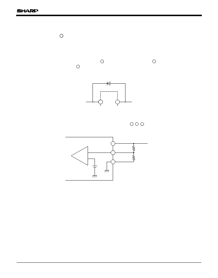
Precautions for Use
1. The connecting wiring of C
O
and each terminal must be as short as possible. Owing to type, value and wiring condition of
capacitor, it may oscillate. Confirm the output waveform under the actual condition before using.
2. ON/OFF control terminal is compatible with LS-TTL. It enables to be directly drive by TTL or C-MOS standard logic
(RCA4000 series) . If ON/OFF control terminal is not used, it is recommended to directly connect applicable terminals with input
terminal.
3. If voltage is applied under the conditions that the device pin is connected divergently or reversely, the deterioration of
characteristics or damage may occur. Never allow improper mounting.
4. If voltage exceeding the voltage of DC input terminal is applied to the output terminal , the element may be damaged.
Especially when the DC input terminal is short-circuited to the GND in ordinary operating state, charges accumulated in the
output capacitor C
O
flow to the input side, causing damage to the element. In this case, connect the ordinary silicon diode as shown
in the figure.
1
2
5
1. Output voltage is able to set (1.5V to 5V) when resistors R
1
, R
2
are attached to , , terminals. As for the external resistors to
set output voltage, refer to the following figure and Fig.18.
2
3
4
1
2
1
2
4
3
R
2
V
O
R
1
V
ref
-
+
V
O
=
V
ref
◊
(1
+
R
2
/R
1
)
=
1.24
◊
(1
+
R
2
/2000)
[R
1
=
2k
,
V
ref
.=.
1.24V]
s
Adjustment of Output Voltage

115
Application Circuits
NOTICE
qThe circuit application examples in this publication are provided to explain representative applications of
SHARP devices and are not intended to guarantee any circuit design or license any intellectual property
rights. SHARP takes no responsibility for any problems related to any intellectual property right of a
third party resulting from the use of SHARP's devices.
qContact SHARP in order to obtain the latest device specification sheets before using any SHARP device.
SHARP reserves the right to make changes in the specifications, characteristics, data, materials,
structure, and other contents described herein at any time without notice in order to improve design or
reliability. Manufacturing locations are also subject to change without notice.
qObserve the following points when using any devices in this publication. SHARP takes no responsibility
for damage caused by improper use of the devices which does not meet the conditions and absolute
maximum ratings to be used specified in the relevant specification sheet nor meet the following
conditions:
(i) The devices in this publication are designed for use in general electronic equipment designs such as:
--- Personal computers
--- Office automation equipment
--- Telecommunication equipment [terminal]
--- Test and measurement equipment
--- Industrial control
--- Audio visual equipment
--- Consumer electronics
(ii)Measures such as fail-safe function and redundant design should be taken to ensure reliability and
safety when SHARP devices are used for or in connection with equipment that requires higher
reliability such as:
--- Transportation control and safety equipment (i.e., aircraft, trains, automobiles, etc.)
--- Traffic signals
--- Gas leakage sensor breakers
--- Alarm equipment
--- Various safety devices, etc.
(iii)SHARP devices shall not be used for or in connection with equipment that requires an extremely
high level of reliability and safety such as:
--- Space applications
--- Telecommunication equipment [trunk lines]
--- Nuclear power control equipment
--- Medical and other life support equipment (e.g., scuba).
qContact a SHARP representative in advance when intending to use SHARP devices for any "specific"
applications other than those recommended by SHARP or when it is unclear which category mentioned
above controls the intended use.
qIf the SHARP devices listed in this publication fall within the scope of strategic products described in the
Foreign Exchange and Foreign Trade Control Law of Japan, it is necessary to obtain approval to export
such SHARP devices.
qThis publication is the proprietary product of SHARP and is copyrighted, with all rights reserved. Under
the copyright laws, no part of this publication may be reproduced or transmitted in any form or by any
means, electronic or mechanical, for any purpose, in whole or in part, without the express written
permission of SHARP. Express written permission is also required before any use of this publication
may be made by a third party.
qContact and consult with a SHARP representative if there are any questions about the contents of this
publication.