ChipFind - документация

Электронный компонент: S1ZAS4

Скачать:  PDF   ZIP
S1ZAS4
40V 1.2A
Copyright & Copy;2000 Shindengen Electric Mfg.Co.Ltd
OUTLINE DIMENSIONS
RATINGS
SHINDENGEN
i
Unit : mm
Switching power supply
DC/DC converter
Home Appliances, Office Equipment
Telecommunication
APPLICATION
SMT
Tj150
P
RRSM
avalanche guaranteed
Array
FEATURES
Case : 1Z
Dual
Schottky Rectifiers (SBD)
Absolute Maximum Ratings (If not specified Tl=25)
Item
Symbol
Conditions
Ratings
Unit
Storage Temperature
Tstg
-40150
Operating Junction Temperature
Tj
150
Maximum Reverse Voltage
V
RM
40
V
Repetitive Peak Surge Reverse Voltage
V
RRSM
Pulse width 0.5ms, duty 1/40
45
V
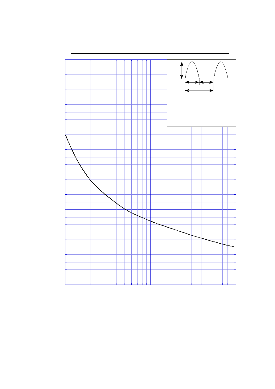
50Hz sine wave, R-load, On alumina substrate, 1 element operation, Ta=49
1.2
Average Rectified Forward Current
I
O
50Hz sine wave, R-load, On alumina substrate, 2 element operation, Ta=45
0.9*
A
50Hz sine wave, R-load, On glass-epoxy substrate, 1 element operation, Ta=47
1.0
50Hz sine wave, R-load, On glass-epoxy substrate, 2 element operation, Ta=43
0.72*
Peak Surge Forward Current
I
FSM
50Hz sine wave, Non-repetitive 1 cycle peak value, Tj=125
40
A
Repetitive Peak Surge Reverse Power
P
RRSM
Pulse width 10s, Rating of per diode, Tj=25
160
W
Electrical Characteristics (If not specified Tl=25)
Item
Symbol
Conditions
Ratings
Unit
Forward Voltage
V
F
I
F
=1A, Pulse measurement, Rating of per diode
Max.0.55
V
Reverse Current
I
R
V
R
=V
RM
, Pulse measurement, Rating of per diode
Max.1
mA
Junction Capacitance
Cj
f=1MHz, V
R
=10V, Rating of per diode
Typ.65
pF
jl
junction to lead
Max.25
junction to ambient, On alumina substrate, 1 element operation
Max.93
Thermal Resistance
ja
junction to ambient, On alumina substrate, 2 element operation
Max.140* /W
junction to ambient, On glass-epoxy substrate, 1 element operation
Max.120
junction to ambient, On glass-epoxy substrate, 2 element operation
Max.186*
Raitng of per diode
Forward Voltage
0.01
0.1
1
10
0
0.2
0.4
0.6
0.8
1
1.2
1.4
1.6
S1ZAS4
Tl=150
C [MAX]
Tl=25
C [MAX]
Pulse measurement per diode
Tl=150
C [TYP]
Tl=25
C [TYP]
Forward Voltage V
F
[V]
Forward Current I
F
[A]
10
100
S1ZAS4
0.1
1
10
0.05
0.5
0.2
20
50
5
2
200
500
2000
5000
0.02
0.05
0.5
0.2
20
5
2
0.005
0.002
Reverse Voltage V
R
[V]
Junction Capacitance Cj [pF]
f=1MHz
Tl=25
C
TYP
per diode
Junction Capacitance
Reverse Current
0.01
0.1
1
10
100
1000
0
5
10
15
20
25
30
35
40
S1ZAS4
Tl=150
C [MAX]
Tl=150
C [TYP]
Pulse measurement per diode
Tl=125
C [TYP]
Tl=100
C [TYP]
Tl=75
C [TYP]
Reverse Voltage V
R
[V]
Reverse Current I
R
[mA]
0
0.5
1
1.5
2
2.5
0
10
20
30
40
50
S1ZAS4
0.3
Reverse Power Dissipation
Tj = 150
C
SIN
0.2
0.5
D=0.05
DC
0.1
0.8
Reverse Voltage V
R
[V]
Reverse Power Dissipation P
R
[W]
per diode
0
t
p
V
R
T
D=t
p
/T
0
t
p
I
O
T
D=t
p
/T
0
0.5
1
1.5
2
0
0.5
1
1.5
2
S1ZAS4
0.3
Forward Power Dissipation
Tj = 150
C
SIN
0.2
0.1
D=0.8
DC
0.5
0.05
per diode
Average Rectified Forward Current I
O
[A]
Forward Power Dissipation P
F
[W]
0
t
p
I
O
T
D=t
p
/T
0
0.5
1
1.5
2
2.5
0
20
40
60
80
100
120
140
160
S1ZAS4
0.3
Derating Curve
V
R
= 20V
SIN
0.2
0.1
D=0.8
DC
0.5
0.05
0
V
R
Alumina substrate
Soldering land 1mm
Conductor layer 20
m
Substrate thickness 0.64mm
1-element conduction
Ambient Temperature Ta [
C]
Average Rectified Forward Current I
O
[A]
0
t
p
I
O
T
D=t
p
/T
0
0.5
1
1.5
2
0
20
40
60
80
100
120
140
160
S1ZAS4
0.3
Derating Curve
V
R
= 20V
SIN
0.2
0.1
D=0.8
DC
0.5
0.05
0
V
R
2-element conduction,
per diode
Ambient Temperature Ta [
C]
Average Rectified Forward Current I
O
[A]
Alumina substrate
Soldering land 1mm
Conductor layer 20
m
Substrate thickness 0.64mm
0
t
p
I
O
T
D=t
p
/T
0
0.5
1
1.5
2
0
20
40
60
80
100
120
140
160
S1ZAS4
0.3
Derating Curve
V
R
= 20V
SIN
0.2
0.1
D=0.8
DC
0.5
0.05
0
V
R
1-element conduction
Glass-epoxy substrate
Soldering land 1mm
Conductor layer 35
m
Ambient Temperature Ta [
C]
Average Rectified Forward Current I
O
[A]
0
t
p
I
O
T
D=t
p
/T
0
0.2
0.4
0.6
0.8
1
1.2
1.4
1.6
0
20
40
60
80
100
120
140
160
S1ZAS4
0.3
Derating Curve
V
R
= 20V
SIN
0.2
0.1
D=0.8
DC
0.5
0.05
0
V
R
2-element conduction,
per diode
Ambient Temperature Ta [
C]
Average Rectified Forward Current I
O
[A]
Glass-epoxy substrate
Soldering land 1mm
Conductor layer 35
m
Peak Surge Forward Capability
0
10
20
30
40
50
60
1
10
100
S1ZAS4
2
5
20
50
I
FSM
10ms 10ms
1 cycle
Number of Cycles [cycles]
Peak Surge Forward Current I
FSM
[A]
non-repetitive,
sine wave,
Tj=125
C before
surge current is applied
t
p
I
RP
0
V
R
0.5I
RP
V
RP
I
R
P
RRSM
= I
RP
V
RP
0
20
40
60
80
100
120
0
50
100
150
SBD
Repetitive Surge Reverse Power Derating Curve
Junction Temperature Tj [
C]
P
RRSM
Derating [%]
0.1
1
10
1
10
100
SBD
Repetitive Surge Reverse Power Capability
Pulse Width t
p
[
s]
P
RRSM
(t
p
) / P
RRSM
(t
p
=10
s) Ratio
t
p
I
RP
0
V
R
0.5I
RP
V
RP
I
R
P
RRSM
= I
RP
V
RP