Semiconductor Group
1
Mar-29-1996
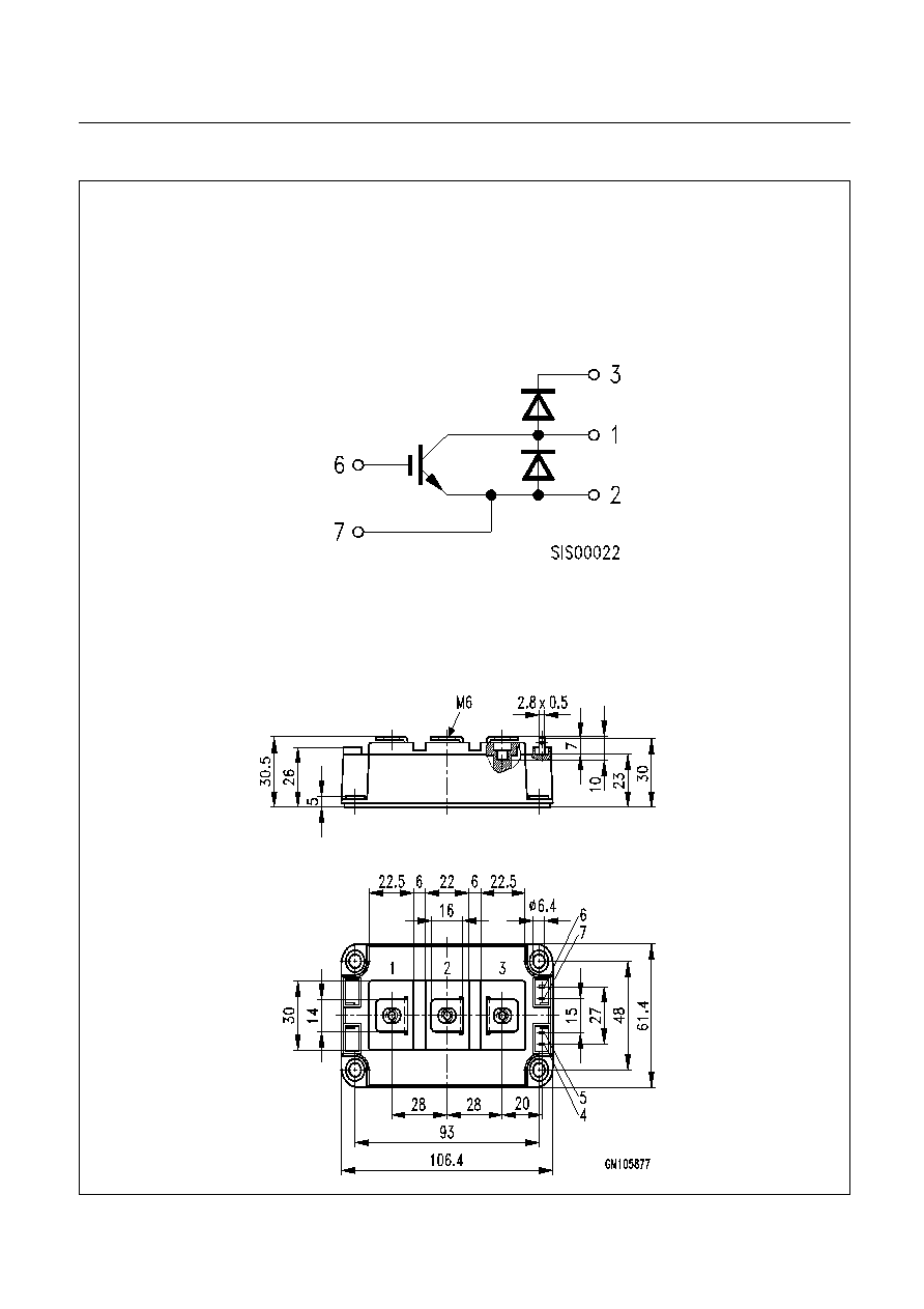
BSM 100 GAL 120 DN2
IGBT Power Module
∑ Single switch with chopper diode
∑ Including fast free-wheeling diodes
∑ Package with insulated metal base plate
Type
V
CE
I
C
Package
Ordering Code
BSM 100 GAL 120 DN2
1200V 150A
HALF BRIDGE GAL 2
C67076-A2012-A70
Maximum Ratings
Parameter
Symbol
Values
Unit
Collector-emitter voltage
V
CE
1200
V
Collector-gate voltage
R
GE
= 20 k
V
CGR
1200
Gate-emitter voltage
V
GE
± 20
DC collector current
T
C
= 25 ∞C
T
C
= 80 ∞C
I
C
100
150
A
Pulsed collector current,
t
p
= 1 ms
T
C
= 25 ∞C
T
C
= 80 ∞C
I
Cpuls
200
300
Power dissipation per IGBT
T
C
= 25 ∞C
P
tot
800
W
Chip temperature
T
j
+ 150
∞C
Storage temperature
T
stg
-55 ... + 150
Thermal resistance, chip case
R
thJC
0.16
K/W
Diode thermal resistance, chip case
R
thJCD
0.3
Diode thermal resistance, chip-case,chopper
R
THJCDC
0.25
Insulation test voltage,
t
= 1min.
V
is
2500
Vac
Creepage distance
-
20
mm
Clearance
-
11
DIN humidity category, DIN 40 040
-
F
-
IEC climatic category, DIN IEC 68-1
-
55 / 150 / 56

Semiconductor Group
2
Mar-29-1996
BSM 100 GAL 120 DN2
Electrical Characteristics, at T
j
= 25 ∞C, unless otherwise specified
Parameter
Symbol
Values
Unit
min.
typ.
max.
Static Characteristics
Gate threshold voltage
V
GE
=
V
CE,
I
C
= 4 mA
V
GE(th)
4.5
5.5
6.5
V
Collector-emitter saturation voltage
V
GE
= 15 V,
I
C
= 100 A,
T
j
= 25 ∞C
V
GE
= 15 V,
I
C
= 100 A,
T
j
= 125 ∞C
V
CE(sat)
-
-
2.5
3.1
3
3.7
Zero gate voltage collector current
V
CE
= 1200 V,
V
GE
= 0 V,
T
j
= 25 ∞C
V
CE
= 1200 V,
V
GE
= 0 V,
T
j
= 125 ∞C
I
CES
-
-
6
1.5
-
2
mA
Gate-emitter leakage current
V
GE
= 20 V,
V
CE
= 0 V
I
GES
-
-
200
nA
AC Characteristics
Transconductance
V
CE
= 20 V,
I
C
= 100 A
g
fs
54
-
-
S
Input capacitance
V
CE
= 25 V,
V
GE
= 0 V,
f
= 1 MHz
C
iss
-
6.5
-
nF
Output capacitance
V
CE
= 25 V,
V
GE
= 0 V,
f
= 1 MHz
C
oss
-
1
-
Reverse transfer capacitance
V
CE
= 25 V,
V
GE
= 0 V,
f
= 1 MHz
C
rss
-
0.5
-

Semiconductor Group
3
Mar-29-1996
BSM 100 GAL 120 DN2
Electrical Characteristics, at T
j
= 25 ∞C, unless otherwise specified
Parameter
Symbol
Values
Unit
min.
typ.
max.
Switching Characteristics, Inductive Load at
T
j
= 125 ∞C
Turn-on delay time
V
CC
= 600 V,
V
GE
= 15 V,
I
C
= 100 A
R
Gon
= 6.8
t
d(on)
-
130
260
ns
Rise time
V
CC
= 600 V,
V
GE
= 15 V,
I
C
= 100 A
R
Gon
= 6.8
t
r
-
80
160
Turn-off delay time
V
CC
= 600 V,
V
GE
= -15 V,
I
C
= 100 A
R
Goff
= 6.8
t
d(off)
-
400
600
Fall time
V
CC
= 600 V,
V
GE
= -15 V,
I
C
= 100 A
R
Goff
= 6.8
t
f
-
70
100
Free-Wheel Diode
Diode forward voltage
I
F
= 100 A,
V
GE
= 0 V,
T
j
= 25 ∞C
I
F
= 100 A,
V
GE
= 0 V,
T
j
= 125 ∞C
V
F
-
-
1.8
2.3
-
2.8
V
Reverse recovery time
I
F
= 100 A,
V
R
= -600 V,
V
GE
= 0 V
d
i
F
/
dt
= -1000 A/µs,
T
j
= 125 ∞C
t
rr
-
0.3
-
µs
Reverse recovery charge
I
F
= 100 A,
V
R
= -600 V,
V
GE
= 0 V
d
i
F
/
dt
= -1000 A/µs
T
j
= 25 ∞C
T
j
= 125 ∞C
Q
rr
-
-
14
4
-
-
µC

Semiconductor Group
4
Mar-29-1996
BSM 100 GAL 120 DN2
Electrical Characteristics, at T
j
= 25 ∞C, unless otherwise specified
Parameter
Symbol
Values
Unit
min.
typ.
max.
Chopper Diode
Chopper diode forward voltage
I
FC
= 150 A,
V
GE
= 0 V,
T
j
= 25 ∞C
I
FC
= 150 A,
V
GE
= 0 V,
T
j
= 125 ∞C
V
FC
-
-
1.8
2.3
-
2.8
V
Reverse recovery time, chopper
I
FC
= 150 A,
V
R
= -600 V,
V
GE
= 0 V
d
i
F
/
dt
= -1500 A/µs,
T
j
= 125 ∞C
t
rrC
-
0.4
-
µs
Reverse recovery charge, chopper
I
FC
= 150 A,
V
R
= -600 V,
V
GE
= 0 V
d
i
F
/
dt
= -1500 A/µs
T
j
= 25 ∞C
T
j
= 125 ∞C
Q
rrC
-
-
18
5
-
-
µC