 | –≠–ª–µ–∫—Ç—Ä–æ–Ω–Ω—ã–π –∫–æ–º–ø–æ–Ω–µ–Ω—Ç: CGY196 | –°–∫–∞—á–∞—Ç—å:  PDF PDF  ZIP ZIP |
CGY 196
Siemens Aktiengesellschaft
1
16.6.1998
HL HF PE GaAs
GaAs MMIC
Preliminary Data
l
Broadband Power Amplifier [ 800..3500 Mhz ]
l
DECT,PHS,PCS,GSM,AMPS,WLAN,WLL
l
Single Voltage Supply
l
Operating voltage range: 2.0to 6 V
l
Pout = 25.5dBm at Vd=2.4V
l
Pout = 27.0dBm at Vd=3.0V
l
Pout = 30.0dBm at Vd=5.0V
l
Overall power added efficiency up to 50 %
l
Easy external matching
ESD: Electrostatic discharge sensitive device,
observe handling precautions!
Type
Marking
Ordering code
(taped)
Package
CGY 196
t.b.d.
t.b.d.
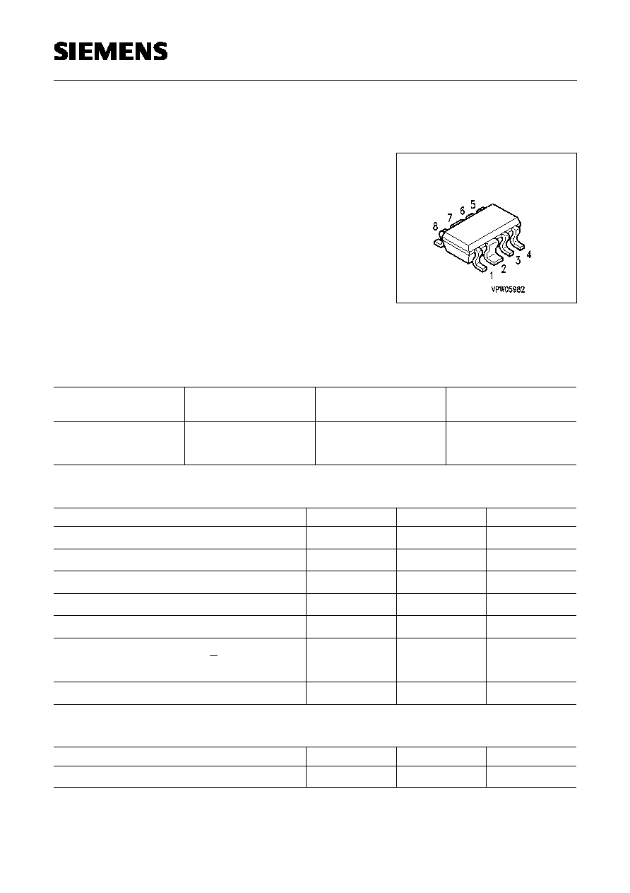
SCT598
Maximum ratings
Characteristics
Symbol
max. Value
Unit
Positive supply voltage
VD
6
V
Supply current
ID
1.0
A
Maximum input power
Pinmax
20
dBm
Channel temperature
TCh
150
∞C
Storage temperature
Tstg
-55...+150
∞C
Total power dissipation
(Ts < 81 ∞C)
Ts: Temperature at soldering point
Ptot
1.0
W
Pulse peak power
PPulse
2.0
W
Thermal Resistance
Characteristics
Symbol
max. Value
Unit
Channel-soldering point
RthChS
70
K/W
Semiconductor Group
1
1998-11-01
CGY 196
Siemens Aktiengesellschaft
2
16.6.1998
HL HF PE GaAs
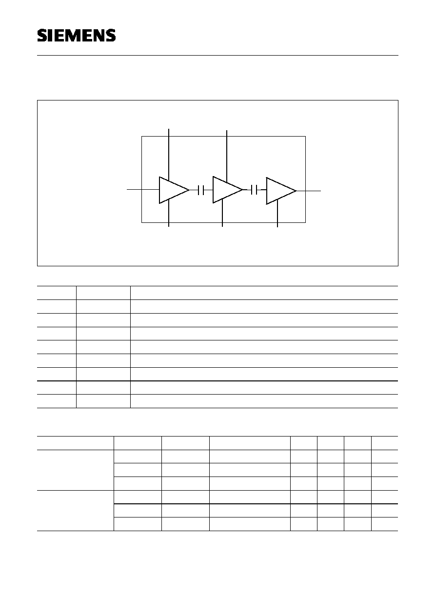
Functional Block Diagram
Pin #
Name
Configuration
1
RFin/Vg
RF input power + Gate voltage [0V internal]
2
GND
RF and DC ground
3
VD2
Pos. drain voltage of the 2nd stage
4
n.c.
not connected
5
n.c.
not connected
6
RFout/VD3 RF output power / Pos. drain voltage of the 3rd stage
7
GND
RF and DC ground
8
VD1
Pos. drain voltage of the 1st stage
DC characteristics
Characteristics
Symbol
Conditions
min
typ
max
Unit
stage 1
IDSS1
VD1=3V
45
mA
stage 2
IDSS2
VD2=3V
65
mA
Drain current
stage 3
IDSS2
VD2=3V
340
mA
stage 1
gfs1
VD=3V, ID=50mA
110
mS
stage 2
gfs2
VD=3V, ID=300mA
650
mS
Transconductance
stage 3
gfs3
VD=3V, ID=300mA
650
mS
RFout/Vd3
RFin/Vg
VD2
VD1
G ND
G ND
G ND
Semiconductor Group
2
1998-11-01
CGY 196
Siemens Aktiengesellschaft
3
16.6.1998
HL HF PE GaAs
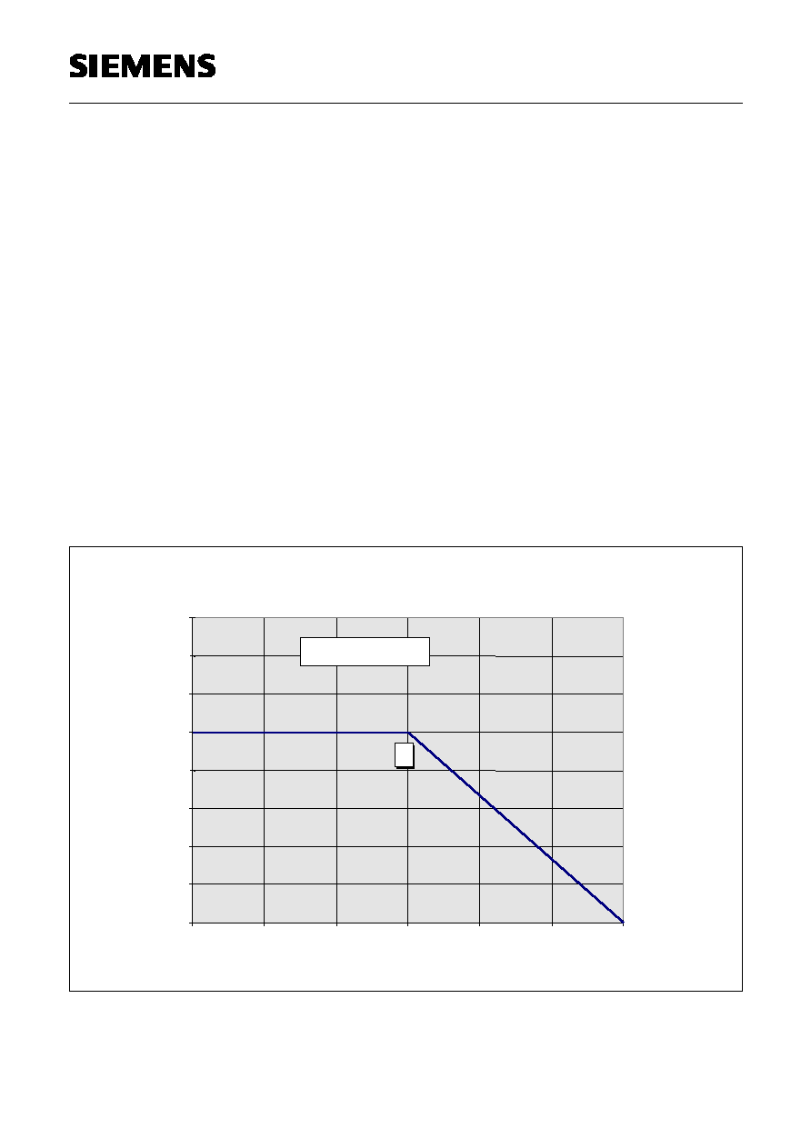
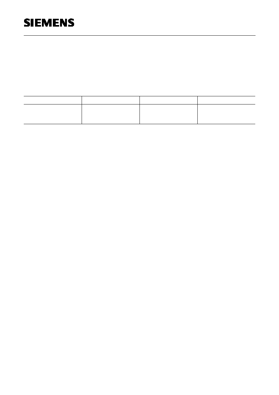
Permissible Total Power Dissipation in DC Operation
75
0
200
400
600
800
1000
1200
1400
1600
0
25
50
75
100
125
150
Temperature of soldering point, Ts ∞C
P
tot DC
= f (T
s
)
mW
Determination of Permissible Total Power Dissipation for Continuous and Pulse
Operation
The dissipated power is the power which remains in the chip and heats the device. It does
not contain RF signals which are coupled out consistently.
a) Continuous Wave / DC Operation
For the determination of the permissible total power dissipation P
tot-DC
from the diagram
below it is necessary to obtain the temperature of the soldering point T
S
first. There are two
cases:
∑
When
R
thSA
(soldering point to ambient) is not known: Measure T
S
with a temperature
sensor at the leads were the heat is transferred from the device to the board ( normally at
the widest source or ground lead for GaAs ). Use a small sensor of low heat transport,
for example a thermoelement ( < 1mm ) with thin wires or a temperature indicating paper
while the device is operating.
∑
When
R
thSA
is already known:
T
S
= P
diss
x R
thSA
+ T
A
Semiconductor Group
3
1998-11-01
CGY 196
Siemens Aktiengesellschaft
4
16.6.1998
HL HF PE GaAs
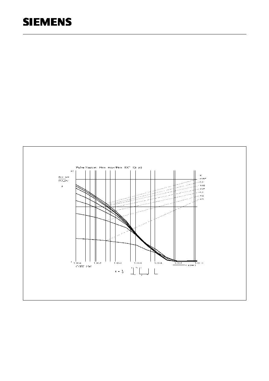
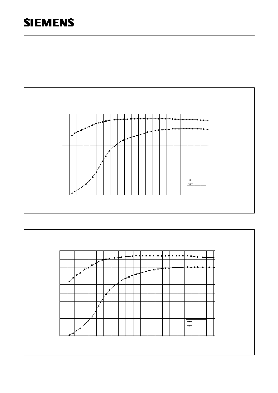
b) Pulsed Operation
For the calculation of the permissible pulse load P
tot-max
the following formula is applicable:
P
tot-max
= P
tot-DC
x Pulse factor
= P
tot-DC
x ( P
tot-max
/ P
tot-DC
)
Use the values for P
tot-DC
as derived from the above diagram and for the
pulse factor = P
tot-max
/ P
tot-DC
from the following diagram to get a specific value.
Pulse factor:
P
tot-max
should not exceed the absolute maximum rating for the dissipated power
P
Pulse
= " Pulse peak power " = 2 W
Semiconductor Group
4
1998-11-01
CGY 196
Siemens Aktiengesellschaft
5
16.6.1998
HL HF PE GaAs
c) Reliability Considerations
This procedure yields the upper limit for the power dissipation for continuous wave (cw) and
pulse applications which corresponds to the maximum allowed channel temperature. For
best reliability keep the channel temperature low. The following formula allows to track the
individual contributions which determine the channel temperature.
T
ch
=
( P
diss
x
R
thChS
) +
T
S
Channel temperature (=
junction temperature)
Power dissipated in the chip. It
does not contain decoupled RF-
power
Rth of device from channel to
soldering point
Temperature of soldering point,
measured or calculated
Semiconductor Group
5
1998-11-01

CGY 196
Siemens Aktiengesellschaft
6
16.6.1998
HL HF PE GaAs
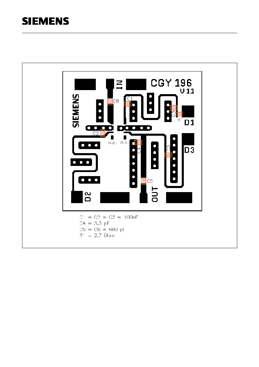
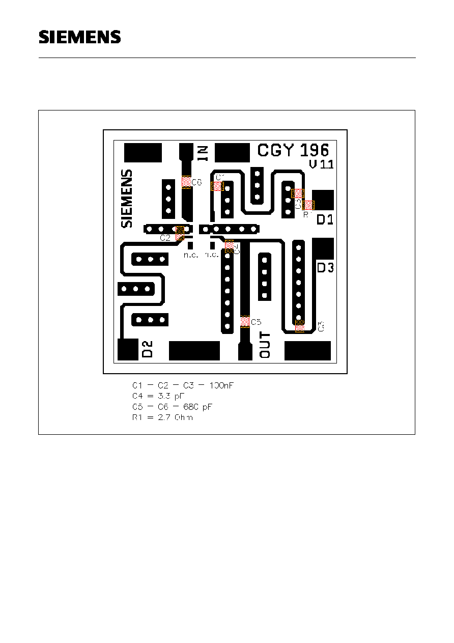
Electrical characteristics [ 3.0V DECT-Application: PCB-Layout see page 9]
(TA = 25∞C , f=1.89 GHz, ZS=ZL=50 Ohm, unless otherwise specified)
Characteristics
Symbol
min
typ
max
Unit
Supply current
VD=3.0V; Pin = +0 dBm
IDD
-
300
-
mA
Supply current
VD=3.0V; Pin = -10 dBm
IDD
-
450
-
mA
Gain
VD=3.0V; Pin = -10 dBm
G
32
dB
Output Power
VD=3.0V; Pin = 0 dBm
Po
26.0
dBm
Overall Power added Efficiency
VD=3.0V; Pin = +0 dBm
PAE
45
-
%
Overall Power added Efficiency
VD=3.0V; Pin = 3 dBm
PAE
50
-
%
Supply current
VD=4.8V; Pin = -10 dBm
IDD
-
450
-
mA
Supply current
VD=4.8V; Pin = 0 dBm
IDD
-
370
-
mA
Gain
VD=4.8V; Pin = -10 dBm
G
-
32
-
dB
Output Power
VD=4.8V; Pin = 0 dBm
Po
29
dBm
Overall Power added Efficiency
VD=4.8V; Pin = 0 dBm
PAE
45
-
%
Overall Power added Efficiency
VD=4.8V; Pin = 5 dBm
PAE
50
-
%
Off Isolation
VD=0V; Pin = 0 dBm
-S21
40
dB
Load mismatch
Pin=0dBm , VD
3.6
V , Z
S
=50 Ohm,
Load VSWR = 20:1 for all phase,
-
No module damage
for 10 sec.
-
Load mismatch
Pin=3dBm , VD
5.0V , Z
S
=50 Ohm,
Load VSWR = 20:1 for all phase,
-
No module damage
for 10 sec.
-
Stability
Pin=0dBm, VD=3.6V, Z
S
=50 Ohm,
Load VSWR = 3:1 for all phase
-
All spurious output
more than 70 dB below
desired signal level
-
Stability
Pin=3dBm , VD=5.0V , Z
S
=50 Ohm,
Load VSWR = 3:1 for all phase,
-
All spurious output
more than 70 dB below
desired signal level
-
Semiconductor Group
6
1998-11-01
CGY 196
Siemens Aktiengesellschaft
7
16.6.1998
HL HF PE GaAs
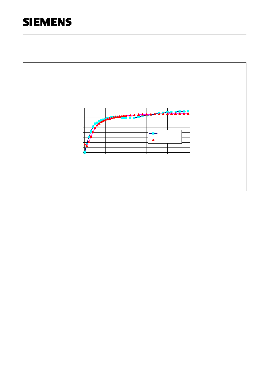
Output power and power added efficiency
pulsed mode: T=417
µ
s, duty cycle 12.5%
Electrical characteristics [3.0V DECT-Application: PCB-Layout see page 9]
CGY196
Vd=3.3V, duty cycle 10%
17,0
18,0
19,0
20,0
21,0
22,0
23,0
24,0
25,0
26,0
27,0
-11
-10
-9
-8
-7
-6
-5
-4
-3
-2
-1
0
1
2
3
4
5
6
7
8
9
10
Pin/dBm
10,0
15,0
20,0
25,0
30,0
35,0
40,0
45,0
50,0
55,0
60,0
Pout [dBm]
PAE [%]
CGY196
VD=5.0V, duty cycle 10%
20,0
21,0
22,0
23,0
24,0
25,0
26,0
27,0
28,0
29,0
30,0
-11
-10
-9
-8
-7
-6
-5
-4
-3
-2
-1
0
1
2
3
4
5
6
7
8
9
10
Pin/dBm
10,0
15,0
20,0
25,0
30,0
35,0
40,0
45,0
50,0
55,0
60,0
Pout [dBm]
PAE [%]
Semiconductor Group
7
1998-11-01
CGY 196
Siemens Aktiengesellschaft
8
16.6.1998
HL HF PE GaAs
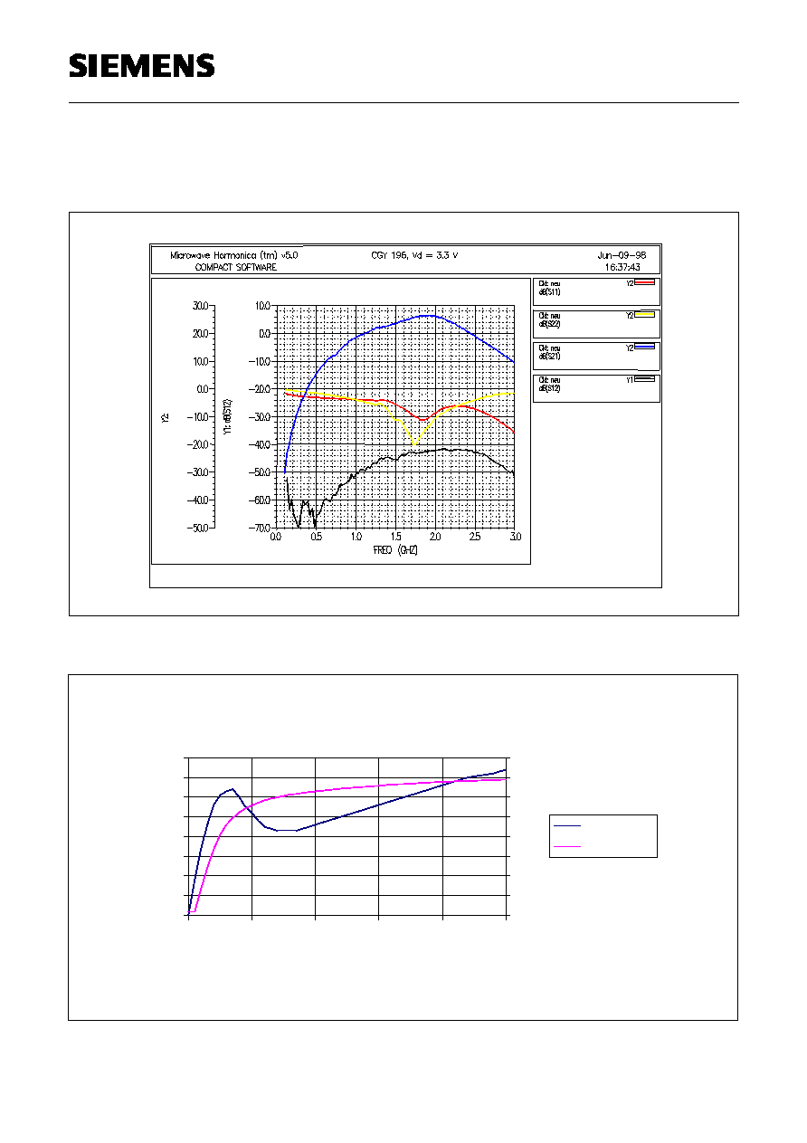
Electrical characteristics [3.0V DECT-Application: PCB-Layout see page 9]
S-Parameter [pulsed mode: T=417
µ
s, duty cycle 12.5%, Pin=0dBm,Vd=3.3V]
Pout,Id = f (Vd) | Pin=0dBm [pulsed mode: T=417
µ
s, duty cycle 12.5%]
CGY196
0
50
100
150
200
250
300
350
400
0,0
1,0
2,0
3,0
4,0
5,0
Vd / V
-40
-30
-20
-10
0
10
20
30
40
I(mA)
Pout(dBm)
+ + + + + + + +
+
+
+
+
+ + +
+
+
+
*
*
*
*
*
*
*
*
*
*
*
*
*
*
*
*
*
*
o
o
o
o
o
o
o
o o
o o o o
o
o
o
o
o
x
x
x
x
x
x
x
x x
x x x x x x
x
x
x
Semiconductor Group
8
1998-11-01
CGY 196
Siemens Aktiengesellschaft
9
16.6.1998
HL HF PE GaAs
Electrical characteristics [3.0V DECT-Application: PCB-Layout see page 9]
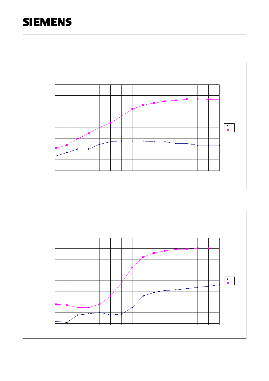
Harmonic Distortion
CGY196 Vd=3.3V
-70,0
-65,0
-60,0
-55,0
-50,0
-45,0
-40,0
-35,0
-30,0
-10
-9
-8
-7
-6
-5
-4
-3
-2
-1
0
1
2
3
4
5
Pin / dBm
D
i
stor
tion / dB
c
2f
3f
Harmonic Distortion
CGY196 Vd=4.8V
-70,0
-65,0
-60,0
-55,0
-50,0
-45,0
-40,0
-35,0
-30,0
-10
-9
-8
-7
-6
-5
-4
-3
-2
-1
0
1
2
3
4
5
Pin / dBm
D
i
stor
tion / dB
c
2f
3f
Semiconductor Group
9
1998-11-01
CGY 196
Siemens Aktiengesellschaft
10
16.6.1998
HL HF PE GaAs
Test Board Layout [3.0V DECT-Application f=1.89GHz ]
Semiconductor Group
10
1998-11-01
CGY 196
Siemens Aktiengesellschaft
11
16.6.1998
HL HF PE GaAs
Electrical characteristics [2.4V DECT-Application: PCB-Layout see page 12]
(TA = 25∞C , f=1.89 GHz, ZS=ZL=50 Ohm, unless otherwise specified)
Characteristics
Symbol
min
typ
max
Unit
Supply current
VD=2.4V; Pin = +0 dBm
IDD
-
360
-
mA
Supply current
VD=2.4V; Pin = -10 dBm
IDD
-
450
-
mA
Output Power
VD=2.4V; Pin = 0 dBm
Po
25.7
dBm
Overall Power added Efficiency
VD=2.4V; Pin = +0 dBm
PAE
44
-
%
Supply current
VD=2.2V; Pin = +0 dBm
IDD
-
350
-
mA
Supply current
VD=2.2V; Pin = -10 dBm
IDD
-
450
-
mA
Output Power
VD=2.2V; Pin = 0 dBm
Po
25.1
dBm
Overall Power added Efficiency
VD=2.2V; Pin = +0 dBm
PAE
42
-
%
Supply current
VD=3.0V; Pin = +0 dBm
IDD
-
370
-
mA
Supply current
VD=3.0V; Pin = -10 dBm
IDD
-
450
-
mA
Output Power
VD=3.0V; Pin = 0 dBm
Po
27.0
dBm
Overall Power added Efficiency
VD=3.0V; Pin = +0 dBm
PAE
44
-
%
Off Isolation
VD=0V; Pin = 0 dBm
-S21
34
dB
Load mismatch
Pin=0dBm , VD
3.6
V , Z
S
=50 Ohm,
Load VSWR = 20:1 for all phase,
-
No module damage
for 10 sec.
-
Load mismatch
Pin=3dBm , VD
5.0V , Z
S
=50 Ohm,
Load VSWR = 20:1 for all phase,
-
No module damage
for 10 sec.
-
Stability
Pin=0dBm, VD=3.6V, Z
S
=50 Ohm,
Load VSWR = 3:1 for all phase
-
All spurious output
more than 70 dB below
desired signal level
-
Stability
Pin=3dBm , VD=5.0V , Z
S
=50 Ohm,
Load VSWR = 3:1 for all phase,
-
All spurious output
more than 70 dB below
desired signal level
-
Semiconductor Group
11
1998-11-01
CGY 196
Siemens Aktiengesellschaft
12
16.6.1998
HL HF PE GaAs
Pout,Id = f (Vd) | Pin=0dBm [pulsed mode: T=417
µ
s, duty cycle 12.5%]
CGY196 2.4V Applikation
0
50
100
150
200
250
300
350
400
450
0,0
1,0
2,0
3,0
4,0
5,0
Vd / V
-50
-40
-30
-20
-10
0
10
20
30
40
I(mA)
Pout(dBm)
Semiconductor Group
12
1998-11-01
CGY 196
Siemens Aktiengesellschaft
13
16.6.1998
HL HF PE GaAs
Test Board Layout [2.4V DECT-Application f=1.89GHz ]
Semiconductor Group
13
1998-11-01
CGY 196
Siemens Aktiengesellschaft
14
16.6.1998
HL HF PE GaAs
S I E M E N S
High Frequency Semiconductors
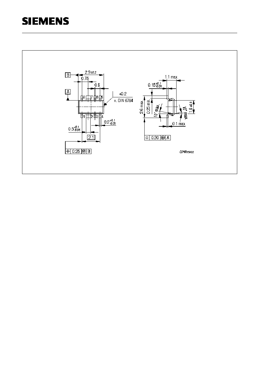
Type
Package
File
Date
CGY196
GaAs MMIC
SCT598
D:\Projekte\AKTUELL\EH_DB\lie
ferung_pdf\Lieferung\word\cgy19
26.02.1998
Key-word
Notes on Processing
Preliminary soldering recommendation
∑
Foot Print
drawing C63060-A2123-A001-01-0027
∑
Soldering
wave soldering:
unsuitable
reflow soldering:
suitable
(IR or VPR)
soldering profile:
ramp-up preheating
ramp-up peak
exposure to molten solder
typ. solder temperature
peak temperature
ramp-down
temperature gradient:
max. + 2 K/sec
time at 100 - 150 ∞C:
min. 90 sec.
temperature gradient
max. + 6 K/sec
above 183∞C
max. 150 sec
typ. 215-245∞C
max. 30 sec.
max. peak 260∞C
max. 10 sec.
temperature gradient:
min. - 6∞C/sec
(see also soldering standard profile of databook
`package information')
comments
slow ramp-up, long preheating phase and low max.
temperature recommended
∑
Solder paste thickness
150 - 200 µm
∑
Control of soldering (voids)
- visual inspection
- cross sectioning
- measurement of case temperature /
thermal resistance case to ambient
∑
Jedec A-112A
level 1
storage floor life at 30∞C/90% unlimited
∑
IPC-9501 (IPC-4202)
level 111
storage floor life at 30∞C/60% unlimited
IR/Convection; max. 245∞C; < 6K/sec.
Semiconductor Group
14
1998-11-01
CGY 196
Siemens Aktiengesellschaft
15
16.6.1998
HL HF PE GaAs
Published by Siemens AG, Bereich Halbleiter, Marketing-Kommunikation,
Balanstraþe 73, D-81541 M¸nchen.
copyright Siemens AG 1996. All Rights Reserved.
As far as patents or other rights of third parties are concerned, liability is only assumed for
components per se, not for applications, processes and cirucits implemented within
components or assemblies.
The information describes the type of component and shall not be considered as assured
characteristics.
Terms of delivery and rights to change design reserved.
For questions on technology, delivery, and prices please contact the Offices of
Semiconductor Group in Germany or the Siemens Companies and Representatives
worldwide (see address list).
Due to technical requirements components may contain dangerous substances. For
information on the type in question please contact your nearest Siemens Office,
Semiconductor Group.
Siemens AG is an approved CECC manufacturer.
Semiconductor Group
15
1998-11-01