Semiconductor Group
33
01.95
∑
1 048 576 words by 1-bit organization
∑
Fast access and cycle time
50 ns access time
95 ns cycle time (-50 version)
60 ns access time
130 ns cycle time (-60 version)
70 ns access time
130 ns cycle time (-70 version)
∑
Fast page mode cycle time
35 ns (-50 version)
40 ns (-60 version)
45 ns (-70 version)
∑
Low power dissipation
max. 495 mW active (-50 version)
max. 440 mW active (-60 version)
max. 385 mW active (-70 version)
max. 5.5 mW standby
max. 1.1 mW standby for L-version
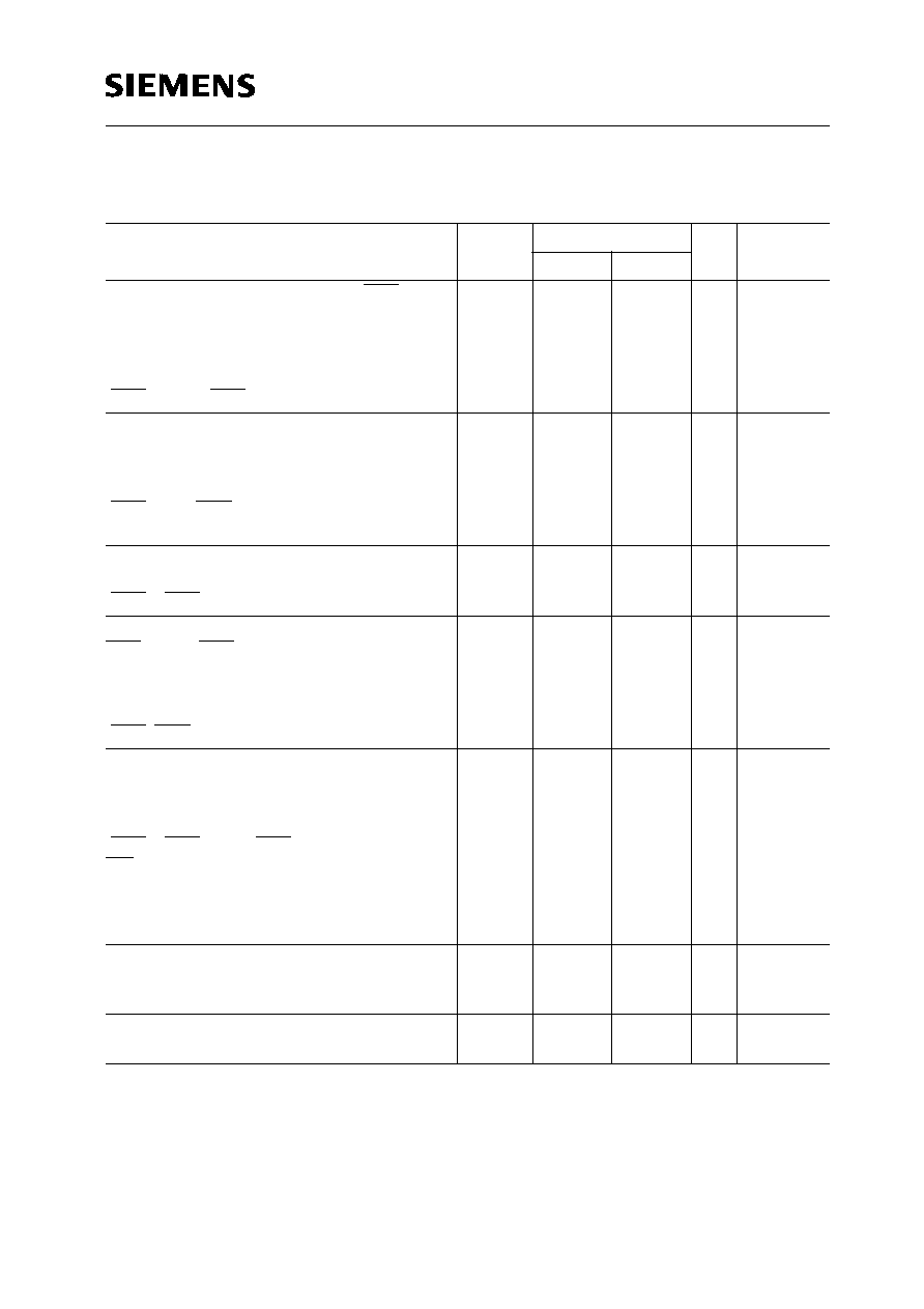
Ordering Information
Type
Ordering Code
Package
Description
HYB 511000BJ-50
Q67100-Q1056
P-SOJ-26/20-1
DRAM (access time 50 ns)
HYB 511000BJ-60
Q67100-Q518
P-SOJ-26/20-1
DRAM (access time 60 ns)
HYB 511000BJ-70
Q67100-Q519
P-SOJ-26/20-1
DRAM (access time 70 ns)
HYB 511000BJL-50
on request
P-SOJ-26/20-1
DRAM (access time 50 ns)
HYB 511000BJL-60
Q67100-Q526
P-SOJ-26/20-1
DRAM (access time 60 ns)
HYB 511000BJL-70
Q67100-Q527
P-SOJ-26/20-1
DRAM (access time 70 ns)
1 M
◊
1-Bit Dynamic RAM
Low Power 1 M
◊
1-Bit Dynamic RAM
Advanced Information
HYB 511000BJ-50/-60/-70
HYB 511000BJL-50/-60/-70
∑
Single + 5 V (
±
10 %) supply with a built-in
V
BB
generator
∑
Output unlatched at cycle end allows two-
dimensional chip selection
∑
Common I/O capability using "early write"
operation
∑
Read-modify-write, CAS-before-RAS
refresh, RAS-only refresh, hidden-refresh,
fast page mode capability and test mode
capability
∑
All inputs, outputs and clocks
TTL-compatible
∑
512 refresh cycles/8 ms
512 refresh cycles/64 ms
for L-version only
∑
Plastic Packages:
P-SOJ-26/20-1
Semiconductor Group
34
HYB 511000BJ/BJL-50/-60/-70
1 M
◊
1-DRAM
The HYB 511000BJ/BJL is the new generation dynamic RAM organized as 1 048 576 words by
1-bit. The HYB 511000BJ/BJL utilizes CMOS silicon gate process technology as well as advanced
circuit techniques to provide wide operating margins, both internally and for the system user.
Multiplexed address inputs permit the HYB 511000BJ/BJL to be packaged in a standard plastic
P-SOJ-26/20. This package size provides high system bit densities and is compatible with
commonly used automatic testing and insertion equipment. System oriented features include single
+ 5 V (
±
10 %) power supply, direct interfacing with high-performance logic device families such as
Schottky TTL. "Test Mode" function is implemented. The HYB 511000BJL are specially selected for
low power battery backup applications.
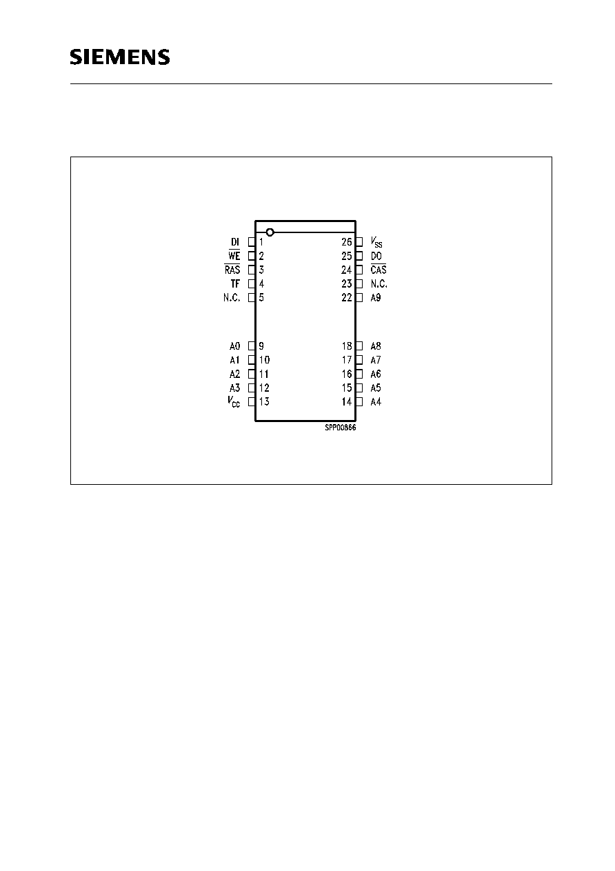
Pin Definitions and Functions
Pin No.
Function
A0-A9
Address Inputs
RAS
Row Address Strobe
DI
Data In
DO
Data Out
CAS
Column Address Strobe
WE
Read/Write Input
V
CC
Power Supply (+ 5 V)
V
SS
Ground (0 V)
TF
Test Function
N.C.
No Connection
Semiconductor Group
35
HYB 511000BJ/BJL-50/-60/-70
1 M
◊
1-DRAM
Pin Configuration
(top view)
SOJ-26/20-1

Semiconductor Group
36
HYB 511000BJ/BJL-50/-60/-70
1 M
◊
1-DRAM
Block Diagram
Semiconductor Group
37
HYB 511000BJ/BJL-50/-60/-70
1 M
◊
1-DRAM
Absolute Maximum Ratings
Operating temperature range .........................................................................................0 to + 70 ∞C
Storage temperature range......................................................................................≠ 55 to + 150 ∞C
Soldering temperature ............................................................................................................260 ∞C
Soldering time .............................................................................................................................10 s
Input/output voltage ........................................................................................................ ≠ 1 to + 7 V
Test Function Input voltage ....................................................................................... ≠ 1 to + 10.5 V
Power supply voltage...................................................................................................... ≠ 1 to + 7 V
Power dissipation..................................................................................................................... 0.6 W
Data out current (short circuit) ................................................................................................ 50 mA
Note: Stresses above those listed under "Absolute Maximum Ratings" may cause permanent
damage of the device. Exposure to absolute maximum rating conditions for extended periods
may affect device reliability.
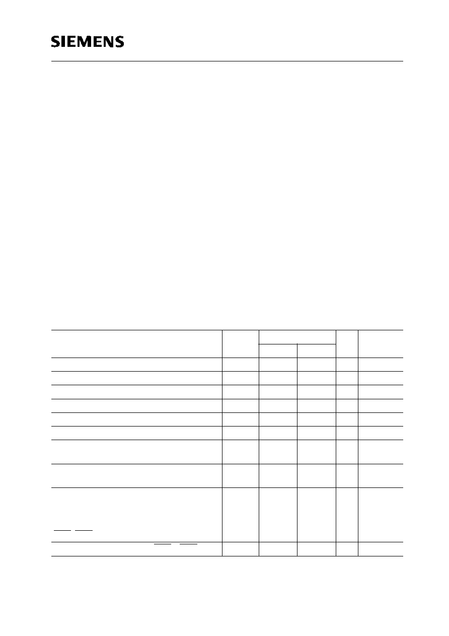
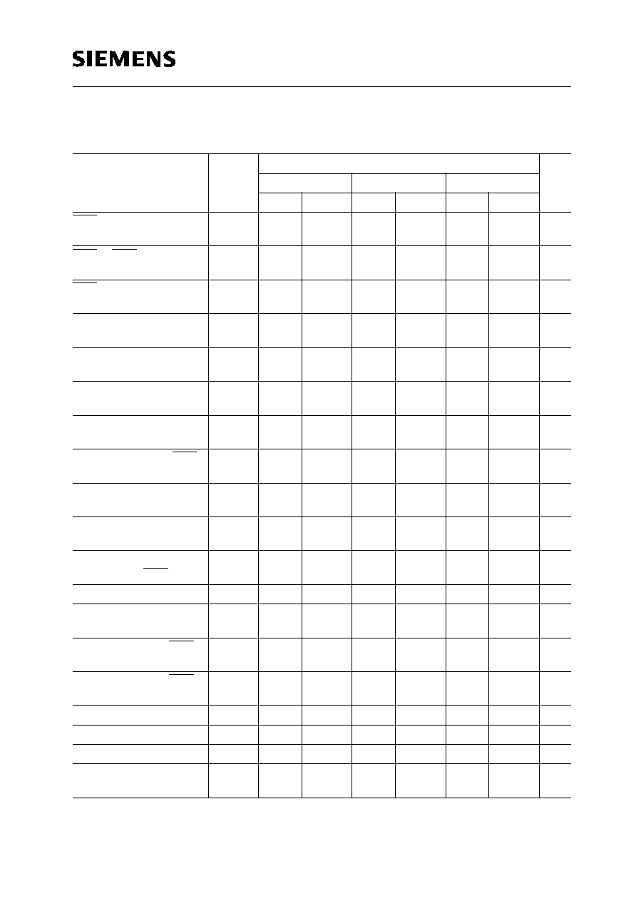
DC Characteristics
T
A
= 0 to 70 ∞C;
V
SS
= 0 V;
V
CC
= 5 V
±
10 %
Parameter
Symbol
Limit Values
Unit Test
Condition
min.
max.
Input high voltage
V
IH
2.4
6.5
V
1)
Input low voltage
V
IL
≠ 1.0
0.8
V
1)
Test enable input high voltage
V
IH(TF)
V
CC
+ 4.5 10.5
V
1)
Test disable input low voltage
V
IL(TF)
≠ 1.0
V
CC
+ 1.0 V
1)
Output high voltage (
I
OUT
= ≠ 5 mA)
V
OH
2.4
≠
V
1)
Output low voltage (
I
OUT
= 4.2 mA)
V
OL
≠
0.4
V
1)
Input leakage current, any input except TF
(0 V
V
IN
6.5 V, all other pins = 0 V)
I
I(L)
≠ 10
10
µ
A
1)
Output leakage current
(DO is disabled, 0 V
V
OUT
5.5 V)
I
O(L)
≠ 10
10
µ
A
1)
Average
V
CC
supply current:
-50 version
-60 version
-70 version
(RAS, CAS, address cycling:
t
RC
=
t
RC
min.)
I
CC1
≠
≠
≠
90
80
70
mA
mA
mA
2) 3)
2) 3)
2) 3)
Standby
V
CC
supply current (RAS = CAS =
V
IH
)
I
CC2
≠
2
mA
≠
Semiconductor Group
38
HYB 511000BJ/BJL-50/-60/-70
1 M
◊
1-DRAM
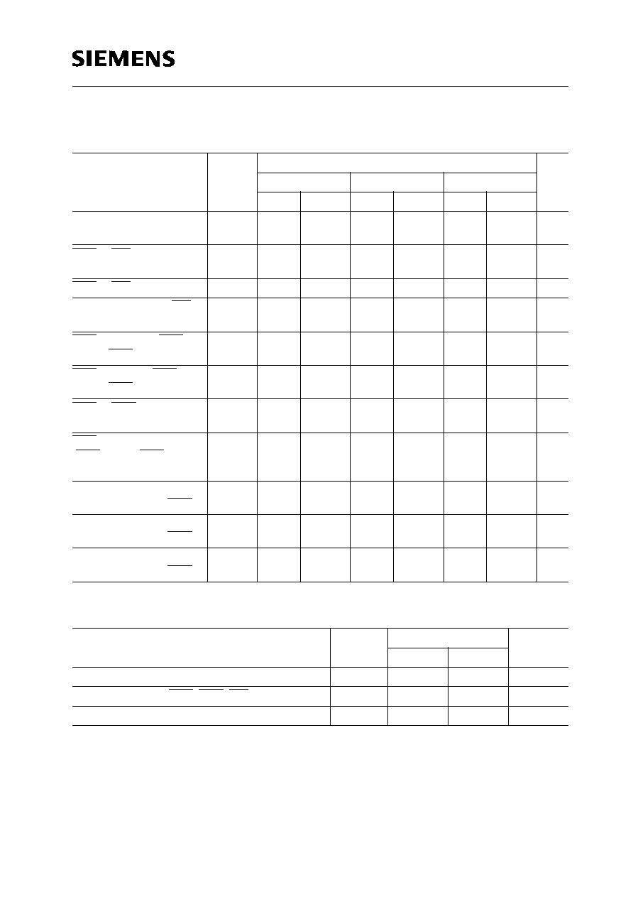
Average
V
CC
supply current during RAS only
refresh cycles:
-50 version
-60 version
-70 version
(RAS cycling: CAS =
V
IH
:
t
RC
=
t
RC
min.)
I
CC3
≠
≠
≠
90
80
70
mA
mA
mA
2)
2)
2)
Average
V
CC
supply current during fast page
modes:
-50 version
-60 version
-70 version
(RAS =
V
IL
, CAS, address cycling:
t
PC
=
t
PC
min.)
I
CC4
≠
≠
≠
70
60
50
mA
mA
mA
2) 3)
2) 3)
2) 3)
Standby
V
CC
supply current
L-Version
(RAS = CAS =
V
CC
≠ 0.2 V)
I
CC5
≠
≠
1
200
mA
µ
A
1)
1)
Average
V
CC
supply current during
CAS-before-RAS refresh mode:
-50 version
-60 version
-70 version
(RAS, CAS, address cycling:
t
RC
=
t
RC
min.)
I
CC6
≠
≠
≠
90
80
70
mA
mA
mA
2)
2)
2)
For L-version only:
Battery backup current:
average power supply current, battery backup
mode:
(CAS = CAS before RAS cycling or 0.2 V,
WE =
V
CC
≠ 0.2 V or 0.2 V,
A0 to A9 =
V
CC
≠ 0.2 V or 0.2 V,
DI =
V
CC
≠ 0.2 V or 0.2 V open,
t
RC
= 125
µ
s,
t
RAS
=
t
RAS
min. ~ 1
µ
s)
I
CC7
≠
300
µ
A
2)
Input leakage current (only TF)
(0 V
V
IN
(TF)
V
CC
+ 0.5 V)
All other pins not under test = 0 V
I
ITF(L)
≠ 10
+ 10
µ
A
1)
Test function input current
(
V
CC
+ 4.5
V
IN
(TF)
10.5 V)
I
TF
≠
1
mA
1)
DC Characteristics (cont'd)
T
A
= 0 to 70 ∞C;
V
SS
= 0 V;
V
CC
= 5 V
±
10 %
Parameter
Symbol
Limit Values
Unit Test
Condition
min.
max.

Semiconductor Group
39
HYB 511000BJ/BJL-50/-60/-70
1 M
◊
1-DRAM
AC Characteristics
4) 13)
T
A
= 0 to 70 ∞C;
V
CC
= 5 V
±
10 %;
t
T
= 5 ns
Parameter
Symbol
Limit Values
Unit
-50
-60
-70
min.
max.
min.
max.
min.
max.
Random read or write
cycle time
t
RC
95
≠
110
≠
130
≠
ns
Read-write cycle time
t
RWC
115
≠
130
≠
155
≠
ns
Fast page mode cycle
time
t
PC
35
≠
40
≠
45
≠
ns
Fast page mode read-
write cycle time
t
PRWC
55
≠
60
≠
70
≠
ns
Access time from
RAS
6) 11)
t
RAC
≠
50
≠
60
≠
70
ns
Access time from
CAS
6) 11)
t
CAC
≠
15
≠
15
≠
20
ns
Access time from column
address
6) 12)
t
AA
≠
25
≠
30
≠
35
ns
Access time from CAS
precharge
6)
t
CPA
≠
30
≠
35
≠
40
ns
CAS to output in low-Z
6)
t
CLZ
0
≠
0
≠
0
≠
ns
Output buffer turn-off
delay
7)
t
OFF
0
15
0
20
0
20
ns
Transition time
(rise and fall)
5)
t
T
3
50
3
50
3
50
ns
RAS precharge time
t
RP
35
≠
40
≠
50
≠
ns
RAS pulse width
t
RAS
50
10.000
60
10.000
70
10.000
ns
RAS pulse width (fast
page mode)
t
RASP
50
100.000 60
100.000 70
100.000 ns
RAS hold time
t
RSH
15
≠
15
≠
20
≠
ns
CAS hold time
t
CSH
50
≠
60
≠
70
≠
ns
RAS hold time from CAS
precharge (FPM)
t
RHCP
30
≠
35
≠
45
≠
ns
CAS precharge to WE
delay time (FPM RMW)
t
CPWD
30
≠
35
≠
45
≠
ns
CAS pulse width
t
CAS
15
10.000
15
10.000
20
10.000
ns
RAS to CAS delay
time
11)
t
RCD
20
35
20
45
20
50
ns
Semiconductor Group
40
HYB 511000BJ/BJL-50/-60/-70
1 M
◊
1-DRAM
RAS to column address
delay time
12)
t
RAD
15
25
15
30
15
35
ns
CAS to RAS precharge
time
t
CRP
5
≠
5
≠
5
≠
ns
CAS precharge time (fast
page mode)
t
CP
10
≠
10
≠
10
≠
ns
Row address
setup time
t
ASR
0
≠
0
≠
0
≠
ns
Row address
hold time
t
RAH
10
≠
10
≠
10
≠
ns
Column address setup
time
t
ASC
0
≠
0
≠
0
≠
ns
Column address hold
time
t
CAH
15
≠
15
≠
15
≠
ns
Column address to RAS
lead time
t
RAL
25
≠
30
≠
35
≠
ns
Read command setup
time
t
RCS
0
≠
0
≠
0
≠
ns
Read command hold
time
8)
t
RCH
0
≠
0
≠
0
≠
ns
Read command hold time
referenced to RAS
8)
t
RRH
0
≠
0
≠
0
≠
ns
Write command hold time
t
WCH
10
≠
10
≠
15
≠
ns
Write command pulse
width
t
WP
10
≠
10
≠
15
≠
ns
Write command to RAS
lead time
t
RWL
15
≠
15
≠
20
≠
ns
Write command to CAS
lead time
t
CWL
15
≠
15
≠
20
≠
ns
Data setup time
9)
t
DS
0
≠
0
≠
0
≠
ns
Data hold time
9)
t
DH
10
≠
15
≠
15
≠
ns
Refresh period
t
REF
≠
8
≠
8
≠
8
ms
Refresh period for
L-version only
t
REF
≠
64
≠
64
≠
64
ms
AC Characteristics (cont'd)
4) 13)
T
A
= 0 to 70 ∞C;
V
CC
= 5 V
±
10 %;
t
T
= 5 ns
Parameter
Symbol
Limit Values
Unit
-50
-60
-70
min.
max.
min.
max.
min.
max.
Semiconductor Group
41
HYB 511000BJ/BJL-50/-60/-70
1 M
◊
1-DRAM
Write command setup
time
10)
t
WCS
0
≠
0
≠
0
≠
ns
CAS to WE delay
time
10)
t
CWD
15
≠
15
≠
20
≠
ns
RAS to WE delay time
10)
t
RWD
50
≠
60
≠
70
≠
ns
Column address to WE
delay time
10)
t
AWD
25
≠
30
≠
35
≠
ns
CAS setup time (CAS-
before-RAS cycle)
t
CSR
5
≠
5
≠
5
≠
ns
CAS hold time (CAS-
before-RAS cycle)
t
CHR
10
≠
15
≠
15
≠
ns
RAS to CAS precharge
time
t
RPC
0
≠
0
≠
0
≠
ns
CAS precharge time
(CAS-before-RAS
counter test cycle)
t
CPT
25
≠
30
≠
40
≠
ns
Test mode enable setup
time referenced to RAS
t
TES
0
≠
0
≠
0
≠
ns
Test mode enable hold
time referenced to RAS
t
TEHR
0
≠
0
≠
0
≠
ns
Test mode enable hold
time referenced to CAS
t
TEHC
0
≠
0
≠
0
≠
ns
Capacitance
T
A
= 0 to 70 ∞C;
V
CC
= 5 V
±
10 %;
f
= 1 MHz
Parameter
Symbol
Limit Values
Unit
min.
max.
Input capacitance (A0 to A9, DI)
C
I1
≠
5
pF
Input capacitance (RAS, CAS, WE, TF)
C
I2
≠
7
pF
Output capacitance (DO)
C
O
≠
7
pF
AC Characteristics (cont'd)
4) 13)
T
A
= 0 to 70 ∞C;
V
CC
= 5 V
±
10 %;
t
T
= 5 ns
Parameter
Symbol
Limit Values
Unit
-50
-60
-70
min.
max.
min.
max.
min.
max.
Semiconductor Group
42
HYB 511000BJ/BJL-50/-60/-70
1 M
◊
1-DRAM
Notes :
1) All voltages are referenced to
V
SS
.
2)
I
CC1
,
I
CC3
,
I
CC4
,
I
CC6
,
I
CC7
depend on cycle rate.
3)
I
CC1
and
I
CC4
depend on output loading. Specified values are measured with the output open.
4) An initial pause of 200
µ
s is required after power-up followed by 8 RAS cycles before proper device operation
is achieved. In case of using internal refresh counter, a minimum of 8 CAS-before-RAS initialization cycles
instead of 8 RAS cycles are required.
5)
V
IH
(min.) and
V
IL
(max.) are reference levels for measuring timing of input signals. Transition times are also
measured between
V
IH
and
V
IL
.
6) Measured with a load equivalent to 2 TTL loads and 100 pF.
7)
t
OFF
(max.) defines the time at which the output achieves the open-circuit conditions and is not referenced to
output voltage levels.
8) Either
t
RCH
or
t
RRH
must be satisfied for a read cycle.
9) These parameters are referenced to the CAS leading edge in early write cycles and to the WE leading edge
in read-write cycles.
10)
t
WCS
,
t
RWD
,
t
CWD
and
t
AWD
are not restrictive operating parameters. They are included in the data sheet as
electrical characteristics only.
If
t
WCS
t
WCS
(min.), the cycle is an early write cycle and data out pin will remain open-circuit (high impedance)
through the entire cycle; if
t
RWD
t
RWD
(min.),
t
CWD
t
CWD
(min.) and
t
AWD
t
AWD
(min.), the cycle is a read-write
cycle and DO will contain data read from the selected cell. If neither of the above sets of conditions is satisfied,
the condition of DO (at access time) is indeterminate.
11) Operation within the
t
RCD
(max.) limit insures that
t
RAC
(max.) can be met.
t
RCD
(max.) is specified as a reference
point only. If
t
RCD
is greater than the specified
t
RCD
(max.) limit, then access time is controlled by
t
CAC
.
12) Operation within the
t
RAD
(max.) limit insures that
t
RAC
(max.) can be met.
t
RAD
(max.) is specified as a reference
point only. If
t
RAD
is greater than the specified
t
RAD
(max.) limit, then access time is controlled by
t
AA
.
13) AC measurements assume
t
T
= 5ns.
Semiconductor Group
43
HYB 511000BJ/BJL-50/-60/-70
1 M
◊
1-DRAM
Waveforms
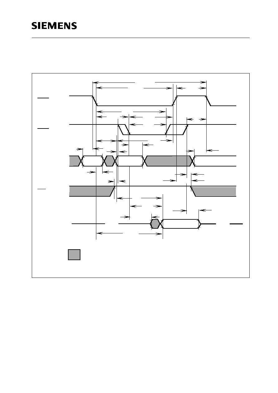
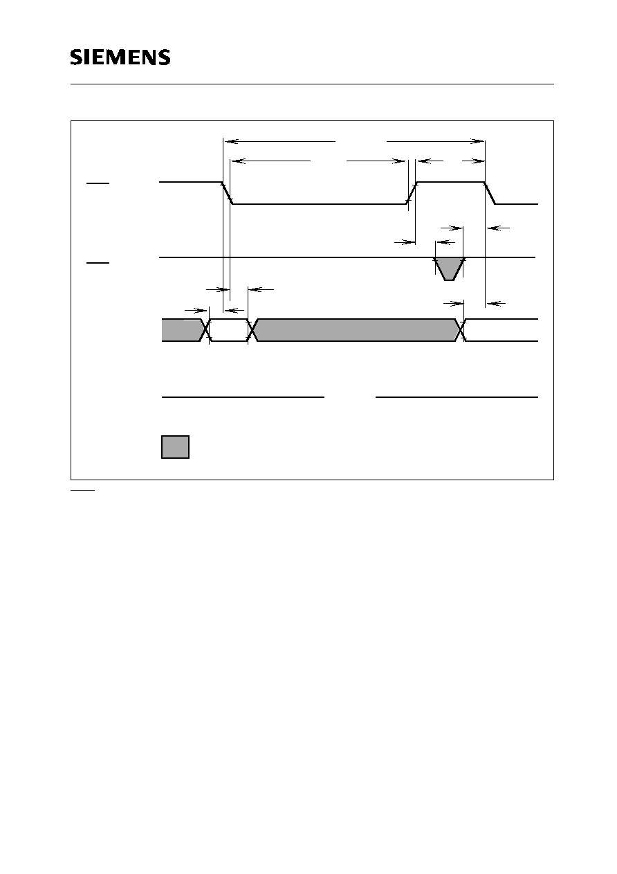
Read Cycle
Row
Address
Column
Address
Row
Address
Valid Data Out
RAS
CAS
A0 - A9
WE
DO
(Output)
V
IH
V
IL
V
IH
V
IL
V
IH
V
IL
V
IH
V
IL
V
OH
VOL
t
RAS
t
RC
t
CSH
t
RAD
t
CAS
t
RP
t
RAH
t
CRP
t
RSH
t
RCD
t
RAL
t
ASR
t
CAH
t
ASC
t
ASR
t
RCH
t
RRH
t
RCS
t
AA
t
CLZ
t
CAC
t
OFF
t
RAC
Hi Z
Hi Z
"H" or "L"
Semiconductor Group
44
HYB 511000BJ/BJL-50/-60/-70
1 M
◊
1-DRAM
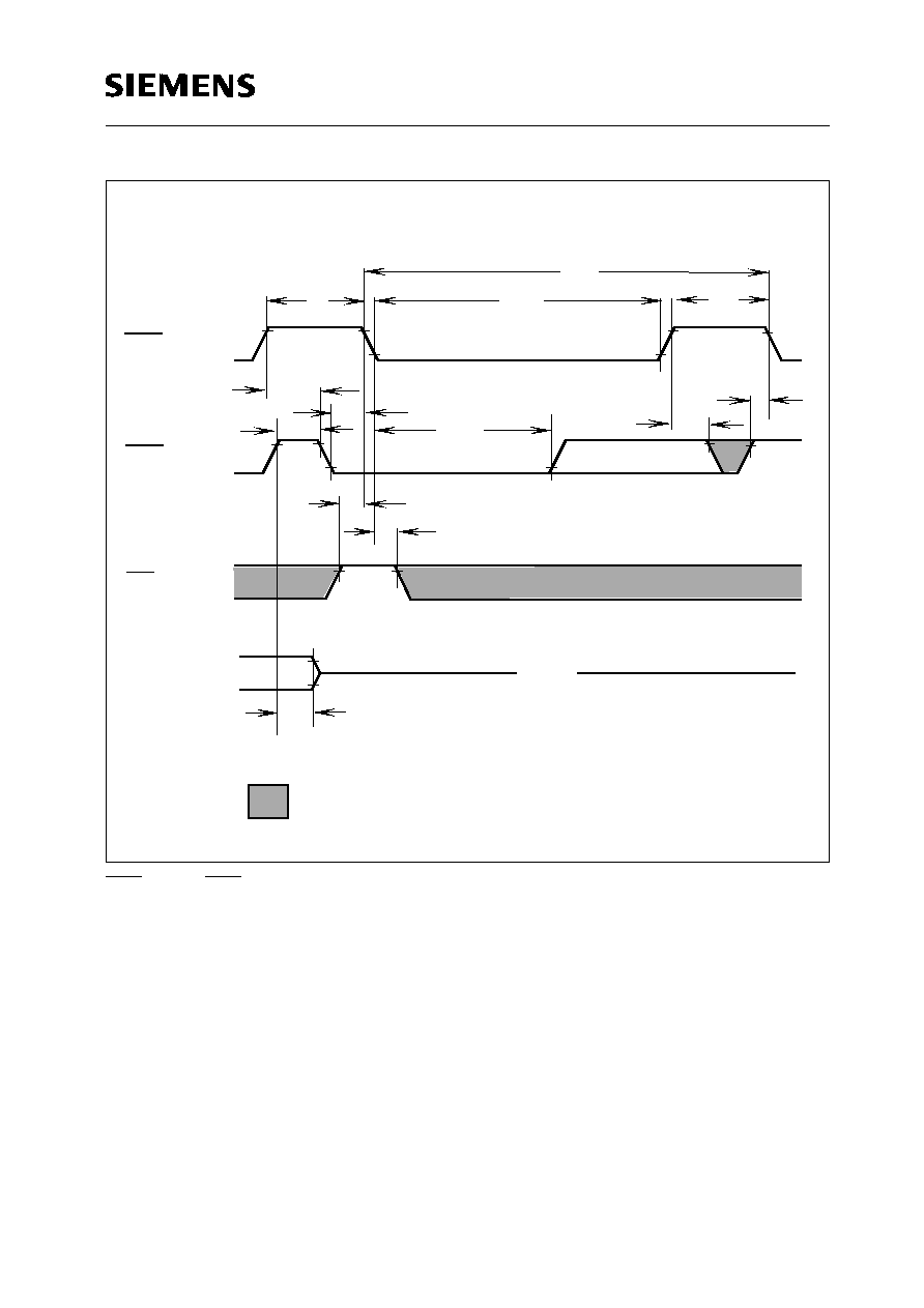
Write Cycle (Early Write)
RAS
CAS
A0 - A9
WE
V
IH
V
IL
V
IH
V
IL
V
IH
V
IL
V
IH
V
IL
.
t
RAS
t
RC
t
CSH
t
RAD
t
CAS
t
RP
t
CRP
t
RSH
t
RCD
t
RAL
t
ASR
t
CAH
t
ASR
(Input)
(Output)
t
CWL
t
RWL
t
WP
t
ASC
t
WCH
Valid Data In
t
DS
t
DH
Hi Z
Column
Address
Address
Row
Row
Address
t
RAH
t
WCS
"H" or "L"
DI
V
IH
V
IL
DO
V
OH
V
OL
Semiconductor Group
45
HYB 511000BJ/BJL-50/-60/-70
1 M
◊
1-DRAM
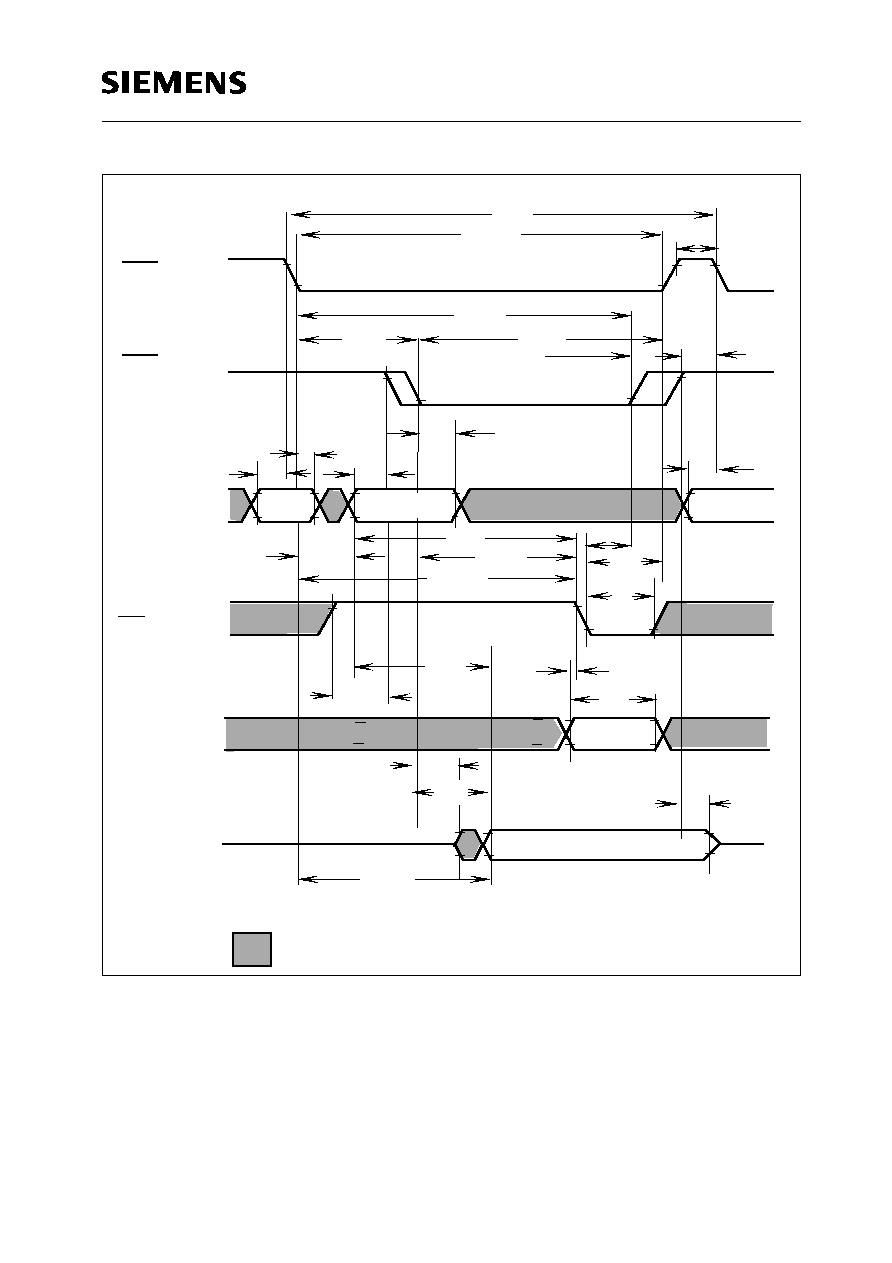
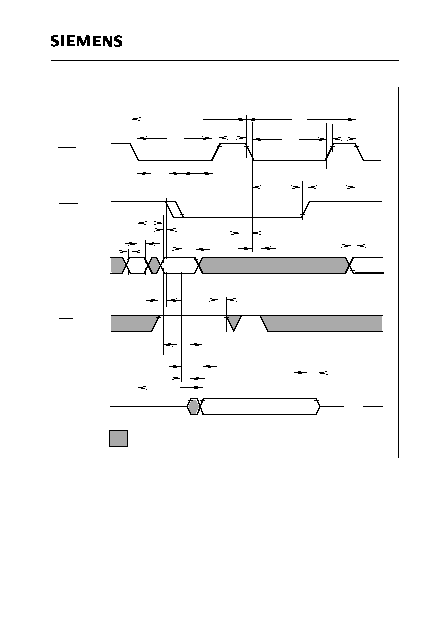
Read-Write (Read-Modify-Write) Cycle
Row
Address
Row
Address
t
CSH
t
CAS
t
CRP
t
RWC
t
AWD
t
ASR
t
RP
t
RAS
t
RAH
t
CAH
DO
(Output)
V
OH
V
OL
V
IH
V
IL
DI
(Input)
WE
V
IH
V
IL
t
ASR
Column
Address
t
RCD
t
DH
t
RSH
t
RAD
t
CWD
t
RWD
t
RWL
t
CWL
t
CLZ
t
WP
t
RCS
t
DS
t
CAC
t
OFF
Valid
Data in
Data Out
"H" or "L"
t
ASC
V
IH
V
IL
V
IH
V
IL
t
RAC
t
AA
RAS
CAS
A0 - A9
Semiconductor Group
46
HYB 511000BJ/BJL-50/-60/-70
1 M
◊
1-DRAM
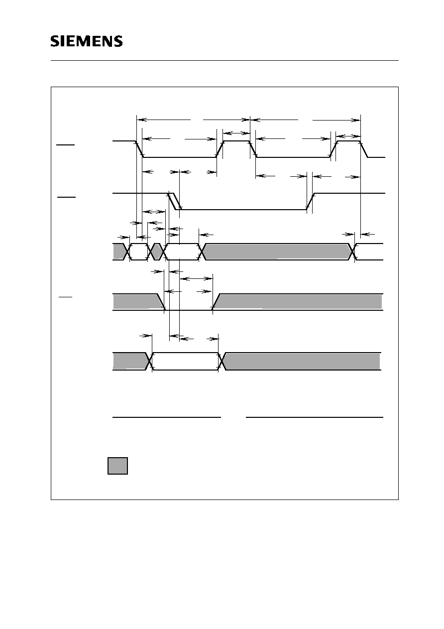
Fast Page Mode Read-Modify-Write Cycle
t
CAH
t
CP
t
RAC
t
CAC
t
CLZ
t
RCS
t
AA
t
RCD
t
RAD
t
RAH
t
ASR
t
ASC
t
CAS
t
CAS
t
PRWC
t
CWD
t
CAH
t
ASC
t
CAS
t
RSH
t
RP
t
CRP
t
ASR
t
CAH
t
ASC
t
RAL
t
CWD
t
RWD
t
CWL
t
CWL
t
CWD
t
AWD
t
AWD
t
WP
t
WP
t
CWL
t
RWL
t
AWD
t
WP
t
DH
t
DS
t
CPA
t
CLZ
t
AA
t
CAC
t
DS
t
DH
t
AA
t
CPA
t
CLZ
t
DS
t
DH
RAS
V
IH
V
IL
CAS
V
IH
V
IL
V
IH
V
IL
V
IH
V
IL
V
IH
V
IL
V
OH
V OL
WE
DI (Input)
DO
(Output)
Data In
Data In
Data In
Out
Data
Data
Out
Address
Row
Column
Address
Address
Column
Address
Row
Address
t
RASP
t
CSH
Column
t
CPWD
t
CPWD
"H" or "L"
A0-A9
t
OFF
t
OFF
t
OFF
Data
Out

Semiconductor Group
47
HYB 511000BJ/BJL-50/-60/-70
1 M
◊
1-DRAM
Fast Page Mode Read Cycle
t
RASP
t
CAS
t
CAS
t
PC
t
CP
t
RCD
t
CSH
t
CAH
t
CAH
t
ASC
t
ASC
t
ASR
t
RAH
t
RAD
t
RCS
t
RCS
t
RCS
t
ASC
t
CAH
t
CAS
t
RSH
t
CRP
t
RP
t
ASR
t
RCH
t
CPA
t
AA
t
AA
t
RRH
t
CPA
t
AA
t
OFF
t
OFF
t
CAC
t
CAC
t
CLZ
t
CLZ
t
CLZ
t
OFF
t
RAC
t
CAC
Valid
Data Out
Data Out
Data Out
Valid
Valid
Column
Address
Address
Addr
Address
Column
Row
Row
RAS
DO
(Output)
WE
A0-A9
CAS
V
IH
V
IL
V
IH
V
IL
V
IH
V
IL
V
IH
V
IL
"H" or "L"
t
RHCP
t
RCH
V
OH
V
OL
Column
Address

Semiconductor Group
48
HYB 511000BJ/BJL-50/-60/-70
1 M
◊
1-DRAM
Fast Page Mode Early Write Cycle
t
RASP
t
RP
t
RSH
t
CAS
t
CAS
t
CP
t
CRP
t
RAL
t
CAH
t
ASR
t
CWL
t
RWL
t
CAH
t
ASC
t
ASC
t
CWL
t
CWL
t
WCS
t
WCS
t
WCS
t
WCH
t
WP
t
WP
t
WCH
t
WP
t
WCH
t
RAD
t
CAS
t
RCD
t
PC
t
CAH
t
RAH
t
ASR
t
ASC
t
DH
t
DS
t
DS
t
DH
t
DH
t
DS
Column
Address
Address
Address
Column
Row
Row
Addr
Valid
Data In
Valid
Valid
Data In
Data In
Column
Address
HI-Z
RAS
DO
(Output)
DI
(Input)
WE
A0-A9
CAS
V
IH
V
IL
V
IH
V
IL
V
IH
V
IL
V
IH
V
IL
V
IH
V
IL
"H" or "L"
V
OH
V
OL
Semiconductor Group
49
HYB 511000BJ/BJL-50/-60/-70
1 M
◊
1-DRAM
RAS-Only Refresh Cycle
t
CRP
t
RAH
t
RP
t
RAS
t
RC
t
ASR
t
ASR
t
RPC
V
IH
V
IL
V
IH
V
IL
V
IH
V
IL
V
OH
V
OL
Row
Address
Row
Address
HI-Z
A0-A9
RAS
CAS
DO
(Output)
"H" or "L"
Semiconductor Group
50
HYB 511000BJ/BJL-50/-60/-70
1 M
◊
1-DRAM
CAS-Before-RAS Refresh Cycle
t
RP
t
RAS
t
RP
t
RC
t
CRP
t
CP
t
RPC
t
CHR
t
WRH
t
WRP
t
CSR
t
RPC
t
OFF
V
IH
V
IL
V
IH
V
IL
V
IH
V
IL
HI-Z
"H" or "L"
RAS
DO
(Output)
WE
CAS
V
OH
V
OL
Semiconductor Group
51
HYB 511000BJ/BJL-50/-60/-70
1 M
◊
1-DRAM
Hidden Refresh Cycle (Read)
RAS
DO
(Output)
WE
A0-A9
CAS
t
RC
t
RC
t
RAS
t
RAS
t
RP
t
RP
t
CRP
t
CHR
t
RAD
t
CAH
t
ASC
t
RAH
t
ASR
t
ASR
t
RCS
t
RRH
t
AA
t
CAC
t
RAC
t
CLZ
t
OFF
t
RCD
t
RSH
V
IH
V
IL
V
IH
V
IL
V
IH
V
IL
V
IH
V
IL
t
WRP
t
WRH
"H" or "L"
Valid Data Out
Row
Address
Column
Address
Row
Addr
HI-Z
V
OH
V
OL
Semiconductor Group
52
HYB 511000BJ/BJL-50/-60/-70
1 M
◊
1-DRAM
Hidden Refresh Cycle (Early Write)
RAS
DO
(Output)
DI
(Input)
WE
A0-A9
V
IH
V
IL
V
IH
V
IL
V
IH
V
IL
CAS
V
IH
V
IL
V
IH
V
IL
"H" or "L"
t
RC
t
RAS
t
RCD
t
RSH
t
RAD
t
CAH
t
WCS
t
WCH
t
WP
t
ASR
t
RAH
t
DS
t
DH
t
ASR
t
CRP
t
CHR
t
RP
t
RAS
t
RC
t
RP
t
ASC
Address
Row
Addr
Row
Address
Valid Data
HI-Z
Column
V
OH
V
OL
Semiconductor Group
53
HYB 511000BJ/BJL-50/-60/-70
1 M
◊
1-DRAM
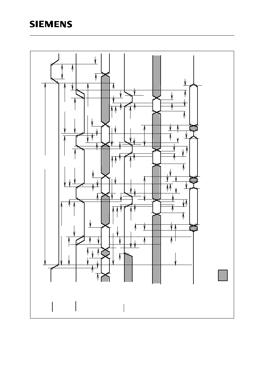
CAS-Before-RAS Refresh Counter Test Cycle
Valid
"H" or "L"
t
CSR
t
ASR
t
ASC
t
CHR
t
CPT
t
WRP
t
RAL
t
CAH
t
RSH
t
RP
t
RAS
t
CAS
t
RCS
t
CAC
t
AA
t
WRH
t
CLZ
t
RWL
t
CWL
t
WCH
t
WCS
t
WRH
t
WRP
t
DS
t
OFF
t
DH
t
WRH
t
WRP
t
RWL
t
CWL
t
AWD
t
CWD
t
WP
t
RCS
t
CAC
t
AA
t
DH
t
DS
t
CAC
V
IH
V
IL
V
IH
V
IL
V
IH
V
IL
V
IH
V
IL
V
OH
V
OL
V
OH
V
OL
V
IH
V
IL
V
IH
V
IL
V
IH
V
IL
V
IH
V
IL
V
IH
V
IL
DI
(Input)
RAS
WE
A0-A9
CAS
DO
(Output)
DO
(Output)
DI
(Input)
WE
WE
DO
(Output)
Column
Address
Row
Address
Data In
Valid Data Out
Data In
HI-Z
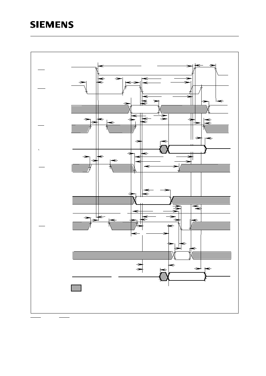
Read Cycle
Read-Modify-Write Cycle
Write Cycle
t
RRH
t
RCH
t
OFF
Valid Data Out
HI-Z
HI-Z
CLZ
t
Semiconductor Group
54
HYB 511000BJ/BJL-50/-60/-70
1 M
◊
1-DRAM
Test Mode
The HYB 511000B/BL is the RAM organized 1 048 576 words by 1-bit, it is internally organized
262 144 words by 4-bit. In "Test Mode", data would be written into a number of sectors (4 sectors)
in parallel and retrieved the same way. If upon reading, all bits are equal (all "H" or "L"), the data
output pin indicates a same data as all bits. In this case, the data output pin indicates an expected
data for good parts, the data output pin indicates a complementary data for bad parts. And also, if
any of the bits differed, the data output pin would indicate a high impedance state for bad parts. The
next figure shows the block diagram including its truth table when "Test Mode" is used.
In test mode, 1M DRAM can be tested as if it were 256K DRAM by the following method.
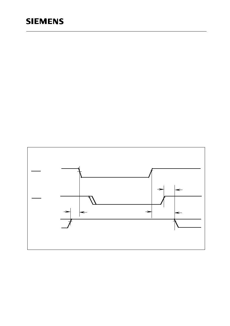
"Test Mode" function is performed on any of the timing cycles including fast page mode when "TF"
pin is held on "super voltage (
V
CC
+ 4.5 V (
V
CC
= 5 V
±
10 %), max. voltage = 10.5 V)" for the
specified period (
t
TES
,
t
TEHR
and
t
TEHC
; see next figure). The address input of A9 is ignored in the
"Test Mode". On the other hand, normal operation requires the "TF" pin be connected to
V
IL
(TF)
level, or left unconnected on the printed wiring board. The "Test Mode" function reduces test times
(1/4; in case of using N test pattern).
RAS
CAS
V
IH
V
IL
V
IH
V
IL
t
TEHC
TF
V
IH,TF
V
IL,TF
t
TES
t
TEHR
Test Mode Cycle