 | –≠–ª–µ–∫—Ç—Ä–æ–Ω–Ω—ã–π –∫–æ–º–ø–æ–Ω–µ–Ω—Ç: Q62702G62 | –°–∫–∞—á–∞—Ç—å:  PDF PDF  ZIP ZIP |
CGY 184
Siemens Aktiengesellschaft
1
23.07.97
HL HF PE GaAs
GaAs MMIC
Preliminary Data
l
Power amplifier for PCN applications
l
2.5 W (34dBm) output power at 3.5 V
l
Overall power added efficiency 43 %
l
Fully integrated 4 stage amplifier
l
Power ramp control
l
Input matched to 50 ohms, simple output match
ESD: Electrostatic discharge sensitive device,
observe handling precautions!
Type
Marking
Ordering code
(taped)
Package
1)
CGY 184
CGY 184
Q62702G62
MW 16
Maximum ratings
Characteristics
Symbol
max. Value
Unit
Positive supply voltage
VD
9
V
Supply current
ID
4
A
Channel temperature
TCh
150
∞C
Storage temperature
Tstg
-55...+150
∞C
Pulse peak power dissipation
duty cycle 12.5%, ton=0.577ms
PPulse
tbd
W
Total power dissipation (Tc
&�
Tc: Temperature on case
Ptot
8.5
W
Thermal Resistance
Characteristics
Symbol
max. Value
Unit
Junction-Case
2)
RthJC
8.5
K/W
1)
Dimensions see page 14
2)
see also page 9
Semiconductor Group
1
1998-11-01

CGY 184
Siemens Aktiengesellschaft
2
23.07.97
HL HF PE GaAs
Functional block diagram
Pin #
Configuration
1
n. c.
2
Vcon
Control voltage for power ramping
3
P
IN
RF-input
4
V
D1
Drain voltage 1st stage
5
Gnd1
Ground pin 1st stage
6
Gnd2
Ground pin 2nd stage
7
V
D2
Drain voltage 2nd stage
8
V
D3
Drain voltage 3rd stage
9,10,11
P
OUT
/V
D4
Drain voltage 4th stage and RF-output
12
n. c.
13
n. c.
14
n. c.
15
V
neg
Block capacitor negativ voltage generator
16
n. c.
(17)
GND3
Ground (backside of MW16 housing)
VD2(7)
Pout/VD4 (9,10,11
VD1(4)
Vc
on
(2
)
Vneg(15)
Pin(3)
control circuit
GND1(5)
VD3(8)
GND3(17)
GND2(6)
Semiconductor Group
2
1998-11-01

CGY 184
Siemens Aktiengesellschaft
3
23.07.97
HL HF PE GaAs
Electrical characteristics
(TA = 25∞C , f=1.75 GHz, ZS=ZL=50 Ohm, VD=3.5V, Vaux=3.5V, Vcontrol=2.5V, unless
otherwise specified; pulsed with a duty cycle of 12.5%, ton=577usec)
Characteristics
Symbol
min
typ
max
Unit
Supply current
V
D
=3.5V; P
in
=0dBm
IDD
-
1.67
-
A
Supply current neg. voltage gener.
V
aux
=3.5V
Iaux
-
10
-
mA
Control Current
I
C
2
3
mA
Shut-off current
( Vc=0V, V
D
=3.5V, no RF- drive )
I
D
40
µ
A
Small signal gain
P
in
=-10dBm
G
-
40
-
dB
Power gain
V
D
=3.5V; Pin=0dBm
G
-
34
-
dB
Output Power
V
D
=3.5V; Pin=0dBm
Po
-
34
-
dBm
Power gain
V
D
=3.5V; P
in
=0dBm, T=85∞C
G
-
33.7
-
dB
Output Power
V
D
=3.5V; Pin=0dBm, T=85∞C
Po
-
33.7
-
dBm
Overall Power added Efficiency
V
D
=3.5V; ; V
C
=2.5V; Pin=0dBm
-
43
-
%
Dynamic range (P
out,max
-P
out,min
)
V
C
= 0.5....2.5V
-
80
-
dB
Harmonics
2f
0
V
C
=2.2V, P
in
=0dBm
3f
0
-
-
-60
-40
-
-
dBc
RX-Noise Power
V
C
=2.2V; P
in
=0dBm ;
f
RX
=1.805....1.88GHz
-
-80
-
dBm/
100kHz
Input VSWR
V
D
=3.5V
-
-
1.8 : 1
-
-
Semiconductor Group
3
1998-11-01
CGY 184
Siemens Aktiengesellschaft
4
23.07.97
HL HF PE GaAs
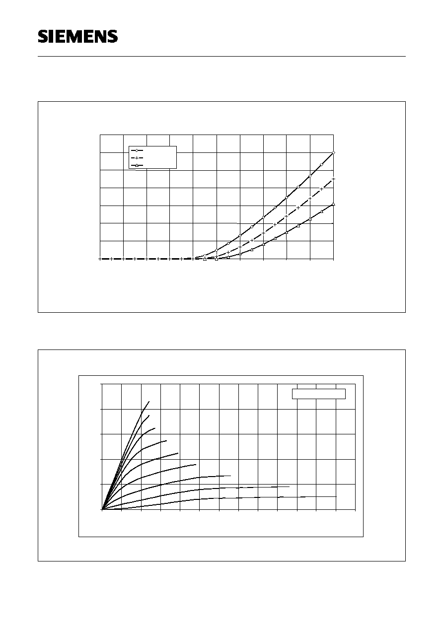
DC-ID(Vneg) characteristics ≠ typical values of stage 1 and 2, V
D
=3V
DC-Output characteristics ≠ typical values of stage 1 and 2
Pin 2( Vcon ) has to be open during measuring DC-characteristics
0
0,05
0,1
0,15
0,2
0,25
0,3
0,35
-5
-4,5
-4
-3,5
-3
-2,5
-2
-1,5
-1
-0,5
0
Vneg [V]
ID
[A]
High current
Medium current
Low current
0
0,05
0,1
0,15
0,2
0,25
0
0,5
1
1,5
2
2,5
3
3,5
4
4,5
5
5,5
6
6,5
VD [V]
ID
[
A
]
Vneg=-0.25
-0.50 V
-1.50 V
-1.25 V
-1.00 V
-0.75 V
-2.00 V
-1.75 V
-2.25 V
Ptot=223.7m W
Semiconductor Group
4
1998-11-01
CGY 184
Siemens Aktiengesellschaft
5
23.07.97
HL HF PE GaAs
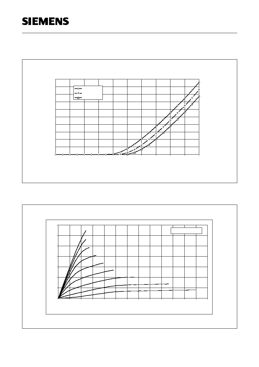
DC-ID(Vneg) characteristics ≠ typical values of stage 3, VD=3V
DC-Output characteristics ≠ typical values of stage 3
Pin 2( Vcon ) has to be open during measuring DC-characteristics
0
0,2
0,4
0,6
0,8
1
1,2
1,4
1,6
1,8
2
-5
-4,5
-4
-3,5
-3
-2,5
-2
-1,5
-1
-0,5
0
Vneg [V]
ID
[A]
High current
Medium current
Low current
0
0,2
0,4
0,6
0,8
1
1,2
1,4
0
0,5
1
1,5
2
2,5
3
3,5
4
4,5
5
5,5
6
6,5
VD [V]
ID
[
A
]
Vneg=-0.25
-0.50 V
-1.50 V
-1.25 V
-1.00 V
-0.75 V
-2.00 V
-1.75 V
-2.25 V
Ptot=1.34 W
Semiconductor Group
5
1998-11-01
CGY 184
Siemens Aktiengesellschaft
6
23.07.97
HL HF PE GaAs
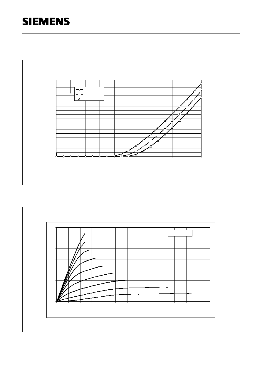
DC-ID(Vneg) characteristics ≠ typical values of stage 4, VD=3V
DC-Output characteristics ≠ typical values of stage 4
Pin 2( Vcon ) has to be open during measuring DC-characteristics
0
0,5
1
1,5
2
2,5
3
3,5
4
4,5
5
5,5
6
6,5
7
7,5
8
8,5
9
9,5
10
-5
-4,5
-4
-3,5
-3
-2,5
-2
-1,5
-1
-0,5
0
Vneg [V]
ID
[A]
High current
Medium current
Low current
0
1
2
3
4
5
6
7
0
0,5
1
1,5
2
2,5
3
3,5
4
4,5
5
5,5
6
6,5
VD [V]
ID
[
A
]
Vneg=-0.25
-0.50 V
-1.50 V
-1.25 V
-1.00 V
-0.75 V
-2.00 V
-1.75 V
-2.25 V
Ptot=6.7 W
Semiconductor Group
6
1998-11-01
CGY 184
Siemens Aktiengesellschaft
7
23.07.97
HL HF PE GaAs
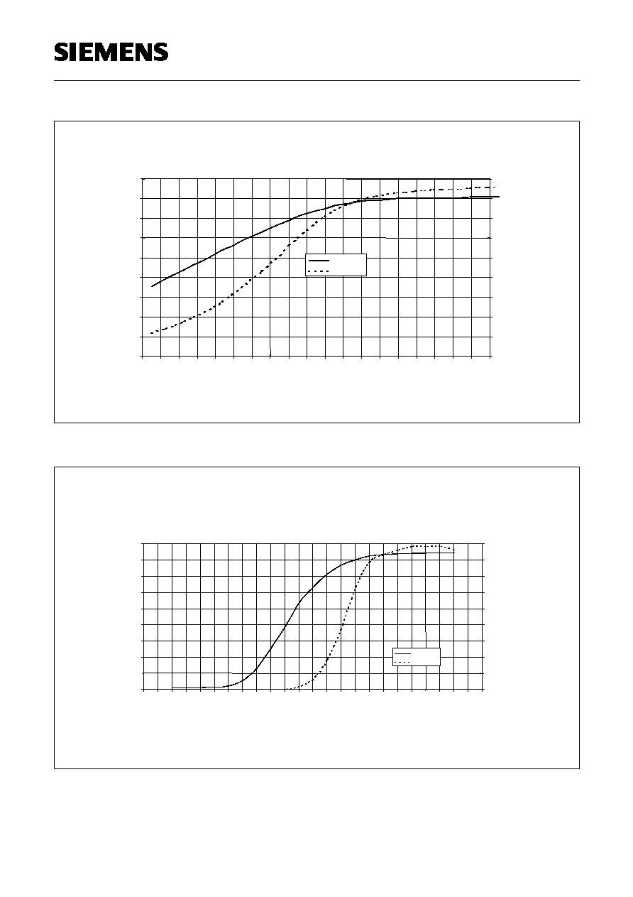
Pout and PAE vs. Pin
( V
D
=V
aux
=3.5V, V
Con
=2.2V, CLK=10MHz/3.5V/0V, f=1.75GHz, duty cycle 10%, t
on
=0.33ms )
18
20
22
24
26
28
30
32
34
36
-15
-14
-13
-12
-11
-10
-9
-8
-7
-6
-5
-4
-3
-2
-1
0
1
2
3
4
Pin [dBm]
Po
ut
[d
B
m]
0
5
10
15
20
25
30
35
40
45
P
A
E
[%
Pout [dBm]
PAE [%]
Pout and PAE vs. Vcon
( V
D
=Vaux=3.5V, CLK=10MHz/3.5V/0V,f=1.75GHz,P
in
=0dBm, duty cycle 10%, ton=0.33ms )
-50
-40
-30
-20
-10
0
10
20
30
40
0
0,1
0,2
0,3
0,4
0,5
0,6
0,7
0,8
0,9
1
1,1
1,2
1,3
1,4
1,5
1,6
1,7
1,8
1,9
2
2,1
2,2
2,3
2,4
Vcon [V]
Po
ut
[d
B
m]
0
5
10
15
20
25
30
35
40
45
PA
E
[%]
Pout [dBm]
PAE [%]
Semiconductor Group
7
1998-11-01

CGY 184
Siemens Aktiengesellschaft
8
23.07.97
HL HF PE GaAs
Output power at different temperatures
( V
D
=V
AUX
=3.5V, V
Con
=2.2V, CLK=0V/3.5V/10MHz, f=1.75GHz, P
in
=0dBm, duty cycle 10%, t
on
=0.33ms )
20
21
22
23
24
25
26
27
28
29
30
31
32
33
34
35
36
-15
-14
-13
-12
-11
-10
-9
-8
-7
-6
-5
-4
-3
-2
-1
0
1
2
3
4
5
Pin [dBm]
T=-20∞C
T=25∞C
T=85∞C
Power added efficiency at different temperatures
( V
D
=V
AUX
=3.5V, V
Con
=2.2V, CLK=0V/3.5V/10MHz, f=1.75GHz, P
in
=0dBm, duty cycle 10%, t
on
=0.33ms )
0
5
10
15
20
25
30
35
40
45
-15
-14
-13
-12
-11
-10
-9
-8
-7
-6
-5
-4
-3
-2
-1
0
1
2
3
4
5
Pin [dBm]
T=-20∞C
T=25∞C
T=85∞C
Semiconductor Group
8
1998-11-01

CGY 184
Siemens Aktiengesellschaft
9
23.07.97
HL HF PE GaAs
AM ≠ PM Conversion:
( Conditions: V
D
=V
AUX
=3.5V, f=1.75GHz, CLK=10MHz/3.5V/0V, P
out
controlled by V
Con
)
V
Con
[V]
[deg/dB]
P
out
[dBm]
2,2
2,8
34,53
2,1
3
34,53
2
2,7
34,37
1,9
2,6
34,2
1,8
2,5
33,87
1,7
2,4
33,37
1,6
1,5
32,37
1,5
0,5
30,2
1,4
-0,3
26,7
1,3
-0,2
21,2
1,2
-0,2
12,87
1,1
0,4
3,37
1
-0,2
-11,63
0,9
0,3
-24,8
CGY184
P
out
vs. V
C
( V
D
=V
AUX
=3.5V, CLK=3.5V/0V/13MHz, f=1.75GHz, duty cycle 10%, t
on
=0.33ms )
-50
-40
-30
-20
-10
0
10
20
30
40
0
0,2
0,4
0,6
0,8
1
1,2
1,4
1,6
1,8
2
2,2
V
Con
[V]
T=25∞C
T=-20∞C
T=85∞C
Semiconductor Group
9
1998-11-01
CGY 184
Siemens Aktiengesellschaft
10
23.07.97
HL HF PE GaAs
AM - PM - conversion
vs. Pout
(V
D
=V
AUX
=3.5V, CLK=10MHz/3.5V/0V,P
in
=0dBm, f=1.75GHz, duty cycle 10%, T=25∞C)
-0,5
0
0,5
1
1,5
2
2,5
3
3,5
-25
-20
-15
-10
-5
0
5
10
15
20
25
30
35
Pout [dBm]
[d
eg
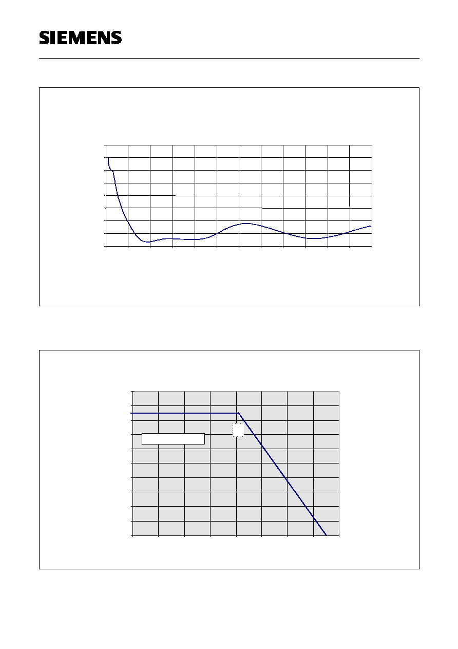
Ptotmax in mW
82
0
1000
2000
3000
4000
5000
6000
7000
8000
9000
10000
0
20
40
60
80
100
120
140
160
Tem perature Tc in ∞C
P
o
w
e
r D
i
s
s
i
p
a
tio
n
in
m
W
Ptot max = f ( Tc )
Pt t
Semiconductor Group
10
1998-11-01

CGY 184
Siemens Aktiengesellschaft
11
23.07.97
HL HF PE GaAs
Thermal Resistance and Temperature Considerations:
Because the MW16 heat sink is not easily accessible to a temperature measurment the
thermal resistance is defined as R
thJC
using the case temperature T
C
l
Calculation of Junction Temperature T
J
:
T
J
= T
C
+ R
thJC
* P
tot
l
Measurment of Case Temperature T
C
:
Tc should be measured in operation at the upper side of the case where the temperature
is highest. Small thermoelements
1mm (thin wires, thermopaste) and thermopapers
with low heat dissipation are well suited.
P C B
Junction ( J )
Case ( C )
Thermoelement for Tcase
Ambient ( A )
soldered Heatsink
Semiconductor Group
11
1998-11-01

CGY 184
Siemens Aktiengesellschaft
12
23.07.97
HL HF PE GaAs
CGY184 application board:
Layout size is 32mm x 19mm
Connections:
l
Vd
2.7 to 6VDC, pulsed (PCN: 12,5% duty cycle, ton=0.577ms)
l
Vaux
2.7 to 6VDC
l
Vcontrol 0.2 to 2.2VDC (0.2V: min Pout, 2.2V: max Pout)
l
CLK
5 MHz to 15 MHz (with a 10uH inductor)
or 150 kHz to 250 kHz (with a 100uH inductor instaed of the 10uH)
(rectangular signal, 50% duty, 0 Volt to Vd voltage level)
Power on sequence:
1.
continuous clock (CLK) on
2.
turn on Vaux ==> check negative voltage at pin#16 (-4......-10V)
3.
turn on Vcon (may be at the same time as 2)
turn on Drainvoltage Vd
turn on Input Power
Operation without using the negative voltage generator:
If you don't want to use the internal negative voltage generator, you can also apply -4....-6 V
at pin#15 (Vneg-Pin). In this case the passive devices at the pins 1, 14 and 16 are not
necessary (1 inductor and 3 capacitors).
3k 9
1 n
10
u
H
BC
8
4
8
B
47
n
68
0R
1 n
1 n
B AS
4 0-0
4 W
4,7
µ
1n
33
0
p
1n
5p
2.2nH
33
n
H
33p
1p
33p
15p
120 p
Semiconductor Group
12
1998-11-01

CGY 184
Siemens Aktiengesellschaft
13
23.07.97
HL HF PE GaAs
Part List:
CGY184
Negative Voltage Generator
L1
L2
C1
C2
C3
C4
C5
C6
C7
C8
C9
C10
33nH*
2.2nH**
4.7
µ
F
120pF
5pF
1pF
33pF
1nF
330pF
15pF
1nF
33pF
D1
T1
L11
C11
C12
C13
C14
R11
R12
BAS40-04W
BC848B
10uH***
1nF
1nF
47nF
1nF
3.8kOhm
680Ohm
*
33nH SMD-Inductor for drain3: Part Number BV1250 distribution by
Horst David GmbH, 85375 Neufarn, Germany
Phone-No ..8165/9548-0 , Fax-No ..8165/9548-28
**
Toko Type LL1608-FH Chip Induktor
*** Chip-Induktor Simid02
(Siemens-Matsushita Ordering-Code: B82422-A1103-K100 )
CGY184
Vcon
RF IN
Vd
RF OUT
C5
C3
(Vneg)
Vaux
C11
C13
R11
C14
C12
L11
R12
T1
D1.1
D1.2
CLK
C2
C1
L1
L2
VD1
VD2
RFout
Vcon
Vneg
GND1
GND2
RFin
RFout
RFout
C4
VD3
C6
C7
C8
C9
C10
Semiconductor Group
13
1998-11-01

CGY 184
Siemens Aktiengesellschaft
14
23.07.97
HL HF PE GaAs
Semiconductor Device Outline MW16
Published by Siemens AG, Bereich Bauelemente, Vertrieb, Produkt-Information,
Balanstraþe 73, D-81541 M¸nchen
copyright Siemens AG 1996. All Rights Reserved
As far as patents or other rights of third parties are concerned, liability is only assumed for
components per se, not for applications, processes and circuits implemented within
components or assemblies.
The information describes the type of component and shall not be considered as assured
characteristics.
Terms of delivery and rights to change design reserved.
For questions on technology, delivery and prices please contact the Offices of
Semiconductor Group in Germany or the Siemens Companies and Representatives world-
wide (see address list).
Due to technical requirements components may contain dangerous substances. For
information on the type in question please contact your nearest Siemens Office,
Semiconductor Group.
Siemens AG is an approved CECC manufacturer
Semiconductor Group
14
1998-11-01