
CGY 121 A
Siemens Aktiengesellschaft
1
23.06.98
HL HF PE GaAs1
GaAs MMIC
Preliminary Datasheet
l
Variable gain amplifier
(MMIC-Amplifier) for mobile communication
l
Typical Gain Control range over 50dB
l
Positive Control Voltage
l
50
input and output matched
l
Low power consumption
l
Operating voltage range: 2.7 to 6 V
l
Frequency range 800 MHz ... 2.5 GHz
ESD: Electrostatic discharge sensitive device,
observe handling precautions!
Type
Marking
Ordering code
(taped)
Package
1)
CGY 121 A
Y9S
Q-62702-G66
MW-6
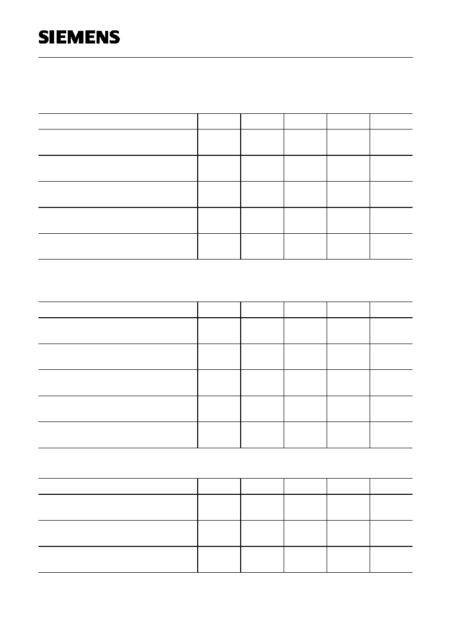
Maximum ratings
Characteristics
Symbol
max. Value
Unit
Drain voltage
VD
8
V
Neg. supply voltage
VG
-8
V
Pos. control voltage
Vcon
4
V
Channel temperature
TCh
150
∞C
Storage temperature range
Tstg
-55...+150
∞C
Total power dissipation (TS < 81∞C) 2)
Ptot
550
mW
Thermal resistance
Characteristics
Symbol
max. Value
Unit
Channel-soldering point (GND)
RthChS
125
K/W
1)
Dimensions see page 9.
2)
Please care for sufficient heat dissipation on the pcb!
*)
Pin-out changed compared to CGY120: 180∞ rotation
6
5
4
3
2
1
Vd1
RF-GND
RF-in; -Vg
RF-GND
Vd2; RF-out
Vcontrol
Semiconductor Group
1
1998-11-01
Semiconductor Group
1
1998-11-01

CGY 121 A
Siemens Aktiengesellschaft
2
23.06.98
HL HF PE GaAs1
Functional block diagram:
Pin #
Name
Configuration
1
VD2 /
Pout
Drain voltage 2nd stage / RF-0utput
2
RF-Gnd
3
VD1
Drain voltage 1st stage
4
VG / Pin
Negative voltage at current control circuit (-4V) / RF-Input
5
RF-Gnd
6
Vcontrol
Positive voltage for gain control (0V....3V)
Pin / -VG(4)
Pout (1)
Vcon (6)
GND (2, 5)
VD1 (3)
VD2 (1)
Control
Circuit
Semiconductor Group
2
1998-11-01
Semiconductor Group
2
1998-11-01
CGY 121 A
Siemens Aktiengesellschaft
3
23.06.98
HL HF PE GaAs1
Electrical characteristics
(
TA = 25∞C, f = 900 MHz, Vg = -4V, RS = RL = 50
unless otherwise specified)
Characteristics
Symbol
min
typ
max
Unit
Power Gain
Vd=3V; I=45mA; Vcon=3V
G
17
19
-
dB
Input return loss
Vd=3V; I=45mA; Vcon=3V
RLin
-
11
-
dB
Output return loss
Vd=3V; I=45mA; Vcon=3V
RLout
-
10
-
dB
Gain Control Range
Vcon=3 V ... 0V; Vd=3V; I=45mA
dG
48
53
-
dB
1dB gain compression
Vd=3V; I=45mA; Vcon=3V
P1dB
-
14
-
dBm
Electrical characteristics
(
TA = 25∞C ,f = 1800 MHz, Vg=-4V, RS = RL = 50
unless otherwise specified)
Characteristics
Symbol
min
typ
max
Unit
Power Gain
Vd=3V; I=45mA; Vcon=3V
G
15.5
17.5
-
dB
Input return loss
Vd=3V; I=45mA; Vcon=3V
RLin
-
10
-
dB
Output return loss
Vd=3V; I=45mA; Vcon=3V
RLout
-
8.5
-
dB
Gain Control Range
Vcon=3 V ... 0V; Vd=3V; I=45mA
dG
48
53
-
dB
1dB gain compression
Vd=3V; I=45mA; Vcon=3V
P1dB
-
14
-
dBm
DC characteristics
Characteristics
Symbol
min
typ
max
Unit
Gate current (Pin 4)
Vg=-4V
Ig
-
1.0
-
mA
Control current (Pin 6)
Vg=-4V; Vcon=0V...3V
Ic
-
0.5
-
mA
Supply current
Vg = -4V; Vcon = 3V
Id
-
45
-
mA
Semiconductor Group
3
1998-11-01
Semiconductor Group
3
1998-11-01

CGY 121 A
Siemens Aktiengesellschaft
4
23.06.98
HL HF PE GaAs1
Application Circuit
f = 900 MHz
CGY121
Input
50 Ohm
Output
50 Ohm
Vg
GND
Vcontrol
Vd
C4
R3
C1
C2
2,5
4
1
6
3
L2
C5
R1
R2
C3
L1
C
G
Y
1
2
1
C1
C2
C3
C4
C5
R1
R2
R3
L1
L2
Semiconductor Group
4
1998-11-01
Semiconductor Group
4
1998-11-01

CGY 121 A
Siemens Aktiengesellschaft
5
23.06.98
HL HF PE GaAs1
Parts List
Frequency
900 MHz
C1, C2 (Siemens Size 0603)
22 pF
0603
C3, C4 (Siemens Size 0603)
100 nF
0603
C5 (Siemens Size 0603)
47 nF
0603
L1 (Coilcraft 0805CS-150XKBC)
15 nH
0805
L2 (Coilcraft 0805CS-270XMBC)
27 nH
0805
R1 (Siemens B 54102-A1271-J60)
270 Ohm
0805
R2 (Siemens B 54102-A1120-J60)
12 Ohm
0805
R3
6.8 Ohm
0805
Application Circuit
f = 1900 MHz
CGY121
Input
50 Ohm
Output
50 Ohm
Vg
GND
Vcontrol
Vd
C4
R3
C1
C2
2,5
4
1
6
3
C5
R1
R2
C3
L1
C6
Semiconductor Group
5
1998-11-01
Semiconductor Group
5
1998-11-01

CGY 121 A
Siemens Aktiengesellschaft
6
23.06.98
HL HF PE GaAs1
Parts List
Frequency
1900 MHz
C1, C2 (Siemens size 0603)
12 pF
0603
C3, C4 (Siemens size 0603)
100 nF
0603
C5 (Siemens size 0603)
47 nF
0603
C6 (Siemens size 0603)
1.2 pF
0603
L1 (Coilcraft 0805CS-150XKBC)
15 nH
0805
R1 (Siemens B 54102-A1271-J60)
270 Ohm
0805
R2 (Siemens B 54102-A1120-J60)
12 Ohm
0805
R3
2.7 Ohm
0805
Semiconductor Group
6
1998-11-01
Semiconductor Group
6
1998-11-01

CGY 121 A
Siemens Aktiengesellschaft
7
23.06.98
HL HF PE GaAs1
Gain vs. Vcontrol
Operating Conditions : Vd=3V, Vg=-4V, f = 1.9GHz, Pin=-10dBm
Total Power Dissipation Ptot = f(Ts)
-40
-30
-20
-10
0
10
20
30
0
0,5
1
1,5
2
2,5
3
3,5
Vcontrol [V]
G
a
in [
d
B
]
Gain [dB] -20∞ C
Gain [dB] +25∞ C
Gain [dB] +70∞ C
Ptotmax in mW
81∞C
0
100
200
300
400
500
600
700
0
10
20
30
40
50
60
70
80
90
100
110
120
130
140
150
Soldering Point Temperature Ts in ∞C
P
o
wer
Dissip
a
tio
n
in
m
W
P
totmax
Semiconductor Group
7
1998-11-01
Semiconductor Group
7
1998-11-01

CGY 121 A
Siemens Aktiengesellschaft
8
23.06.98
HL HF PE GaAs1
Semiconductor Device Outline MW-6
Published by Siemens AG, Bereich Halbleiter, Marketing-Kommunikation,
Balanstraþe 73, D-81541 M¸nchen.
copyright Siemens AG 1997. All Rights Reserved.
As far as patents or other rights of third parties are concerned, liability is only assumed for
components per se, not for applications, processes and cirucits implemented within
components or assemblies.
The information describes the type of component and shall not be considered as assured
characteristics.
Terms of delivery and rights to change design reserved.
For questions on technology, delivery, and prices please contact the Offices of
Semiconductor Group in Germany or the Siemens Companies and Representatives
worldwide (see address list).
Due to technical requirements components may contain dangerous substances. For
information on the type in question please contact your nearest Siemens Office,
Semiconductor Group.
Siemens AG is an approved CECC manufacturer.
Semiconductor Group
8
1998-11-01
Semiconductor Group
8
1998-11-01