 | –≠–ª–µ–∫—Ç—Ä–æ–Ω–Ω—ã–π –∫–æ–º–ø–æ–Ω–µ–Ω—Ç: Q62702G74 | –°–∫–∞—á–∞—Ç—å:  PDF PDF  ZIP ZIP |
CGY 191
Siemens Aktiengesellschaft
1
23.07.1998
HL HF PE GaAs 1/Fo
GaAs MMIC
l
Dual mode power amplifier for CDMA /TDMA
portable cellular phones
l
29 dBm linear output power@ PAE=40% typ.
l
Fully integrated 2 stage amplifier
l
Power ramp control
l
Input matched to 50 ohms, simple output match
ESD: Electrostatic discharge sensitive device,
observe handling precautions!
Type
Marking
Ordering code
(taped)
Package
CGY 191
CGY 191
Q62702G74
MW 16
Maximum ratings
Characteristics
Symbol
max. Value
Unit
Positive supply voltage
VD
9
V
Supply current
ID
4
A
Channel temperature
TCh
150
∞C
Storage temperature
Tstg
-55...+150
∞C
Pulse peak power dissipation
PPulse
tbd
W
Total power dissipation
(Ts
80 ∞C)
Ts: Temperature at soldering point
Ptot
tbd
W
Thermal Resistance
Characteristics
Symbol
max. Value
Unit
Channel-soldering point
RthChS
11
K/W
Semiconductor Group
1
1998-11-01
CGY 191
Siemens Aktiengesellschaft
2
23.07.1998
HL HF PE GaAs 1/Fo
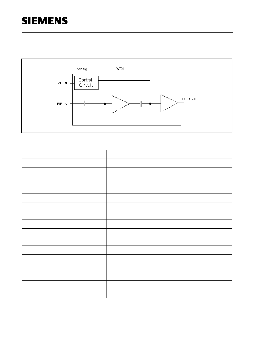
Functional Block Diagram:
Pin Configuration:
Pin #
Configuration
1
n. c.
2
n. c.
3
Vcon
Control voltage
4
Vneg
Negative voltage
5
n. c.
6
RF IN
RF IN PCS Band
7
n. c.
8
VD 1
Drain voltage preamplifier stage
9
n. c.
10
n. c.
11
RF out
RF out / drain voltage final stage
12
RF out
RF out / drain voltage final stage
13
RF out
RF out / drain voltage final stage
14
RF out
RF out / drain voltage final stage
15
n. c.
16
n. c.
Semiconductor Group
2
1998-11-01

CGY 191
Siemens Aktiengesellschaft
3
23.07.1998
HL HF PE GaAs 1/Fo
Electrical Characteristics
(TA = 25∞C , ZS=ZL=50 Ohm, VD=3.5V, IDq=300mA, unless otherwise specified )
Characteristics
Symbol
min
typ
max
Unit
Frequency range
f
1850
1910
MHz
Duty cycle
t
ON
/t
OFF
100
%
TDMA output power
P
29
dBm
TDMA gain at max. output
G
24
dB
CDMA output power
P
29
dBm
CDMA gain at max. output
G
24
dB
Power ramping characteristic
Full output power
Pinch off
V
contr
2.5
0.5
V
Adjacent Channel Power CDMA
1.25 MHz offset (PCS band)
1.98 MHz offset
P
adj
/P
main
-45
-54
dBc @
30kHz
Adjacent channel power TDMA
adjacent
alternate
2nd alternate
P
adj
/P
main
-28
-45
-45
dBc @
30kHz
TDMA DC to RF efficiency
@Padj=-26dBc
at max. output
PAE
40
%
CDMA DC to RF efficiency
@Padj=-42dBc
at max. output
at 10 dBm output power
PAE
40
4
%
Receive band noise power density
( 1930 to 1990 MHz )
P
RX
-145
dBm/Hz
DC supply voltage range
VD
2.9
3.5
4.0
V
Negative supply voltage range
Vneg
-5.0
-7.0
V
Standby current @Vcon=0V
I
pwr dwn
500
µ
A
Semiconductor Group
3
1998-11-01

CGY 191
Siemens Aktiengesellschaft
4
23.07.1998
HL HF PE GaAs 1/Fo
Characteristics
Symbol
min
typ
max
Unit
Quiescent current
300
mA
Current consumption at V
Contr
I
Control
2
mA
Current consumption at V
NEG
I
NEG
2
mA
Operating temperature range
-30
+85
∞C
Power on sequence:
1. connect negative voltage to PA
2. connect control voltage to PA
3. turn on Vd
4. turn on Pin
To switch off the device please use reverse sequence.
Application Circuit:
100p
C9
C15
33n
IC1
CGY191
10
NC10
9
NC9
2
NC2
11
VD2/RFout1
17
GND (backside MW16)
4
Vneg
7
NC7
8
VD1
15
NC15
16
NC16
3
Vcon
6
RFin
12
VD2/RFout2
13
VD2/RFout3
14
VD2/RFout4
5
NC5
1
NC1
R
1
3
k
9
C
8
3
p
9
H
Q
1
u
0
C
6
C
5
1
u
0
1
u
0
C
4
C
3
1
u
0
L
2
3
3
n
H
L
1
1
0
u
H
RFout
CLK
RFin
BC848B
V2
BAS 40-04
V1
3
2
1
Vaux
Vcon
Vd
R
2
6
8
0
R
C14
1n0
3
3
n
C
1
2
C13
1n0
10n
C1
C
1
1
1
0
n
C
7
1
0
0
p
C10
100p
L
3
3
3
n
H
Semiconductor Group
4
1998-11-01

CGY 191
Siemens Aktiengesellschaft
5
23.07.1998
HL HF PE GaAs 1/Fo
Evaluation Board:
Evaluation Board Parts List:
Part Type
Position
Description
Manufacturer
Part Number
Capacitor
C1, C11
10nF 0402
Siemens
Capacitor
C7, C9, C10
100pF 0402
Siemens
Capacitor
C8
3,9pF 0603 High
Q
AVX
06035J3R9BBT
Capacitor
C3, C4, C5, C6
1uF 1206
Siemens
Capacitor
C12, C15
33nF 0402
Siemens
Capacitor
C13, C14
1nF 0402
Siemens
Inductor
L1
10uH
Siemens
Air Coil
L2
33nH
Horst David
GmbH
PN/BV 1250
Inductor
L3
33nH 0603
Toko
Resistor
R1
3,9k
Siemens
Resistor
R2
680 Ohm
Siemens
Diode
V1
BAS40-04W
Siemens
Transistor
V2
BC848B
Siemens
Substrate
FR4, h=0.2mm,
r
=4.5
Siemens
RFout
C
G
Y
1
9
1
S
I
E
M
E
N
S
PA
PCS Band
CLK
Vcon
Vaux
Vd
RFin
L2
R
F
o
u
t
CLK
R
F
i
n
Vaux
Vcon
Vd
C4
C3
C
7
C
5
C
6
L
3
C9
C
8
IC1
C10
C
1
C
1
1
C
1
5
V
1
C12
C
1
4
L
1
R
2
R
1
C
1
3
V
2
Semiconductor Group
5
1998-11-01

CGY 191
Siemens Aktiengesellschaft
6
23.07.1998
HL HF PE GaAs 1/Fo
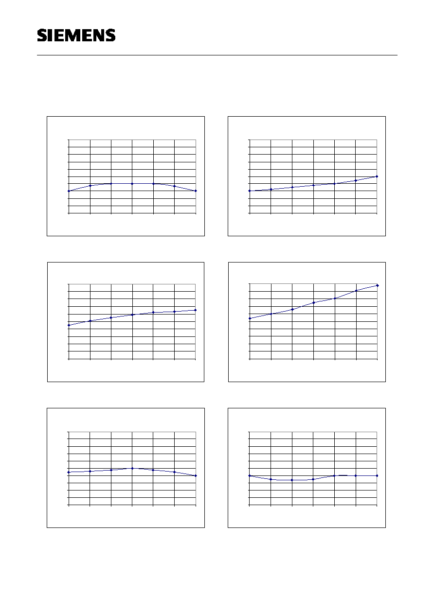
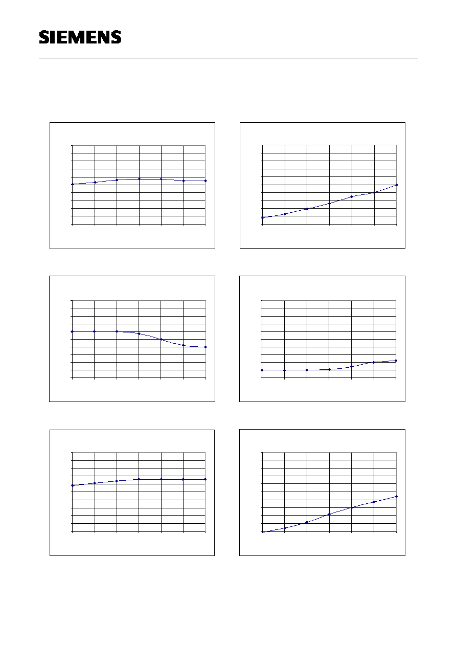
Typical Performance in CDMA Operation Mode:
CDMA Mode: Pout, PAE & Id vs. Pin
Vd=3,5V, Iq=250m A, f=1880 MHz, T=25∞C
0
5
10
15
20
25
30
35
40
-10
-8
-6
-4
-2
0
2
4
6
8
Pin [dBm]
P
o
ut
[dB
m
], P
A
E
[%
]
0
100
200
300
400
500
600
700
800
Id [m
A
]
Pout [dBm]
PAE [%]
Id [mA]
CDMA Mode: ACPR & TG vs. Pout
Vd=3,5V, Iq=250m A, f=1880 MHz, T=25∞C
0
10
20
30
40
50
60
70
80
14
16
18
20
22
24
26
28
30
Pout [dBm]
ACPR [
d
B
c
]
18
19
20
21
22
23
24
25
26
T
G
[d
B
]
ACP1,25 [dBc]
ACP1,98 [dBc]
TG [dB]
CDMA Mode : ACPR @1,25MHz Offset vs. f
Vd=3,0V, Pout=28dBm , Iq=250m A
40
41
42
43
44
45
46
47
48
49
50
1850
1860
1870
1880
1890
1900
1910
f [MHz]
AC
PR
[
d
Bc
]
CDMA Mode: ACPR @1,98MHz Offse t vs . f
Vd=3,0V, Pout=28dBm , Iq=250m A
50
51
52
53
54
55
56
57
58
59
60
1850
1860
1870
1880
1890
1900
1910
f [MHz]
AC
PR
[
d
Bc
]
CDMA Mode: Gain vs . f
Vd=3,0V, Pout=28dBm , Iq=250m A
15
16
17
18
19
20
21
22
23
24
25
1850
1860
1870
1880
1890
1900
1910
f [MHz]
T
G
[d
B
]
CDMA Mode : PAE vs. f
Vd=3,0V, Pout=28dBm , Iq=250m A
30
32
34
36
38
40
42
1850
1860
1870
1880
1890
1900
1910
f [MHz]
PA
E [
%
]
Semiconductor Group
6
1998-11-01
CGY 191
Siemens Aktiengesellschaft
7
23.07.1998
HL HF PE GaAs 1/Fo
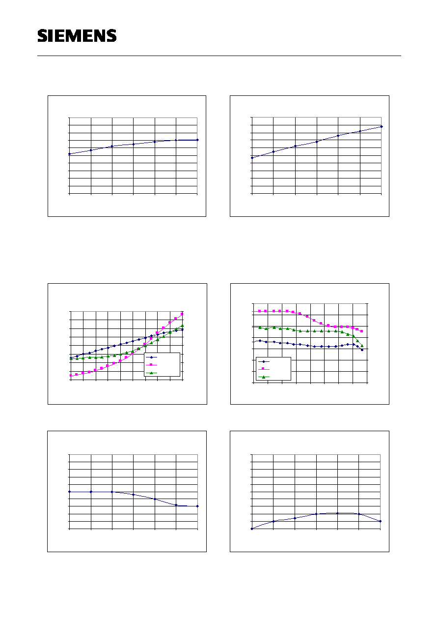
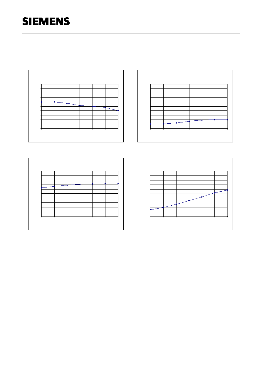
CDMA Mode: ACPR @1,25MHz Offs et vs. f
Vd=3,5V, Pout=29dBm , Iq=250m A
40
41
42
43
44
45
46
47
48
49
50
1850
1860
1870
1880
1890
1900
1910
f [MHz]
AC
PR
[
d
Bc
]
CDMA Mode: ACPR @1,98MHz Offset vs. f
Vd=3,5V, Pout=29dBm , Iq=250m A
50
51
52
53
54
55
56
57
58
59
60
1850
1860
1870
1880
1890
1900
1910
f [MHz]
AC
PR
[
d
Bc
]
CDMA Mode: Gain vs. f
Vd=3,5V, Pout=29dBm , Iq=250m A
15
16
17
18
19
20
21
22
23
24
25
1850
1860
1870
1880
1890
1900
1910
f [MHz]
TG
[
d
B
]
CDMA Mode: PAE vs. f
Vd=3,5V, Pout=29dBm , Iq=250m A
30
31
32
33
34
35
36
37
38
39
40
1850
1860
1870
1880
1890
1900
1910
f [MHz]
PAE [
%
]
CDMA Mode: ACPR @1,25MHz Offset vs. f
Vd=4V, Pout=30dBm , Iq=250m A
40
41
42
43
44
45
46
47
48
49
50
1850
1860
1870
1880
1890
1900
1910
f [MHz]
AC
PR
[
d
Bc
]
CDMA Mode : ACPR @1,98MHz Offset vs. f
Vd=4V, Pout=30dBm , Iq=250m A
50
51
52
53
54
55
56
57
58
59
60
1850
1860
1870
1880
1890
1900
1910
f [MHz]
AC
PR
[
d
Bc
]
Semiconductor Group
7
1998-11-01
CGY 191
Siemens Aktiengesellschaft
8
23.07.1998
HL HF PE GaAs 1/Fo
CDMA Mode: Gain vs. f
Vd=4V, Pout=30dBm , Iq=250m A
15
16
17
18
19
20
21
22
23
24
25
1850
1860
1870
1880
1890
1900
1910
f [MHz]
T
G
[d
B
]
CDMA Mode: PAE vs. f
Vd=4V, Pout=30dBm , Iq=250m A
30
31
32
33
34
35
36
37
38
39
40
1850
1860
1870
1880
1890
1900
1910
f [MHz]
PAE [
%
]
Typical Performance in TDMA Operation Mode:
TDMA Mode: Pout, PAE & Id vs. Pin
Vd=3,5V, Iq=250m A, f=1880 MHz, T=25∞C
0
5
10
15
20
25
30
35
40
-10
-8
-6
-4
-2
0
2
4
6
8
Pin [dBm]
Po
u
t
[
d
Bm
]
,
PA
E [
%
]
0
100
200
300
400
500
600
700
800
Id [
m
A
]
Pout [dBm]
PAE [%]
Id [mA]
TDMA Mode : ACPR & TG vs. Pout
Vd=3,5V, Iq=250m A, f=1880 MHz, T=25∞C
0
10
20
30
40
50
60
70
14
16
18
20
22
24
26
28
30
Pout [dBm]
ACPR [
d
B
c
]
18
19
20
21
22
23
24
25
T
G
[d
B
]
Padj [dBc]
Palt [dBc]
TG [dB]
TDMA Mode: Padj vs. f
Vd=3,0V, Pout=28dBm , Iq=250m A
25
26
27
28
29
30
31
32
33
34
35
1850
1860
1870
1880
1890
1900
1910
f [MHz]
AC
PR
[
d
Bc
]
TDMA Mode: Palt vs. f
Vd=3,0V, Pout=28dBm , Iq=250m A
45
46
47
48
49
50
51
52
53
54
55
1850
1860
1870
1880
1890
1900
1910
f [MHz]
AC
PR
[
d
Bc
]
Semiconductor Group
8
1998-11-01
CGY 191
Siemens Aktiengesellschaft
9
23.07.1998
HL HF PE GaAs 1/Fo
TDMA Mode: Gain vs. f
Vd=3V, Pout=28dBm, Iq=250mA
15
16
17
18
19
20
21
22
23
24
25
1850
1860
1870
1880
1890
1900
1910
f [MHz]
TG
[dB
]
TDMA Mode: PAE vs. f
Vd=3V, Pout=28dBm , Iq=250m A
35
36
37
38
39
40
41
42
43
44
45
1850
1860
1870
1880
1890
1900
1910
f [MHz]
PAE [
%
]
TDMA Mode: Padj vs. f
Vd=3,5V, Pout=29dBm , Iq=250m A
25
26
27
28
29
30
31
32
33
34
35
1850
1860
1870
1880
1890
1900
1910
f [MHz]
AC
PR
[
d
Bc
]
TDMA Mode: Palt vs. f
Vd=3,5V, Pout=29dBm , Iq=250m A
45
46
47
48
49
50
51
52
53
54
55
1850
1860
1870
1880
1890
1900
1910
f [MHz]
AC
PR
[
d
Bc
]
TDMA Mode: Gain vs. f
Vd=3,5V, Pout=29dBm , Iq=250m A
15
16
17
18
19
20
21
22
23
24
25
1850
1860
1870
1880
1890
1900
1910
f [MHz]
T
G
[d
B
]
TDMA Mode: PAE vs. f
Vd=3,5V, Pout=29dBm , Iq=250m A
35
36
37
38
39
40
41
42
43
44
45
1850
1860
1870
1880
1890
1900
1910
f [MHz]
PAE [
%
]
Semiconductor Group
9
1998-11-01
CGY 191
Siemens Aktiengesellschaft
10
23.07.1998
HL HF PE GaAs 1/Fo
TDMA Mode: Padj vs. f
Vd=4V, Pout=30dBm , Iq=250m A
25
26
27
28
29
30
31
32
33
34
35
1850
1860
1870
1880
1890
1900
1910
f [MHz]
AC
P
R
[
d
B
c
]
TDMA Mode: Palt vs. f
Vd=4V, Pout=30dBm , Iq=250m A
45
46
47
48
49
50
51
52
53
54
55
1850
1860
1870
1880
1890
1900
1910
f [MHz]
A
C
PR
[
d
Bc
]
TDMA Mode: Gain vs. f
Vd=4V, Pout=30dBm , Iq=250m A
15
16
17
18
19
20
21
22
23
24
25
1850
1860
1870
1880
1890
1900
1910
f [MHz]
T
G
[d
B
]
TDMA Mode: PAE vs. f
Vd=4V, Pout=30dBm , Iq=250m A
33
34
35
36
37
38
39
40
41
42
43
1850
1860
1870
1880
1890
1900
1910
f [MHz]
PAE [
%
]
Semiconductor Group
10
1998-11-01

CGY 191
Siemens Aktiengesellschaft
11
23.07.1998
HL HF PE GaAs 1/Fo
Published by Siemens AG, Bereich Bauelemente, Vertrieb,
Produkt-Information, Balanstraþe 73, D-81541 M¸nchen
copyright
Siemens AG 1996. All Rights Reserved
As far as patents or other rights of third parties are concerned, liability is only assumed for
components per se, not for applications, processes and circuits implemented within
components or assemblies.
The information describes the type of component and shall not be considered as assured
characteristics.
Terms of delivery and rights to change design reserved.
For questions on technology, delivery and prices please contact the Offices of
Semiconductor Group in Germany or the Siemens Companies and Representatives world-
wide (see address list).
Due to technical requirements components may contain dangerous substances. For
information on the type in question please contact your nearest Siemens Office,
Semiconductor Group.
Siemens AG is an approved CECC manufacturer.
Semiconductor Group
11
1998-11-01