Semiconductor Group
1
PNP Silicon Transistors
SMBT 5086
SMBT 5087
5.91
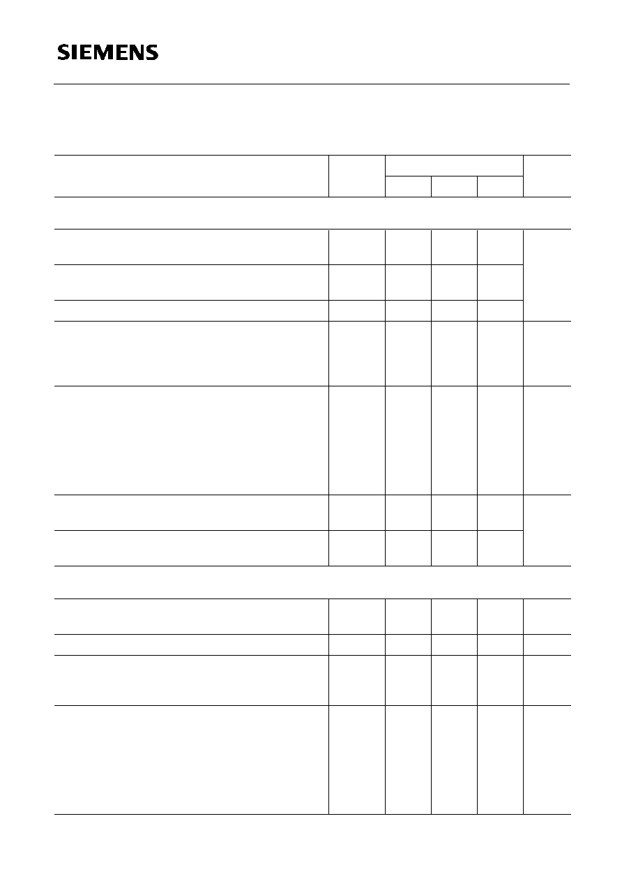
Maximum Ratings
Type
Ordering Code
(tape and reel)
Marking
Package
1)
Pin Configuration
SMBT 5086
SMBT 5087
Q62702-M0002
Q68000-A8319
s2P
s2Q
SOT-23
B
E
C
1
2
3
1)
For detailed information see chapter Package Outlines.
2)
Package mounted on epoxy pcb 40 mm
◊
40 mm
◊
1.5 mm/6 cm
2
Cu.
Parameter
Symbol
Values
Unit
Emitter-base voltage
V
EB0
Collector-base voltage
V
CB0
Junction temperature
T
j
∞C
Total power dissipation,
T
S
= 71 ∞C
P
tot
mW
Storage temperature range
T
stg
Collector-emitter voltage
V
CE0
V
Thermal Resistance
Junction - ambient
2)
R
th JA
310
K/W
3
330
150
≠ 65 ... + 150
50
Collector current
I
C
mA
50
Junction - soldering point
R
th JS
240
50
q
For AF input stages and driver applications
q
High current gain
q
Low collector-emitter saturation voltage
q
Low noise between 30 Hz and 15 kHz
Semiconductor Group
2
SMBT 5086
SMBT 5087
Electrical Characteristics
at
T
A
= 25 ∞C, unless otherwise specified.
V
Collector-emitter breakdown voltage
I
C
= 1 mA
V
(BR)CE0
50
≠
≠
nA
nA
µ
A
Collector-base cutoff current
V
CB
= 10 V,
I
E
= 0
V
CB
= 35 V,
I
E
= 0
V
CB
= 35 V,
I
E
= 0,
T
A
= 150 ∞C
I
CB0
≠
≠
≠
≠
≠
≠
10
50
20
Unit
Values
Parameter
Symbol
min.
typ.
max.
DC characteristics
Emitter-base breakdown voltage,
I
E
= 10
µ
A
V
(BR)EB0
3
≠
≠
V
Collector-emitter saturation voltage
1)
I
C
= 10 mA,
I
B
= 1 mA
V
CEsat
≠
≠
0.3
≠
DC current gain
I
C
= 100
µ
A,
V
CE
= 5 V
SMBT 5086
SMBT 5087
I
C
= 1 mA,
V
CE
= 5 V
SMBT 5086
SMBT 5087
I
C
= 10 mA,
V
CE
= 5 V
SMBT 5086
SMBT 5087
h
FE
150
250
150
250
150
250
≠
≠
≠
≠
≠
≠
500
800
≠
≠
≠
≠
MHz
Transition frequency
I
C
= 0.5 mA,
V
CE
= 5 V,
f
= 100 MHz
f
T
40
≠
≠
AC characteristics
≠
Small-signal current gain
I
C
= 1 mA,
V
CE
= 5 V,
f
= 1 kHz
SMBT 5086
I
C
= 1 mA,
V
CE
= 5 V,
f
= 1 kHz
SMBT 5087
h
fe
150
250
≠
≠
600
900
Collector-base breakdown voltage
I
C
= 100
µ
A
V
(BR)CB0
50
≠
≠
Base-emitter saturation voltage
1)
I
C
= 10 mA,
I
B
= 1 mA
V
BEsat
≠
≠
0.85
pF
Output capacitance,
V
CB
= 5 V,
f
= 1 MHz
C
obo
≠
≠
4
dB
dB
dB
dB
Noise figure
I
C
= 100
µ
A,
V
CE
= 5 V,
f
= 1 kHz,
R
S
= 3 k
SMBT 5086
SMBT 5087
I
C
= 2 mA,
V
CE
= 5 V,
f
= 10 Hz to 15 kHz,
R
S
= 10 k
SMBT 5086
SMBT 5087
NF
≠
≠
≠
≠
≠
≠
≠
≠
3
2
3
2
1)
Pulse test conditions:
t
300
µ
s,
D
2 %.