NPN-Silizium-Fototransistor
Silicon NPN Phototransistor
SFH 3400
Semiconductor Group
1
1998-04-27
Ma
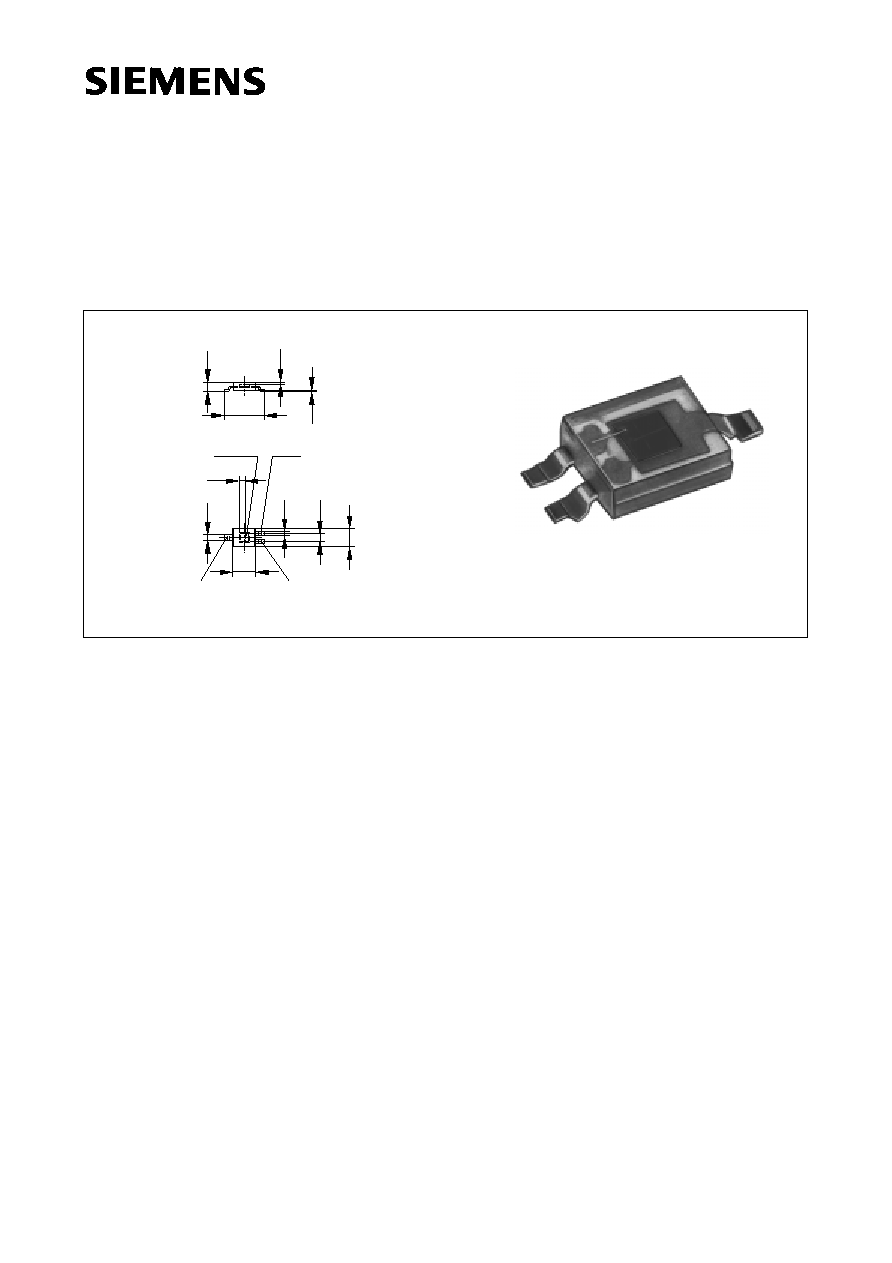
e in mm, wenn nicht anders angegeben/Dimensions in mm, unless otherwise specified.
GEO06953
0.5
0.3
1.9
2.1
0.6
0.8
2.5
2.7
0.3
connected
Emitter
Collector
4.8
4.4
1.1
1.0
0.2
0.3
0.0
0.1
Chip position
0.9
1.1
0.7
not
Active area
0.55
Wesentliche Merkmale
q
Speziell geeignet f�r Anwendungen im
Bereich von 460 nm bis 1080 nm
q
Hohe Linearit�t
q
SMT-Bauform ohne Basisanschlu�,
geeignet f�r Vapor Phase-L�ten und
IR-Reflow-L�ten (JEDEC level 4)
q
Nur gegurtet lieferbar
Anwendungen
q
Umgebungslicht-Detektor
q
Lichtschranken f�r Gleich- und Wechsel-
lichtbetrieb
q
Industrieelektronik
q
,,Messen/Steuern/Regeln"
Features
q
Especially suitable for applications from
460 nm to 1080 nm
q
High linearity
q
SMT package without base connection,
suitable for vapor phase and IR reflow
soldering (JEDEC level 4)
q
Available only on tape and reel
Applications
q
Ambient light detector
q
Photointerrupters
q
Industrial electronics
q
For control and drive circuits
SFH 3400
Semiconductor Group
2
1998-04-27
Grenzwerte
Maximum Ratings
Typ
Type
Bestellnummer
Ordering Code
Geh�use
Package
SFH 3400
Q62702-P1796
Klares Epoxy-Gie
harz, Kollektorkennzeichung:
breiter Anschlu�
Transparent epoxy resin, collector marking: broad
lead
SFH 3400-2
Q62702-P1103
SFH 3400-3
Q62702-P1805
Bezeichnung
Description
Symbol
Symbol
Wert
Value
Einheit
Unit
Betriebs- und Lagertemperatur
Operating and storage temperature range
T
op
;
T
stg
� 40 ... + 85
o
C
Kollektor-Emitterspannung
Collector-emitter voltage
V
CE
20
V
Kollektor-Emitterspannung,
t
< 120 s
Collector-emitter voltage
V
CE
70
V
Kollektorstrom
Collector current
I
C
50
mA
Kollektorspitzenstrom,
<
10
�
s
Collector surge current
I
CS
100
mA
Emitter-Kollektorspannung
Emitter-collector voltage
V
EC
7
V
Verlustleistung,
T
A
= 25
�
C
Total power dissipation
P
tot
120
mW
W�rmewiderstand f�r Montage auf PC-Board
Thermal resistance for mounting on pcb
R
thJA
450
K/W
SFH 3400
Semiconductor Group
3
1998-04-27
Kennwerte (
T
A
= 25
o
C,
= 950 nm)
Characteristics
Bezeichnung
Description
Symbol
Symbol
Wert
Value
Einheit
Unit
Wellenl�nge der max. Fotoempfindlichkeit
Wavelength of max. sensitivity
S max
850
nm
Spektraler Bereich der Fotoempfindlichkeit
S
= 10% von
S
max
Spectral range of sensitivity
S
= 10% of
S
max
460 ... 1080
nm
Bestrahlungsempfindliche Fl�che
Radiant sensitive area
A
0.55
mm
2
Abmessung der Chipfl�che
Dimensions of chip area
L
x
B
L
x
W
1 x 1
mm x mm
Abstand Chipoberfl�che zu Geh�useoberfl�che
Distance chip front to case surface
H
0.2 ... 0.3
mm
Halbwinkel
Half angle
�
60
Grad
deg.
Kapazit�t,
V
CE
= 0 V,
f
= 1 MHz,
E
= 0
Capacitance
C
CE
15
pF
Dunkelstrom
Dark current
V
CE
= 10 V,
E
= 0
I
CEO
10 (
200)
nA
SFH 3400
Semiconductor Group
4
1998-04-27
Die Fototransistoren werden nach ihrer Fotoempfindlichkeit gruppiert und mit arabischen
Ziffern gekennzeichnet.
The phototransistors are grouped according to their spectral sensitivity and distinguished
by arabian figures.
1)
I
PCEmin
ist der minimale Fotostrom der jeweiligen Gruppe
1)
I
PCEmin
is the min. photocurrent of the specified group
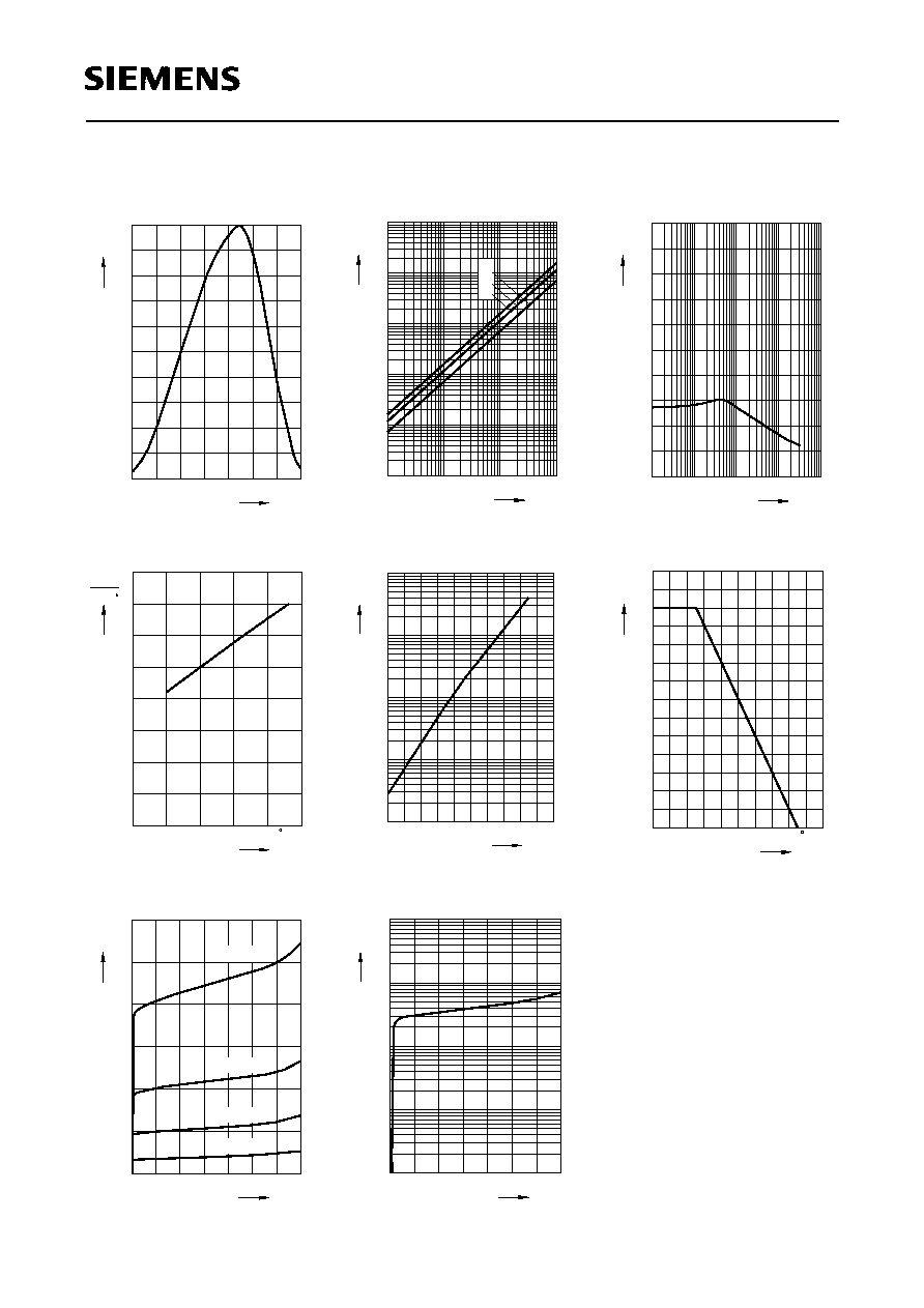
Directional characteristics
S
rel
=
f
(
)
Bezeichnung
Description
Symbol
Symbol
Wert
Value
Einheit
Unit
-1
-2
-3
Fotostrom,
=
950 nm
Photocurrent
E
e
= 0.1 mW/cm
2
,
V
CE
= 5 V
E
v
= 1000 Ix, Normlicht/standard
light A,
V
CE
= 5 V
I
PCE
I
PCE
63 ... 125
1.65
100 ... 200
2.6
160 ... 320
4.2
�
A
mA
Anstiegszeit/Abfallzeit
Rise and fall time
I
C
= 1 mA,
V
CC
= 5 V,
R
L
= 1 k
t
r
,
t
f
16
24
34
�
s
Kollektor-Emitter-
S�ttigungsspannung
Collector-emitter saturation voltage
I
C
=
I
PCEmin
1)
x 0.3,
E
e
= 0.1 mW/cm
2
V
CEsat
170
170
170
mV
OHF01402
90
80
70
60
50
40
30
20
10
20
40
60
80
100
120
0.4
0.6
0.8
1.0
0.2
0.4
0.6
0.8
1.0
100
0
0
0
Semiconductor Group
5
1998-04-27
SFH 3400
T
A
=
25
o
C,
=
950 nm
Rel.spectral sensitivity
S
rel
=
f
(
)
Photocurrent
I
PCE
=
f
(
T
A
),
V
CE
= 5 V, normalized to 25
�
C
Photocurrent
I
PCE
=
f
(
V
CE
)
Photocurrent
I
PCE
=
f
(
E
e
),
V
CE
= 5 V
Dark current
I
CEO
=
f
(
T
A
),
V
CE
= 10 V,
E
= 0
Dark current
I
CEO
=
f
(
V
CE
),
E
= 0
OHF02332
0
rel
S
400
10
20
30
40
50
60
70
80
%
100
500 600 700 800 900
nm 1100
T
OHF01524
A
0
-25
0.2
0.4
0.6
0.8
1.0
1.2
1.4
1.6
0
25
50
75
100
PCE
PCE
25
C
V
OHF00327
ce
0
0
10
20
30
40
50
60
70
V
mA
pce
1.0 mW/cm
0.5
1.0
1.5
2.0
2.5
3.0
2
2
0.5 mW/cm
0.25 mW/cm
2
0.1 mW/cm
2
E
OHF00326
e
-3
10
pce
-4
10
10
1
mA
2
mW/cm
10
-2
10
0
10
-3
10
-2
10
-1
0
10
1
2
3
T
OHF02342
A
0
CEO
-2
10
10
-1
10
0
10
1
10
2
nA
20
40
60
80
100
�C
V
OHF02341
CE
0
CEO
-2
10
10
-1
10
0
10
1
10
2
nA
10
20
30
40
50
70
V
Collector-emitter capacitance
C
CE
=
f
(
V
CE
),
f
= 1 MHz
Total power dissipation
P
tot
=
f
(
T
A
)
V
OHF02344
CE
CE
C
0
10
-2
-1
10
0
10
1
10
10
2
V
10
20
30
40
pF
50
T
OHF00309
A
0
tot
P
0
20
40
60
80 C 100
mW
20
40
60
80
100
120
140