Semiconductor Group
1
1998-08-27
Silizium-PIN-Fotodiode mit Tageslichtsperrfilter
Neu: in SMT und als Reverse Gullwing
Silicon PIN Photodiode with Daylight Filter
New: in SMT and as Reverse Gullwing
BPW 34 FA
BPW 34 FAS
BPW 34 FAS (E9087)
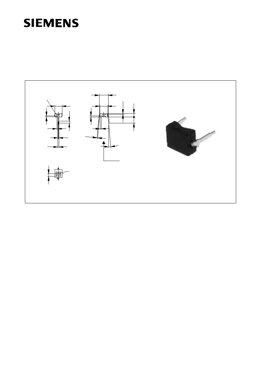
Maþe in mm, wenn nicht anders angegeben/Dimensions in mm, unless otherwise specified
GEO06643
4.0
3.7
4.3
4.5
5.4
4.9
0.6
0.4
0.6
0.4
1.2
0.7
0.3
0.5
0.8
0.6
Cathode marking
0.6
0.8
1.9
2.2
3.0
3.5
0.6
0.4
Chip position
0.4
0.6
0.35
0.2
0 ... 5∞
5.08 mm
spacing
Approx. weight 0.1 g
1.4
Photosensitive area
2.65 mm x 2.65 mm
1.8
feo06075
BPW 34 FA
Wesentliche Merkmale
q
Speziell geeignet f¸r den Wellenl‰ngen-
bereich von 830 nm bis 880 nm
q
Kurze Schaltzeit (typ. 20 ns)
q
DIL-Plastikbauform mit hoher
Packungsdichte
q
BPW 34 FAS/(E9087): geeignet f¸r
Vapor-Phase Lˆten und IR-Reflow Lˆten
Anwendungen
q
IR-Fernsteuerung von Fernseh- und
Rundfunkger‰ten, Videorecordern,
Ger‰tefernsteuerung
q
Lichtschranken f¸r Gleich- und
Wechsellichtbetrieb
Features
q
Especially suitable for the wavelength range
of 830 nm to 880 nm
q
Short switching time (typ. 20 ns)
q
DIL plastic package with high packing
density
q
BPW 34 FAS/(E9087): Suitable for
vapor-phase and IR-reflow soldering
Applications
q
IR-remote control of hi-fi and TV sets, video
tape recorders, remote controls of various
equipment
q
Photointerrupters

BPW 34 FA, BPW 34 FAS
BPW 34 FAS (E9087)
Semiconductor Group
2
1998-08-27
Maþe in mm, wenn nicht anders angegeben/Dimensions in mm, unless otherwise specified.
Typ
Type
Bestellnummer
Ordering Code
BPW 34 FA
Q62702-P1129
BPW 34 FAS
Q62702-P463
BPW 34 FAS (E9087)
Q62702-P1829
4.5
4.3
4.0
3.7
1.5
1.7
0.9
0.7
Photosensitive area
Cathode lead
GEO06863
0.3
6.7
6.2
1.2
1.1
0...0.1
Chip position
0...5∞
0.2
0.1
1.1
0.9
2.65 mm x 2.65 mm
1.8
±0.2
feo06861
BPW 34 FAS
4.5
4.3
4.0
3.7
1.5
1.7
0.9
0.7
Photosensitive area
Cathode lead
GEO06916
0.3
6.7
6.2
1.2
1.1
0...0.1
Chip position
0...5∞
0.2
0.1
1.1
0.9
2.65 mm x 2.65 mm
1.8
±0.2
feo06916
BPW 34 FAS (E9087)

BPW 34 FA, BPW 34 FAS
BPW 34 FAS (E9087)
Semiconductor Group
3
1998-08-27
Grenzwerte
Maximum Ratings
Bezeichnung
Description
Symbol
Symbol
Wert
Value
Einheit
Unit
Betriebs- und Lagertemperatur
Operating and storage temperature range
T
op
;
T
stg
≠ 40 ... + 85
∞
C
Sperrspannung
Reverse voltage
V
R
32
V
Verlustleistung,
T
A
= 25
∞
C
Total power dissipation
P
tot
150
mW
Kennwerte (
T
A
= 25
∞
C,
= 870 nm)
Characteristics
Bezeichnung
Description
Symbol
Symbol
Wert
Value
Einheit
Unit
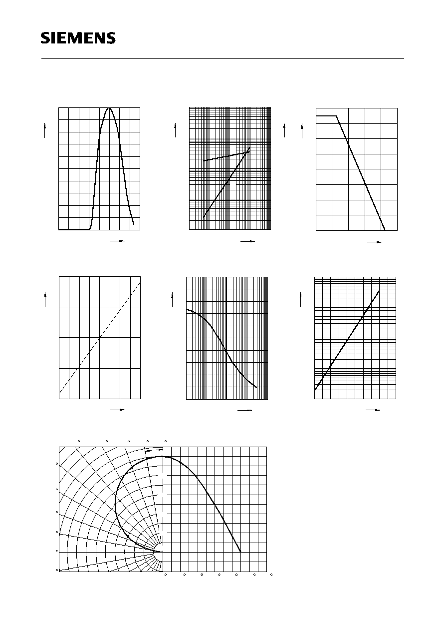
Fotoempfindlichkeit
Spectral sensitivity
V
R
= 5 V,
E
e
= 1 mW/cm
2
S
50 (
40)
µ
A
Wellenl‰nge der max. Fotoempfindlichkeit
Wavelength of max. sensitivity
S max
880
nm
Spektraler Bereich der Fotoempfindlichkeit
S
= 10 % von
S
max
Spectral range of sensitivity
S
= 10 % of
S
max
730 ... 1100
nm
Bestrahlungsempfindliche Fl‰che
Radiant sensitive area
A
7.00
mm
2
Abmessung der bestrahlungsempfindlichen
Fl‰che
Dimensions of radiant sensitive area
L
◊
B
L
◊
W
2.65
◊
2.65
mm
◊
mm
Halbwinkel
Half angle
±
60
Grad
deg.
Dunkelstrom,
V
R
= 10 V
Dark current
I
R
2 (
30)
nA
Spektrale Fotoempfindlichkeit
Spectral sensitivity
S
0.65
A/W
Quantenausbeute
Quantum yield
0.93
Electrons
Photon
Leerlaufspannung,
E
e
= 0.5 mW/cm
2
Open-circuit voltage
V
O
320 (
250)
mV

BPW 34 FA, BPW 34 FAS
BPW 34 FAS (E9087)
Semiconductor Group
4
1998-08-27
Kurzschluþstrom,
E
e
= 0.5 mW/cm
2
Short-circuit current
I
SC
23
µ
A
Anstiegs- und Abfallzeit des Fotostromes
Rise and fall time of the photocurrent
R
L
= 50
;
V
R
= 5 V;
= 850 nm;
I
p
= 800
µ
A
t
r
,
t
f
20
ns
Durchlaþspannung,
I
F
= 100 mA,
E
= 0
Forward voltage
V
F
1.3
V
Kapazit‰t,
V
R
= 0 V,
f
= 1 MHz,
E
= 0
Capacitance
C
0
72
pF
Temperaturkoeffizient von
V
O
Temperature coefficient of
V
O
TC
V
≠ 2.6
mV/K
Temperaturkoeffizient von
I
SC
Temperature coefficient of
I
SC
TC
I
0.03
%/K
Rausch‰quivalente Strahlungsleistung
Noise equivalent power
V
R
= 10 V
NEP
3.9
◊
10
≠ 14
W
Hz
Nachweisgrenze,
V
R
= 10 V,
Detection limit
D*
6.8
◊
10
12
cm ∑
Hz
W
Kennwerte (
T
A
= 25
∞
C,
= 870 nm)
Characteristics (cont'd)
Bezeichnung
Description
Symbol
Symbol
Wert
Value
Einheit
Unit