
Semiconductor Group
1
1998-09-15
Typ
Type
Emissions-
farbe
Color of
Emission
Farbe der
Lichtaustritts-
fl‰che
Color of the
Light Emitting
Area
Lichtst‰rke
Luminous
Intensity
I
F
= 20 mA
I
V
(mcd)
Lichtstrom
Luminous
Flux
I
F
= 20 mA
V
(mlm)
Bestellnummer
Ordering Code
LY R976-MO
LO R976-NO
LS R976-NO
yellow
orange
super-red
colorless clear
16 (30 typ.)
25 (55 typ.)
25 (55 (typ.)
250 (typ.)
450 (typ.)
450 (typ.)
Q62702-P5105
Q62702-P5101
Q62702-P5103
VEO06987
Besondere Merkmale
q
Geh‰usebauform: 0805
q
Industriestandard bzgl. Lˆtpadraster
q
geringe Bauteilhˆhe
q
f¸r IR-Lˆtung geeignet
q
f¸r Hinterleuchtungen und als opt. Indikator einsetzbar
q
gegurtet (8-mm-Filmgurt)
Features
q
0805 package
q
Industry standard footprint
q
low profile
q
suitable for IR reflow soldering process
q
for use as optical indicator and backlighting
q
available taped on reel (8 mm tape)
CHIPLED
LY R976, LO R976, LS R976

Semiconductor Group
2
1998-09-15
LY R976, LO R976
LS R976
Grenzwerte
Maximum Ratings
Bezeichnung
Parameter
Symbol
Symbol
Werte
Values
Einheit
Unit
Betriebstemperatur
Operating temperature range
T
op
≠ 30 ... + 85
∞C
Lagertemperatur
Storage temperature range
T
stg
≠ 40 ... + 85
∞C
Sperrschichttemperatur
Junction temperature
T
j
+ 95
∞C
Durchlaþstrom
Forward current
I
F
25
mA
Stoþstrom
Surge current
t
10
µ
s,
D
= 0.005
I
FM
0.1
A
Sperrspanung
Reverse voltage
V
R
3
V
Verlustleistung,
T
A
= 25 ∞C
Power dissipation,
T
A
= 25 ∞C
P
tot
70
mW
W‰rmewiderstand
Sperrschicht / Umgebung
Thermal resistance
Junction / air
R
th JA
700
K/W

Semiconductor Group
3
1998-09-15
LY R976, LO R976
LS R976
Kennwerte (
T
A
= 25 ∞C)
Characteristics
Bezeichnung
Parameter
Symbol
Symbol
Werte
Values
Einheit
Unit
LY
LO
LS
Wellenl‰nge des emittierten Lichtes
Wavelength at peak emission
I
F
= 20 mA
(typ.)
peak
591
610
645
nm
Dominantwellenl‰nge
Dominant wavelength
I
F
= 20 mA
(typ.)
dom
587
605
632
nm
Spektrale Bandbreite bei 50 %
I
rel max
Spectral bandwidth at 50 %
I
rel max
I
F
= 20 mA
(typ.)
15
16
16
nm
Abstrahlwinkel bei 50 %
I
v
(Vollwinkel)
Viewing angle at 50 %
I
v
2
160
160
160
Grad
deg.
Durchlaþspannung
Forward voltage
I
F
= 20 mA
(typ.)
I
F
= 20 mA
(max.)
V
F
V
F
2.0
2.6
2.0
2.6
2.0
2.6
V
V
Sperrstrom
Reverse current
(typ.)
V
R
= 3 V
(max.)
I
R
I
R
0.01
10
0.01
10
0.01
10
µ
A
µ
A
Temperaturkoeffizient von
peak
Temperature coefficient of
peak
I
F
= 20 mA
(typ.)
TC
peak
0.13
0.13
0.14
nm/K
Temperaturkoeffizient von
dom
,
Temperature coefficient of
dom
,
I
F
= 20 mA
(typ.)
TC
dom
0.10
0.07
0.01
nm/K
Temperaturkoeffizient von
V
F
,
Temperature coefficient of
V
F
,
I
F
= 20 mA
(typ.)
TC
V
F
≠ 2.5
≠ 1.7
≠ 2.0
mV/K

Semiconductor Group
4
1998-09-15
LY R976, LO R976
LS R976
Relative spektrale Emission
I
rel
=
f
(
),
T
A
= 25 ∞C,
I
F
= 20 mA
Relative spectral emission
V(
) =
spektrale Augenempfindlichkeit
Standard eye response curve
Abstrahlcharakteristik
I
rel
=
f
(
)
Radiation characteristic
OHL00415
350
0
20
40
60
80
100
nm
%
rel
V
yellow
orange
super-red
400
450
500
550
600
650
700
0
0.2
0.4
1.0
0.8
0.6
1.0
0.8
0.6
0.4
0∞
10∞
20∞
40∞
30∞
OHL00408
50∞
60∞
70∞
80∞
90∞
100∞
0∞
20∞
40∞
60∞
80∞
100∞
120∞

Semiconductor Group
5
1998-09-15
LY R976, LO R976
LS R976
Durchlaþstrom
I
F
=
f
(
V
F
)
Forward current
T
A
= 25 ∞C
Maximal zul‰ssiger Durchlaþstrom
Max. permissible forward current
I
F
=
f
(
T
A
)
Relative Lichtst‰rke
I
V
/
I
V(20 mA)
=
f
(
I
F
)
Relative luminous intensity
T
A
= 25 ∞C
Relative Lichtst‰rke
I
V
/
I
V(25 ∞C )
=
f
(
T
A
)
Relative luminous intensity
I
F
= 20 mA
V
OHL00232
F
F
10
-1
1.4
1.8
2.2
2.6
3.0 V 3.4
0
10
1
10
10
2
5
5
mA
5
1.0
OHL00420
0
0
∞C
mA
F
I
T
A
5
10
15
20
25
30
10 20 30 40 50 60 70 80
100
OHL00417
F
-1
10
V (20 mA)
10
-3
-2
-1
0
1
10
10
10
10
10
0
10
1
10
2
5
5
5
5
5
mA
V
super-red
yellow
orange
T
OHL00416
0
V (25 ∞C)
-20
0
20
40
60
∞C
100
A
0.4
0.8
1.2
1.6
2.0
V
yellow
orange
super-red
Semiconductor Group
6
1998-09-15
LY R976, LO R976
LS R976
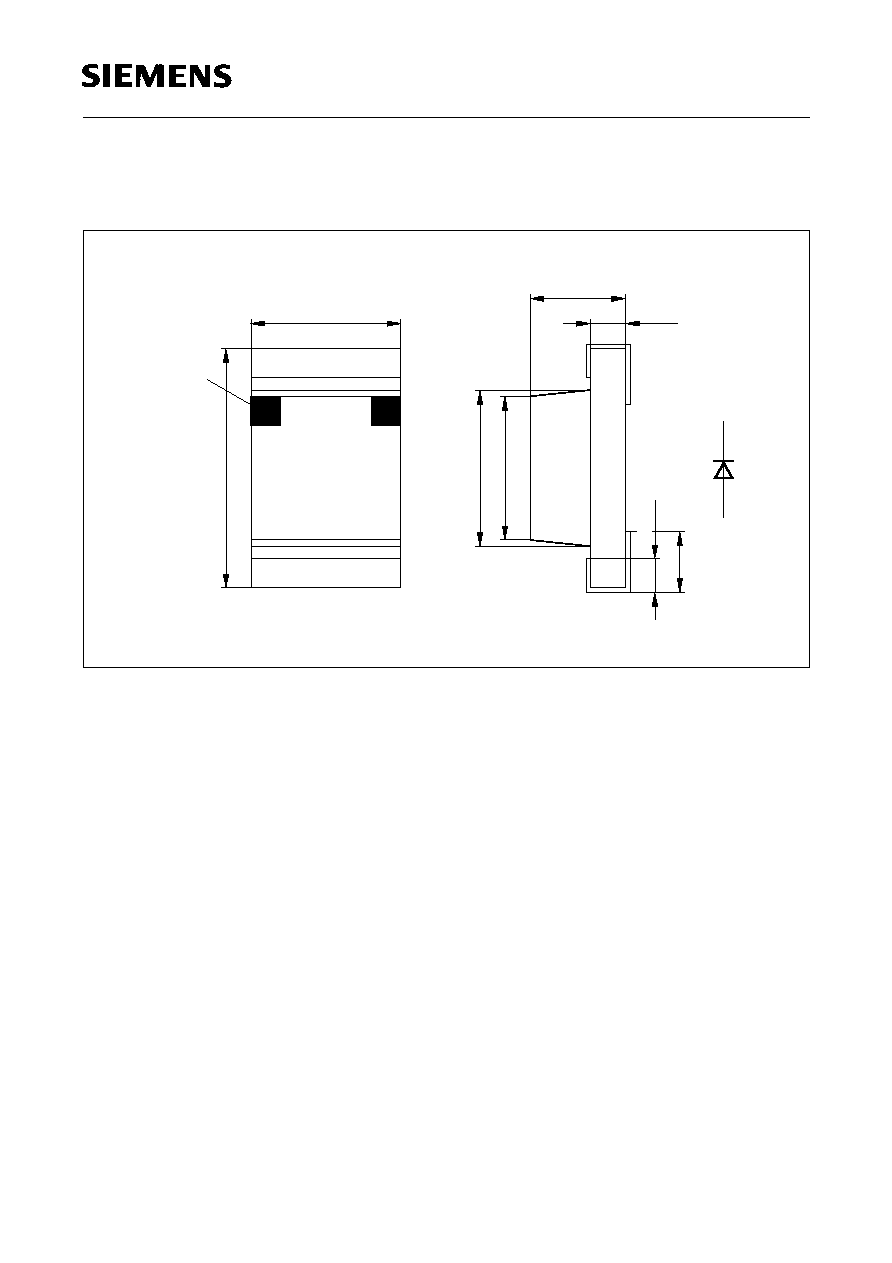
Maþzeichnung
(Maþe in mm, wenn nicht anders angegeben)
Package Outlines
(Dimensions in mm, unless otherwise specified)
GEO06987
1.25
±0.1
±0.1
2
Kathode/
1.2
±0.1
±0.1
1.3
±0.1
0.29
0.5
±0.1
±0.1
0.3
0.8
±0.1
Cathode
mark