Semiconductor Group
1
11.96
Besondere Merkmale
q
nicht eingef‰rbtes, teilweise diffuses Geh‰use
q
Lˆtspieþe im 2.54 mm Raster
q
Hohe Signalwirkung durch Farbwechsel der LED mˆglich
von gr¸n zu gelb und orange nach superrot
q
geeignet f¸r Multiplex- und Impulsbetrieb
q
beide Grundfarben gr¸n und rot getrennt ansteuerbar
q
Lˆtspieþe mit Aufsetzebene
q
gegurtet lieferbar
q
Stˆrimpulsfest nach DIN 40839
Features
q
partly diffused, colorless package
q
2.54 mm lead spacing
q
high signal efficiency by color change of the LED from
green to yellow and orange to superred
q
ideal for multiplexed or pulsed operations
q
both colors can be controlled separately
q
solder leads with stand-off
q
available taped on reel
q
load dump resistant acc. to DIN 40839
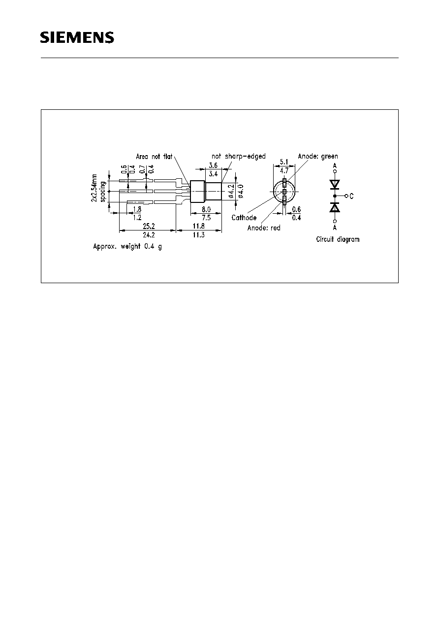
VEX06728
Streuung der Lichtst‰rke in einer Verpackungseinheit
I
V max
/
I
V min
2.0.
1)
Streuung der Lichtst‰rke in einer LED
I
V max
/
I
V min
4.0 (LU H371-FJ),
2.0 (LU H371-GK).
1)
Bei MULTILED
Æ
bestimmt die Helligkeit des jeweils dunkleren Chips in einem Geh‰use die Helligkeitsgruppe
der LED.
Luminous intensity ratio in one packaging unit
I
V max
/
I
V min
2.0.
1)
Luminous intensity ratio in one LED
I
V max
/
I
V min
4.0 (LU H371-FJ),
2.0 (LU H371-GK).
1)
In case of MULTILED
Æ
, the brightness of the darker chip in one package determines the brightness group of
the LED.
Typ
Type
Emissionsfarbe
Color of
Emission
Geh‰usefarbe
Color of
Package
Lichtst‰rke
Luminous
Intensity
I
F
= 10 mA
I
V
(mcd)
Bestellnummer
Ordering Code
LU H371-FJ
super-red / green
colorless clear
partly diffused
1.0 ... 8.0
Q62703-Q2050
LU H371-GK
super-red / green
1.6 ...12.5
Q62703-Q2051
Symbol MULTILED
Æ
5 mm (T1
3
/
4
), Partly Diffused
LU H371
Semiconductor Group
2
Grenzwerte
Maximum Ratings
1)
Bei gleichzeitigem Betrieb beider Dioden darf die Summe aus Strom und Verlustleistung die angegebene
Grenze nicht ¸berschreiten.
1)
With simultaneous operation of both diodes the sum of the current and the power dissipation must not exceed
the specified limits.
Bezeichnung
Parameter
Symbol
Symbol
Werte
Values
Einheit
Unit
Betriebstemperatur
Operating temperature range
T
op
≠ 55... + 100
∞C
Lagertemperatur
Storage temperature range
T
stg
≠ 55... + 100
∞C
Sperrschichttemperatur
Junction temperature
T
j
+ 100
∞C
Durchlaþstrom
Forward current
I
F
40
1)
mA
Stoþstrom
Surge current
t
10
µ
s,
D
= 0.005
I
FM
0.5
1)
A
Verlustleistung
Power dissipation
T
A
25∞C
P
tot
140
1)
mW
W‰rmewiderstand
Thermal resistence
Sperrschicht / Luft
Junction / air
R
th JA
400
K/W
LU H371
Semiconductor Group
3
Kennwerte (
T
A
= 25∞C)
Characteristics
Bezeichnung
Parameter
Symbol
Symbol
Werte
Values
Einheit
Unit
super-red
green
Wellenl‰nge des emittierten Lichtes
(typ.)
Wavelength at peak emission
(typ.)
I
F
=20 mA
peak
635
565
nm
Dominantwellenl‰nge
(typ.)
Dominant wavelength
(typ.)
I
F
=20 mA
dom
628
570
nm
Spektrale Bandbreite bei 50%
I
rel max
(typ.)
Spectral bandwidth at 50%
I
rel max
(typ.)
I
F
=20 mA
45
25
nm
Abstrahlwinkel bei 50%
I
v
(Vollwinkel)
Viewing angle at 50%
I
v
2
100
100
Grad
deg.
Durchlaþspannung
(typ.)
Forward voltage
(max.)
I
F
=10 mA
V
F
V
F
2.0
2.6
2.0
2.6
V
V
Kapazit‰t
(typ.)
Capacitance
V
R
= 0 V,
f
= 1 MHz
C
O
12
15
pF
Schaltzeiten:
Switching times:
I
V
from 10% to 90%
(typ.)
I
V
from 90% to 10%
(typ.)
I
F
= 100 mA,
t
p
= 10
µ
s,
R
L
= 50
t
r
t
f
300
50
450
200
ns
ns
LU H371

Semiconductor Group
5
Durchlaþstrom
I
F
=
f
(
V
F
)
Forward current
T
A
= 25∞C
Zul‰ssige Impulsbelastbarkeit
I
F
=
f
(
t
p
)
Permissible pulse handling capability
Duty cycle D = parameter,
T
A
= 25∞C
Relative Lichtst‰rke
I
V
/
I
V(10 mA)
=
f
(
I
F
)
Relative luminous intensity
T
A
= 25∞C
Maximal zul‰ssiger Durchlaþstrom
Max. permissible forward current
I
F
=
f
(
T
A
)
LU H371

Semiconductor Group
6
LU H371
Wellenl‰nge der Strahlung
peak
=
f
(
T
A
)
Wavelangth at peak emission
I
F
= 20 mA
Durchlaþspannung
V
F
=
f
(
T
A
)
Forward voltage
I
F
= 10 mA
Dominantwellenl‰nge
dom
=
f
(
T
A
)
Relative luminous intensity
I
F
= 20 mA
Relative Lichtst‰rke
I
V
/
I
V(25∞C )
=
f
(
T
A
)
Relative luminous intensity
I
F
= 10 mA