
Semiconductor Group
1
TBA 229-5
01.93
Type
Ordering Code
Package
TBA 229-5
Q67000-A5133
P-DIP-16
High AM suppression over a very wide
input voltage range
High sensitivity
Very high symmetry
Features
Dual Sound FM IF Amplifier
TBA 229-5
Bipolar IC
The component contains two separate FM sound IF sections for television stereo applications
or for multistandard receivers. Each FM section consists of an eight-stage symmetrical limiter
amplifier followed by a coincidence demodulator and an AF pre-amplifier with a low-ohmic
output. The component features considerably improved AM suppression characteristics with
small input signals, as well as a very low frequency deviation between
THD
min
and
AM
min
.
The component contains two separate limiter amplifiers with FM demodulators and separate
AF outputs.
Circuit Description
P-DIP-16

Semiconductor Group
2
TBA 229-5
Absolute Maximum Ratings
Parameter
Symbol
min.
max.
Unit
Limit Values
Supply voltage
V
S
0
16
V
Reference current
I
REF
0
2
mA
IF input voltage
V
I IF
rms
0
600
mV
DC voltages
V
9, 10, 11
V
14, 15, 16
0
0
V
REF
V
REF
V
V
DC currents
I
1, 2, 4, 5, 7, 8
0
2
mA
Junction temperature
T
j
150
�C
Storage temperature range
T
stg
� 40
125
�C
Thermal resistance (system-air)
R
th SA
80
K/W
Operating Range
Supply voltage
V
S
10.5
15.75
V
Ambient temperature
T
A
0
70
�C
Frequency
f
I
0.1
12
MHz

Semiconductor Group
3
TBA 229-5
Characteristics
V
S
= 12 V;
T
A
= 25 �C;
V
I IF 14
rms
= 10 mV;
f
I IF 11, 14
= 5.5 MHz;
f
mod
= 1 kHz;
f
=
�
30 kHz
(if not stated otherwise)
Parameter
Symbol
min. typ.
max.
Unit Test Condition
Limit Values
Current consumption
I
S
25
35
42
mA
Input voltage for
limiter threshold
V
I
11
rms
V
I 14
rms
50
50
100
100
�
V
�
V
V
Q 4, 5
= � 3 dB
Output voltage
V
Q 4
rms
V
Q 5
rms
510
510
600
600
700
700
mV
mV
DC voltage portion
V
Q 4
=
V
Q 5
=
4.8
4.8
6
6
6.2
6.2
V
V
f
= 0;
THD
=
THD
min
Total harmonic
distortion
THD
4
,THD
5
0.4
0.8
%
THD
=
THD
min
AM suppression
V
i rms
=1 mV;
m
= 30%
AM 4
AM 5
55
55
60
60
dB
dB
V
I
rms
=1 mV;
m
= 30%
Cross-talk rejection
C
IF 1-2
=
V
Q 4
/
V
Q 5
C
IF 1-2
=
V
Q 4
/
V
Q 5
60
60
dB
dB
f
I IF 11
= 5.5 MHz;
f
11
= 0 kHz;
V
I 11
rms
= 4 mV;
V
I 14
rms
=10 mV
f
I IF 11
= 5.74 MHz;
f
14
= 0 kHz
V
I 11
rms
= 4 mV;
V
I 14
rms
=10 mV
Reference voltage
V
13
=
5.4
6
6.6
V
Switching voltage
muting ON (AF off)
OFF
V
16
V
16
8
0
V
S
3
V
V
Design-Related Values
Input resistance
R
I 1, 2
R
I 7, 8
20
20
k
k
Output resistance
R
Q 4, 5
100
Input impedance
Z
I11, 14
800
IF residual voltage
V
Q 4, 5 (IF)
15
mV
Hum suppression
Q hum
32
dB
f
S
= 100 Hz
V
S
rms
= 500 mV;
V
S
/
V
Q 4
;
V
S
/
V
Q 5
Frequency deviation
AM
min
�
THD
min
f
IF
�
10
kHz

Semiconductor Group
4
TBA 229-5
Block Diagram
Semiconductor Group
5
TBA 229-5
Pin Functions
Pin No.
Function
1, 2
Demodulator tank circuit connection IF 1
(high impedance input � slope of S-curve can be determined by external resistor
between pins 1 and 2)
3
GND
4
AF output IF 1 (emitter follower)
5
AF output IF 2 (emitter follower)
6
Supply voltage
7, 8
Demodulator tank circuit connection IF 2
(high impedance input � slope of S-curve can be determined by external resistor
between pins 1 and 2)
9
Operating point feedback of limiter amplifier and low end IF 2
(RF decoupling of IF amplifiers with appropriate capacitors is required!
11
IF 2 input
(input of limiter amplifier IF 2; internal resistor between pins 9 and 11 is typ. 800
)
12
GND
13
Internal reference voltage (typ. 6 V)
14
IF 1 input
(input of limiter amplifier IF 2; internal resistor between pins 14 and 15 is
typ. 800
)
15
Operating feedback of limiter amplifier IF 1
(RF decoupling of IF amplifiers with appropriate capacitors is required!)
16
Operating point feedback of limiter amplifier and low end IF 1
(RF decoupling of IF amplifiers with appropriate capacitors is required!)
10
Operating point feedback of limiter amplifier IF 2
(RF decoupling of IF amplifiers with appropriate capacitors is required!)

Semiconductor Group
6
TBA 229-5
Diagrams
V
Q
:
THD
:
Measured at:
V
cct
:
Measured at:
Q
B
:
Measured at:
Circuit:
V
Q 4
rms
;
V
Q 5
rms
THD
4
;
THD
5
f
I IF
= 5.5 MHz;
f
= 30 kHz;
f
mod
= 1 kHz;
V
I IF
= 10 mV
V
1, 2
=
V
7, 8
f
I IF
= 5.5 MHz;
f
= 0 kHz;
V
I IF
= 10 mV
Q
between connections 1, 2 and 7, 8
f
I IF
= 5.5 MHz/
f
I IF
for 3 dB bandwidth,
f
= 0 kHz;
V
I IF
= 10 mV
L
= 10 turns 0.25 CuL; Vogt Coil Assembly 517 12 000 00 without cap
C
= 1 nF STYROFLEX Capacitor
AF Output Voltage, Total Harmonic Distortion,
Circuit Voltage versus Circuit
Q
B

Semiconductor Group
7
TBA 229-5
Tank Voltage versus
f
IF

Semiconductor Group
8
TBA 229-5
Tank Voltage versus
f
IF
Semiconductor Group
9
TBA 229-5
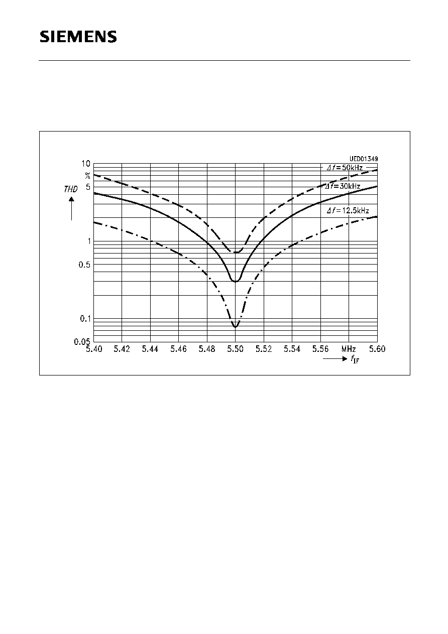
Total Harmonic Distortion versus Detuning (FM Operation)
THD
4
=
f
(
f
I IF
);
V
I
= 10 mV;
V
S
= 12 V;
f
mod
= 1 kHz,
f
= 50 kHz, 30 kHz, 12.5 kHz
Semiconductor Group
10
TBA 229-5
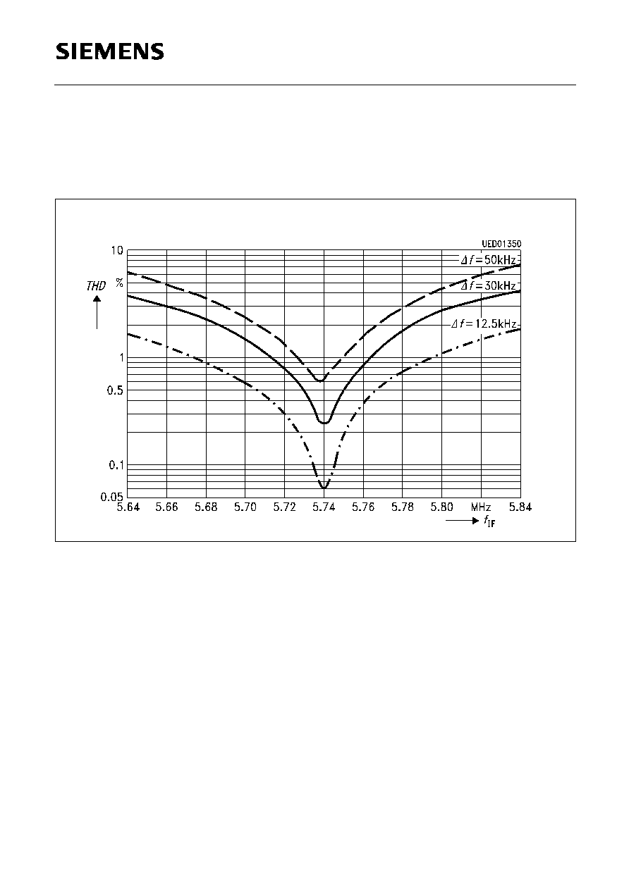
Total Harmonic Distortion versus Detuning (FM Operation)
compensated for minimum total harmonic distortion at
f
IF
= 5.5 MHz;
THD
=
f
(
f
I IF
);
V
I
= 10 mV;
V
S
= 12 V;
f
mod
= 1 kHz,
f
= 50 kHz; 30 kHz; 12.5 kHz
Semiconductor Group
11
TBA 229-5
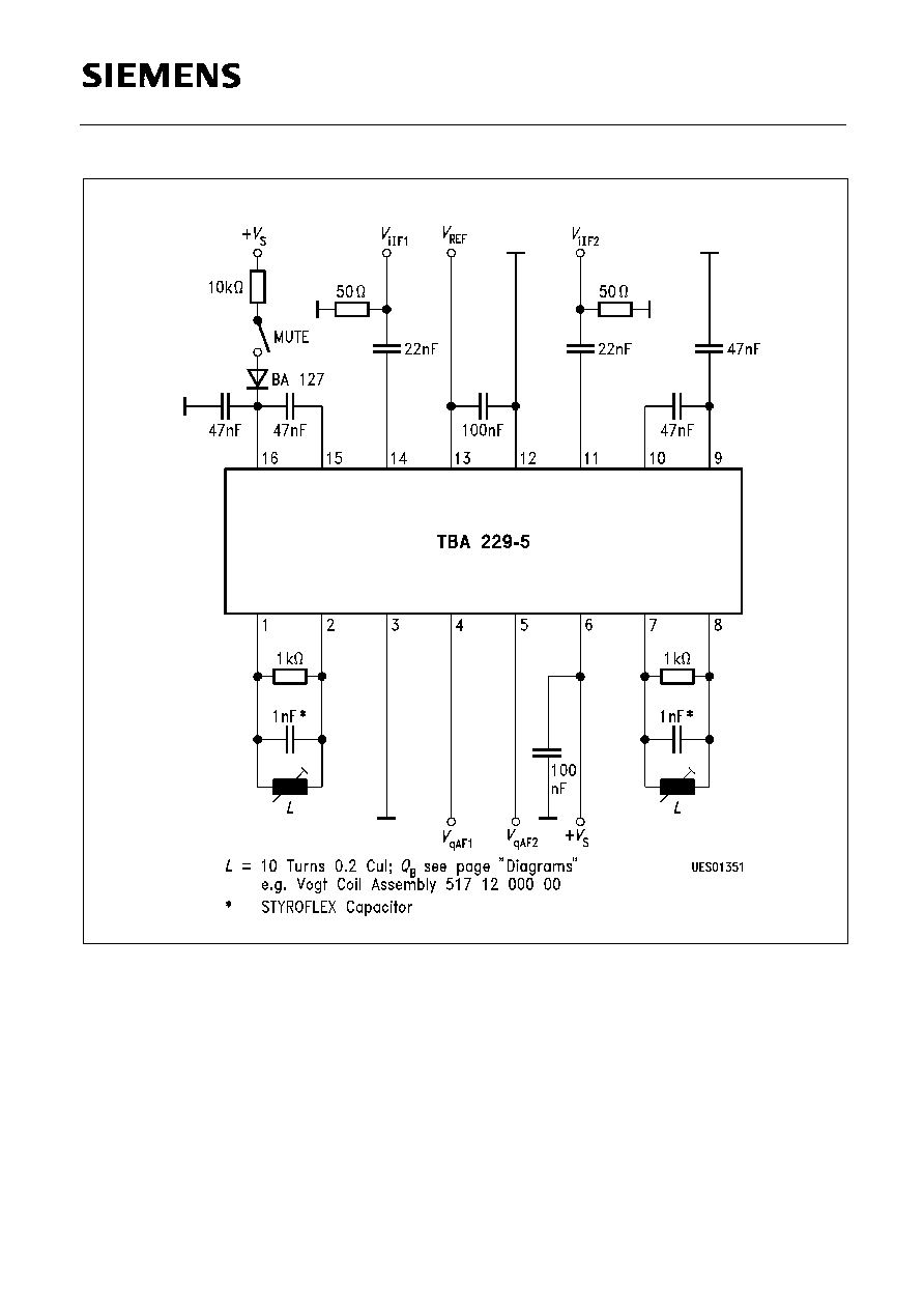
Test Circuit
Semiconductor Group
12
TBA 229-5
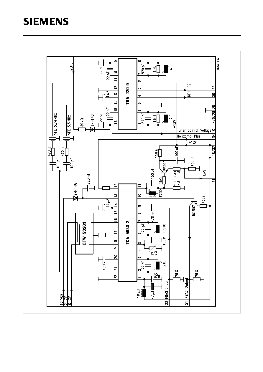
Application Circuit
L
= 10 turns 0.2 CuL;
Q
B
approx. 25
e.g. Vogt Coil Assembly 517 12 000 00