 | –≠–ª–µ–∫—Ç—Ä–æ–Ω–Ω—ã–π –∫–æ–º–ø–æ–Ω–µ–Ω—Ç: TCA2465G | –°–∫–∞—á–∞—Ç—å:  PDF PDF  ZIP ZIP |

Semiconductor Group
1
1998-02-01
Dual Power Operational Amplifier
Overview
Bipolar
IC
TCA 2465
Features
∑ High output peak current of twice 2.5 A
∑ Twice 2.0 A output peak current for TCA 2465 G
∑ Large supply voltage range up to 42 V
∑ High slew rate of 2 V/
µ
s
∑ Outputs fully protected (DC short-circuit proof for
P-SIP-9-1
V
S
up to 18 V;
for P-DSO-20-6
V
S
up to 14 V)
∑ Thermal overload protection
∑ Inhibit input enables "tristate" outputs
∑ Integrated clamp diodes
P-SIP-9-1
P-DSO-20-6
Description
The IC contains two identical op amps, each supplying a high output current of 2.5 A at
supply voltages between
±
3 V and
±
20 V. Internal compensation permits negative
feedback of the amplifiers up to a min. of 20 dB. Both amplifiers can be disconnected at
V
8
2 V via an inhibit input. Integrated protective circuits protect the outputs against
short-circuit to +
V
S
and ≠
V
S
and prevent thermal overloading of the IC. TCA 2465 G
comes in a special surface-mounted power package similar to P-DSO-20 and delivers
twice 2.0 A output peak current.
Type
Ordering Code
Package
TCA 2465
Q67000-A8109
P-SIP-9-1
TCA 2465 G
Q67000-A8334
P-DSO-20-6

TCA 2465
Semiconductor Group
2
1998-02-01
Figure 1
Pin Configuration (top view)
TCA 2465
9
1
Output 1
-Input 1
+Input 1
V
S
V
S
Inhibit Input
+Input 2
-Input 2
Output 2
-
+
IEP00550
TCA 2465 G
Output 2
Inhibit
IEP00888
13
14
10
15
9
16
8
17
7
18
6
19
5
20
4
3
2
1
V
S
11
12
N.C.
N.C.
Output 1
Inverting Input 1
Non-Inverting Input 1
Frequency Compensation 1
Inverting Input 2
Non-Inverting Input 2
Frequency Compensation 2
+
-
V
S
S
V
-
TCA 2465
Semiconductor Group
3
1998-02-01
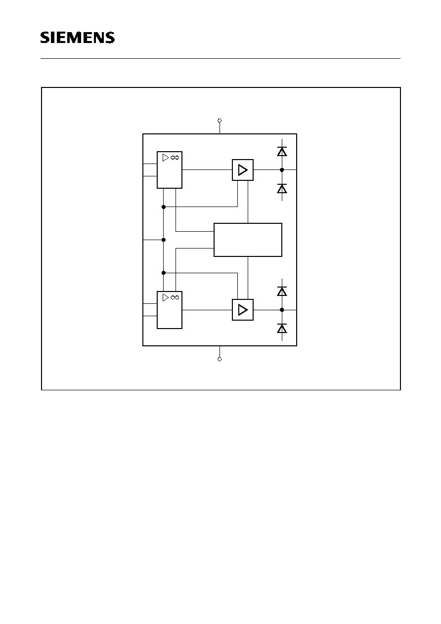
Figure 2
Block Diagram TCA 2465
IEB00551
Power Limitation
and
Thermal Protection
80 dB
0 dB
0 dB
80 dB
TCA 2465
3
2
8
7
6
+Input 1
Inhibit
Input
-Input 1
+Input 2
-Input 2
1
5
V
S
+
V
-
S
4
9
Output 1
Output 2
-
+
-
+

TCA 2465
Semiconductor Group
4
1998-02-01
Figure 3
Block Diagram TCA 2465 G
IEB00889
Power Limitation
and
Temperature Protection
80 dB
0 dB
0 dB
80 dB
TCA 2465 G
9
8
13
12
20
Inhibit
Inverting
2
1
V
S
+
V
-
S
4...7,14...17
19
Output 1
Output 2
10
11
Frequency
Compensation 1
Compensation 2
Frequency
Frequency
Compensation
Compensation
Frequency
Non-Inverting
Input 1
Non-Inverting
Inverting
Input 1
Input 2
Input 2
-
+
-
+

TCA 2465
Semiconductor Group
5
1998-02-01
1)
t
< 1 ms,
f
400 Hz
Absolute Maximum Ratings
T
C
= ≠ 40 to 85
∞
C
Note: Values in brackets refer to TCA 2465 G
Parameter
Symbol
Limit Values
Unit Remarks
min.
max.
Supply voltage
Differential input
voltage
V
S
V
ID
≠
≠
±
21
(≠
V
S
) + (
V
S
)
V
V
V
2-3
or
V
8-7
Output current
Output current
Supply current
Ground current
I
Q
I
Q
I
S
I
GND
≠ 2.5 (≠ 2)
1)
≠ 1.5
≠ 5 (≠ 2)
1)
≠ 5.5 (≠ 2)
1)
2.5 (2)
1)
≠
5.5 (2)
1)
5 (2)
1)
A
A
A
A
I
1
or
I
9
V
S
±
15 V;
V
Q
< ≠
V
S
I
S
I
4
Input voltage
Inhibit input
V
I
V
6
≠
V
S
≠
V
S
V
S
V
S
V
V
V
2
,
V
3
,
V
7
,
V
8
Junction temperature
Storage temperature
range
T
j
T
stg
≠
≠ 50
150
150
∞
C
∞
C
≠

TCA 2465
Semiconductor Group
6
1998-02-01
1)
P
D
= 12 W P-SIP-9-1
P
D
= 3.5 W P-DSO-20-6
Operating Range
Parameter
Symbol
Limit Values
Unit Remarks
min.
max.
Supply voltage
V
S
±
3
±
20
V
≠
Output current
I
Q
(≠ 1.3)
(1.3)
A
≠
Case temperature
T
C
≠ 40
85
∞
C
1)
Voltage gain
G
Vmin
20
≠
dB
≠
Forward current
I
F
of
free wheeling diodes
I
F
≠
(1.3)
A
≠
Thermal resistance
junction - ambient
junction - case
R
th jA
R
th jC
≠
≠
60
5
K/W
K/W
P-SIP-9-1
P-SIP-9-1
Thermal resistance
junction - ambient
junction - case
R
th jA
R
th jC
≠
≠
60
12
K/W
K/W
P-DIP-16-2
P-DIP-16-2
Thermal resistance
junction - ambient
junction - case
R
th jA
R
th jC
≠
≠
(70)
(22)
K/W
K/W
(soldered) P-DSO-20-6
P-DSO-20-6

TCA 2465
Semiconductor Group
7
1998-02-01
Characteristics
V
S
=
±
10 V;
T
j
= 25
∞
C, unless otherwise specified
Note: Values in brackets refer to TCA 2465; G
Parameter
Symbol
Limit Values
Unit
Test
Circuit
min.
typ.
max.
Open-loop supply current
consumption S1 in position 1
S1 in position 2
I
S
I
S
≠
≠
≠
30
5
50
mA
mA
1; 12
1; 12
Input offset voltage
V
IO
≠ 10
≠
10
mV
2; 13
Input offset current
Input current
I
IO
I
I
≠ 100
≠
≠
0.25
100
1
nA
µ
A
3; 14
3; 14
Output voltage
R
L
= 12
;
f
= 1 kHz
R
L
= 4
;
f
= 1 kHz
1)
R
L
= 470
;
f
= 40 kHz
V
Q pp
V
Q pp
V
Q pp
±
8.5
±
8
≠
±
9
±
8.5
±
8
≠
≠
≠
V
V
V
4; 15
4; 15
4; 15
Input resistance
f
= 1 kHz
R
I
1
5
≠
M
4; 15
Open-loop voltage gain
f
= 100 kHz
G
VO
70
80
≠
dB
5; 16
Common-mode input voltage
range
V
IC
7/≠ 10
±
7.5/≠ 10.5 ≠
V
6; 17
Common-mode rejection
Supply voltage rejection
k
CMR
k
SVR
70
≠ 70
80
≠ 80
≠
≠
dB
dB
6; 17
7; 18
Temperature coefficient of
V
IO
≠ 40
∞
C
T
j
+ 85
∞
C
Temperature coefficient of
I
IO
≠ 40
∞
C
T
j
+ 85
∞
C
VIO
IIO
≠
≠
50
0.4
≠
≠
µ
V/K
nA/K
2; 13
3; 14
Slew rate of
V
Q
for
non-inverting operation
Slew rate of
V
Q
for
inverting operation
SR
SR
≠
≠
2 (0.5)
2 (0.5)
≠
≠
V/
µ
s
V/
µ
s
8; 19
9; 20
Noise voltage
(DIN 45405, referred to input)
V
n
≠
3
≠
µ
V
1; 12
Inhibit input
(referred to ≠
V
S
)
V
6
for IC turned OFF
V
6
for IC turned ON
V
6 OFF
V
6 ON
2
≠
≠
≠
≠
0.8
V
V
1; 12
1; 12

TCA 2465
Semiconductor Group
8
1998-02-01
1)
Only for P-SIP-9-1
2)
Referred to ≠
V
S
3)
Switch S2 closed
4)
Only for P-SIP-9-1, for P-DSO-20-6
V
S
±
7 V
H-input current,
V
6
= 5 V
2)
L-input current,
V
6
= 0 V
2)
I
6H
I
6
≠
≠
0.1
0.5
0.5
3
µ
A
µ
A
1; 12
1; 12
Turn-ON dead time
I
I
1; 9
I > A
3)
referred to
Turn-OFF dead time
V
6 OFF/ON
I
I
1; 9
I < 1 A
3)
t
D ON
t
D OFF
≠
≠
10
10
20
20
µ
s
µ
s
1; 12
1; 12
Short-circuit current
4)
(switch S3 closed)
Short-circuit current
4)
(switch S4 closed)
I
SC
I
SC
≠
≠
1
1
≠
≠
A
A
1; 12
1; 12
Characteristics (cont'd)
V
S
=
±
10 V;
T
j
= 25
∞
C, unless otherwise specified
Note: Values in brackets refer to TCA 2465; G
Parameter
Symbol
Limit Values
Unit
Test
Circuit
min.
typ.
max.

TCA 2465
Semiconductor Group
9
1998-02-01
Test Circuits
Figure 4
Open-Loop Supply Current Consumption; Noise Voltage (TCA 2465 G)
Figure 5
Input Offset Voltage; Temperature Coefficient of
V
IO
(TCA 2465 G)
IES01367
+
-
11, 10
220 nF
1
20
10 k
100 k
10 k
13, 8
12, 9
1
19, 2
4
V
4
S
+
S1
V
-
S
IES01368
+
-
11, 10
220 nF
1
20
47
+
-
V
S
4.7 k
47
V
Q
V
S
V
Q
= 100
V
O

TCA 2465
Semiconductor Group
10
1998-02-01
Figure 6
Input Offset Current; Input Current; Temperature Coefficient of
I
IO
(TCA 2465 G)
Figure 7
Output Voltage; Input Resistance (TCA 2465 G)
IES01369
+
-
11, 10
220 nF
1
20
(220 pF)
+
-
V
S
V
Q
V
S
=
+
1 M
S2
47
1 M
S1
100
4.7 k
IES01370
+
-
11, 10
220 nF
1
20
+
-
V
S
V
Q
V
S
1 M
S
4.7 k
42.3 k
R
L
V
4.7 k
µ
10 F

TCA 2465
Semiconductor Group
11
1998-02-01
Figure 8
Open-Loop Voltage Gain
G
VO
(TCA 2465 G)
Figure 9
Common Mode Voltage Gain
G
VC
Common-Mode Rejection
k
CMR
(dB) =
G
VO
(dB) ≠
G
VC
(dB) (TCA 2465 G)
IES01371
+
-
11, 10
220 nF
1
20
8.2
~
~
+
-
V
Q
S
V
V
S
V
Q
= 20 x log (101 x
/
(
G
V0
V
( (
= 100 Hz
f
100 k
100
10
10 k
10 k
=
10 k
V
IES01372
+
-
11, 10
220 nF
1
20
8.2
~
~
+
-
V
Q
S
V
V
S
= 100 Hz
f
10
4.7 k
100
=

TCA 2465
Semiconductor Group
12
1998-02-01
Figure 10 Supply Voltage Rejection
k
SVR
(TCA 2465 G)
Figure 11 Slew Rate for Non-Inverting Operation (TCA 2465 G)
IES01373
+
-
11, 10
220 nF
1
20
8.2
~
~
220 nF
+
-
V
Q
S
V
V
S
47
470
k
SVR
(dB) = 20 x log
V
Q
(
/ (
G
V
V
S
x
( (
100 Hz
=
f
47
µ
1000 F
56
V
S
IES01374
+
-
11, 10
220 nF
1
20
8.2
10 k
~
~
(220 pF)
+
-
V
S
91 k
10 k
V
Q
Square-Wave
(Peak-to-Peak)
0.6 V
V
S

TCA 2465
Semiconductor Group
13
1998-02-01
Figure 12 Slew Rate for Inverting Operation (TCA 2465 G)
IES01375
+
-
11, 10
220 nF
1
20
8.2
~
~
(220 pF)
+
-
V
Q
S
V
V
S
10 k
100 k
Peak) 0.6 V
(Peak-to-
Square-Wave
10 k

TCA 2465
Semiconductor Group
14
1998-02-01
Figure 13 Non-Inverting Operation (TCA 2465 G)
IES01376
+
-
11, 10
220 nF
1
20
4.7 k
~
~
- 10 V
22 k
5.6 k
13, 8
1
19, 2
4
+ 10 V
12, 9
12
(220 pF)
IES01377
+
-
11, 10
220 nF
1
20
12
~
~
220 pF
- 10 V
13, 8
12, 9
1
19, 2
4
+ 10 V
a) Amplifier;
G
V
= 5
b) Voltage follower TCA 2465 G

TCA 2465
Semiconductor Group
15
1998-02-01
Figure 14 Inverting Operation (TCA 2465 G)
IES01378
+
-
1
11, 10
220 nF
1
75 k
4
20
19, 2
12
15 k
~
~
+ 10 V
- 10 V
12 k
12, 9
13, 8
IES01379
+
-
1
11, 10
220 nF
1
10 k
4
20
19, 2
12, 9
13, 8
12
10 k
~
~
220 pF
+ 10 V
10 V
- 10 V
a) Amplifier;
G
V
= ≠ 5
b) Inverter TCA 2465 G

TCA 2465
Semiconductor Group
16
1998-02-01
Figure 15 Open-Loop Supply Current Consumption; Noise Voltage (TCA 2465/A)
Figure 16 Input Offset Voltage; Temperature Coefficient of
V
IO
(TCA 2465/A)
IES00553
+
-
220 nF
1
10 k
100 k
10 k
4
V
4
S
+
S4
S2
S3
S1
V
-
S
1
2
2, 8
3, 7
1, 9
5
6
IES00554
+
-
220 nF
1
6
47
+
-
V
S
4.7 k
47
V
Q
V
S
V
Q
= 100
V
O

TCA 2465
Semiconductor Group
17
1998-02-01
Figure 17 Input Offset Current; Input Current; Temperature Coefficient of
I
IO
(TCA 2465)
Figure 18 Output Voltage; Input Resistance (TCA 2465)
IES00555
+
-
220 nF
1
6
+
-
V
S
V
Q
V
S
=
+
1 M
S2
47
1 M
S1
100
4.7 k
IES00556
+
-
220 nF
1
6
+
-
V
S
V
Q
V
S
1 M
S
k
4.7
42.3
k
R
L
V
4.7
k
µ
10 F

TCA 2465
Semiconductor Group
18
1998-02-01
Figure 19 Open-Loop Voltage Gain
G
VO
(TCA 2465)
Figure 20 Common Mode Voltage Gain
G
VC
Common-Mode Rejection
k
CMR
(dB) =
G
VO
(dB) ≠
G
VC
(dB) (TCA 2465/A)
IES00557
+
-
220 nF
1
6
8.2
~
~
+
-
V
Q
S
V
V
S
V
Q
= 20 x log (
/
(
G
V0
V
x
( (
= 100 Hz
f
101
100 k
100
10
10 k
10 k
=
10 k
V
IES00558
+
-
220 nF
1
6
8.2
~
~
+
-
V
Q
S
V
V
S
= 100 Hz
f
10
4.7 k
100
=

TCA 2465
Semiconductor Group
19
1998-02-01
Figure 21 Supply Voltage Rejection
k
SVR
(TCA 2465)
Figure 22 Slew Rate for Non-Inverting Operation (TCA 2465)
IES00559
+
-
220 nF
1
6
8.2
~
~
220 nF
+
-
V
Q
S
V
V
S
47
470
k
SVR
(dB) = 20 x log
V
Q
(
/ (
G
V
V
S
x
( (
= 100 Hz
f
47
µ
1000 F
56
V
S
IES00560
+
-
220 nF
1
6
8.2
10 k
~
~
+
-
V
S
91 k
10 k
V
Q
Square-Wave
(Peak-to-Peak)
0.6 V
V
S

TCA 2465
Semiconductor Group
20
1998-02-01
Figure 23 Slew Rate for Inverting Operation (TCA 2465)
Note: Values in brackets refer to TCA 2465 A
Figure 24 Non-Inverting Operation (TCA 2465)
IES00561
+
-
220 nF
1
6
8.2
~
~
+
-
V
Q
S
V
V
S
10 k
100 k
Peak) 0.6 V
(Peak-to-
Square-Wave
10 k
IES00562
+
-
220 nF
1
4.7 k
~
~
22 k
5.6 k
+10 V
-10 V
4
2, 8
3, 7
6
4
1, 9
5
Amplifier;
G
V
= 5

TCA 2465
Semiconductor Group
21
1998-02-01
Figure 25 Inverting Operation (TCA 2465)
IES00564
+
-
5
220 nF
1
75 k
4
6
1, 9
3, 7
4
15 k
~
~
+10 V
-10 V
12 k
2, 8
Amplifier;
G
V
= ≠ 5

Semiconductor Group
22
1996-05-01
TCA 2465
Safe Operating Area (SOA) Peak Output
Current versus Collector-Emitter Voltage
T
j
= 25
∞
C,
V
CE
= +
V
S
≠
V
Q
or
V
CE
= ≠
V
S
≠
V
Q
Supply Current versus
Supply Voltage
T
j
= 25
∞
C
Max. Permissible Power Dissipation versus
Case Temperature
Input Current versus
Junction Temperature
V
S
=
±
10 V
IED00576
0
0
V
CE
Q
0.5
1.0
1.5
2.0
2.5
3.0
3.5
4.0
A
10
20
30
40 V 50
IED00567
0
0
V
S
S
5
10
15
20 V 25
10
20
30
40
mA
50
IED00566
0
0
P
tot
T
C
TCA 2465G
4
8
12
16
20
24
25
50
75
100
∞C
150
W
TCA 2465
IED00568
100
-40
150
200
250
nA
300
∞C
-25
0
25
50
75
T
j

Semiconductor Group
23
1996-05-01
TCA 2465
Open-Loop Voltage Gain versus
Frequency
TCA 2465, G Open-Loop Voltage Gain
versus Frequency
V
S
=
±
10 V,
T
j
= 25
∞
C
Phase Response versus Frequency
V
S
=
±
10 V;
T
j
= 25
∞
C
TCA 2465, G Phase Response
versus Frequency
V
S
=
±
10 V,
T
j
= 25
∞
C
IED00569
0
f
VO
G
10
20
30
40
50
60
70
80
dB
100
10
1
10
2
10
3
10
4
10
5
10
6
Hz
V
S
= ±10 V
25
=
∞C
T
j
IED00571
0
f
VO
G
10
20
30
40
50
60
70
80
dB
100
10
1
10
2
10
3
10
4
10
5
10
6
Hz
C
comp
= 220 pF
= 100 pF
comp
C
C
comp
= 0 pF
IED00570
-180
f
-
10
1
-150
-120
-90
-60
-30
Deg.
0
2
10
3
10
4
10
5
10
6
10
7
10
Hz
IED00570
-180
f
-
10
1
-150
-120
-90
-60
-30
Deg.
0
2
10
3
10
4
10
5
10
6
10
7
10
Hz

Semiconductor Group
24
1996-05-01
TCA 2465
Common-Mode Rejection versus
Case Temperature
V
S
=
±
10 V
Forward Current versus
Forward Voltage
Saturation Voltage versus
Peak Output Current
T
j
= 25
∞
C
IED00573
70
-40
T
CMR
k
75
80
85
dB
90
∞C
-25
0
25
50
75
C
IED00575
0
0
F
V
F
= 25 ∞C
1.0
V
2.0
1.0
2.0
A
3.0
Pin (9) 5
Pins (7, 10) 1, 9
Pins 1, 9
Pin 4
TCA 2465
TCA 2465G
T
j
IED00574
0
0
V
Sat
Q
= 25 ∞C
TCA 2465G
0.5
1.0
1.5
2.0 A 2.5
0.5
1.0
1.5
V
2.0
TCA 2465
T
j

TCA 2465
Semiconductor Group
25
1998-02-01
Package Outlines
P-SIP-9-1
(Plastic Single In-line Package)
GPI
0
5
038
Sorts of Packing
Package outlines for tubes, trays etc. are contained in our
Data Book "Package Information".
Dimensions in mm

TCA 2465
Semiconductor Group
26
1998-02-01
1
10
11
20
Index Marking
1) Does not include plastic or metal protrusions of 0.15 max per side
2) Does not include dambar protrusion of 0.05 max per side
GPS05094
2.65 max
0.1
0.2
-0.1
2.45
-0.2
+0.15
0.35
1.27
2)
0.2 24x
-0.2
7.6
1)
0.35 x 45∞
0.23
8∞ max
+0.09
+0.8
±0.3
10.3
0.4
12.8
-0.2
1)
P-DSO-20-6
(Plastic Dual Small Outline Package)
Sorts of Packing
Package outlines for tubes, trays etc. are contained in our
Data Book "Package Information".
Dimensions in mm
SMD = Surface Mounted Device