 | –≠–ª–µ–∫—Ç—Ä–æ–Ω–Ω—ã–π –∫–æ–º–ø–æ–Ω–µ–Ω—Ç: TDA4916GG | –°–∫–∞—á–∞—Ç—å:  PDF PDF  ZIP ZIP |
P-DSO-24-1
Semiconductor Group
1
05.96
SMPS-IC with MOSFET Driver Output
TDA 4916 GG
Features
∑ High clock frequency
∑ Low current drain
∑ High reference accuracy
∑ All monitoring functions
Functional Description and Application
The general-purpose single-ended switch-mode power supply device for the direct
control of SIPMOS power transistors incorporates both digital and analog functions.
These are required for the construction of high-quality flyback, forward and choke
converters. The device can be likewise used for transformer-less voltage multipliers and
variable-speed motors.
Faults occurring during operation of the switch-mode power supply are detected by
comparators integrated in the device which initiate protective functions.
In addition, pairs of power supplies can be synchronized in antiphase. In-phase or
antiphase synchronization is possible when more than two power supplies are involved.
Type
Ordering Code
Package
TDA 4916 GG
Q67000-A9230
P-DSO-24-1
TDA 4916 GG
Semiconductor Group
2
05.96
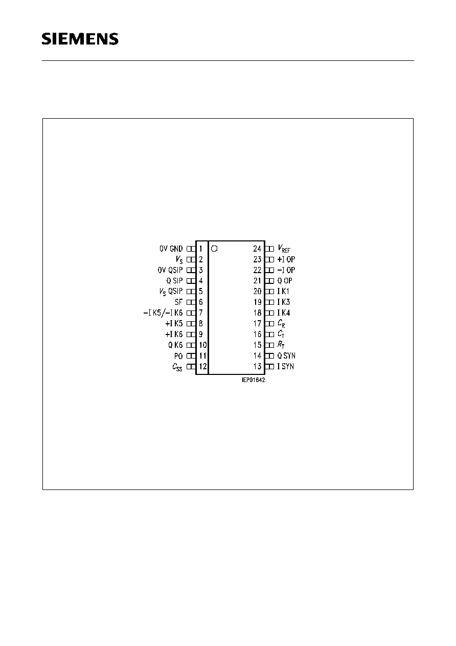
Pin Configuration
(top view)
Figure 1
P-DSO-24-1
TDA 4916 GG
Semiconductor Group
3
05.96
Pin Definitions and Functions
Pin No.
Symbol
Function
1
0V GND
GND
2
V
S
Supply voltage
3
0V QSIP
Ground QSIP
4
Q SIP
SIPMOS driver
5
V
S
QSIP
Supply voltage driver
6
SF
Series feed
7
≠ I K5/≠ I K6
Current sensor negative input
8
+ I K5
Current sensor K5
9
+ I K6
Current turn-OFF K6
10
Q K6
Output K6
11
PO
Pulse omission
12
C
SS
Soft start
13
I SYN
Input synchronization
14
Q SYN
Output synchronization
15
R
T
Frequency generator
16
C
T
Frequency generator
17
C
R
Ramp generator
18
I K4
Input undervoltage
19
I K3
Input overvoltage
20
I K1
Input K1
21
Q OP
Output operational amplifier
22
≠ I OP
Input operational amplifier
23
+ I OP
Input operational amplifier
24
V
REF
Reference voltage
TDA 4916 GG
Semiconductor Group
4
05.96
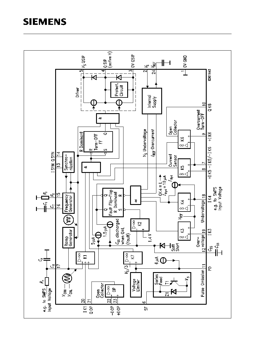
Figure 2
Block Diagram

TDA 4916 GG
Semiconductor Group
5
05.96
Circuit Description
The individual functional sections of the device and their interactions are described
below.
Power Supply at
V
S
The device does not enable the output until the turn-ON threshold of
V
S
is exceeded. The
duty factor (active time/period) can then rise from zero to the value set with K1 in the time
determined by the soft start. The turn-OFF threshold lies below the turn-ON threshold.
Below the turn-OFF threshold the output Q SIP is reliably low.
Frequency Generator
The frequency is mainly determined by close-tolerance external components and the
calibrated reference voltage.
The switching frequency at the output can be set by suitable choice of
R
t
and
C
t
.
The maximum possible duty factor can be reduced by a defined amount by means of a
resistor from
C
T
to 0V GND. The maximum possible duty factor can be increased by a
defined amount by means of a resistor from
C
T
to
V
S
.
Ramp Generator
The ramp generator is controlled by the frequency generator and operates with the same
frequency. Capacitor
C
r
on the ramp generator is discharged by an internally-set current
and charged via a current set externally. The duration of the falling edge of the ramp
generator output must be shorter than its rise time. Only then do the upper and lower
switching levels of the ramp generator signal have their nominal values.
In "voltage mode control" operation, the rising edge of the ramp generator signal is
compared with an externally set dc voltage in comparator K1 for pulse-width control at
the output. The slope of the rising edge is set by the current through
R
r
. The voltage
source connected to
R
r
can be the SMPS input voltage. This makes it possible to control
the duty factor for a constant volt-second product at the output. This control option
(precontrol) permits equalization of known disturbances (e.g. input voltage ripple).
Superimposed load current control (current mode control) can also be implemented. For
this purpose the actual current at the source of the SIPMOS transistor is sensed and
compared with the specified value in comparator K5.

TDA 4916 GG
Semiconductor Group
6
05.96
Comparator K1 (duty factor setting for voltage mode control)
The two plus inputs of the comparator are so connected that the lower plus level is
always compared with the minus input level. As soon as the voltage of the rising edge of
the sawtooth (minus input) exceeds the lower of the two plus input levels, the output is
inhibited via the turn-OFF Flip-Flop, that is to say the High time of the output can be
continuously varied. Since the frequency remains constant, this corresponds to a duty
factor change.
Comparator K2
The comparator has a switching threshold at 1.5 V. Its output sets the fault Flip-Flop
when the voltage on capacitor
C
a
lies below 1.5 V. However, the fault Flip-Flop accepts
the setting pulse only if no reset pulse (fault) is applied. This prevents resetting of the
output as long as a fault signal is present.
Comparators K3 (overvoltage), K4 (undervoltage),
V
S
Undervoltage,
V
REF
Overcurrent
These are fault detectors which cause the output to be inhibited immediately by the fault
Flip-Flop when faults occur. When faults are no longer present, the duty factor is
reestablished via the soft start
C
SS
. In the event of undervoltage, a current is injected at
the input of K4 with the aid of which an adjustable hysteresis or latching is made
possible. The value of the hysteresis is determined by the internal resistance of the
external drive source and the current injected internally at the input of K4. In the event
of undervoltage at K4, the injected current flows into the device.
Comparator K5 (duty factor setting for current mode control)
K5 is used to sense the source current at the switching transistor. The plus input of the
comparator is fed out. Enabling of output Q SIP after cessation of the fault is effected
with an H signal at the turn-OFF Flip-Flop output.
Comparator K6 (overcurrent turn-OFF)
The turn-OFF Flip-Flop is reset when overcurrent is detected by K6. In combination with
the pulse-omission facility, individual pulses can then be omitted. This then results in a
limited rise in the output current with a rising overload at the output.

TDA 4916 GG
Semiconductor Group
7
05.96
Operational Amplifier OP
Opamp OP is a high-quality operational amplifier. It can be used in the control circuit to
transfer the variations in the voltage to be regulated in amplified form to the free plus
input of comparator K1. As a result, a voltage change is converted into a duty factor
change. The output of OP is an open collector. The frequency response of OP is already
corrected. The plus input is connected internally via a capacitor to ground. This gives the
inverting amplifier a more favorable phase response.
Turn-OFF Flip-Flop AFF
A pulse is fed to the set input of the turn-OFF Flip-Flop with the falling edge of the
frequency generator signal. However, it can only really be set if no reset signal is applied.
With a set turn-OFF Flip-Flop, the output is enabled and can be active. The Flip-Flop
inhibits the output in the event of a turn-OFF signal from K1, K5, K6 or K7.
Fault Flip-Flop
Fault signals fed to the reset input of the fault Flip-Flop cause the output to be
immediately disabled (Low), and to be turned on again via the soft start
C
SS
after
removing fault-condition.
Soft Start
C
SS
The smaller of the two voltages at the plus inputs of K1 - compared with the ramp
generator voltage - is a measure of the duty factor at the output. At the instant the device
is turned-ON, the voltage on capacitor
C
SS
equals zero. Provided no fault exists, the
capacitor is charged up to its maximum value.
C
SS
is discharged in the event of a fault. However, the fault Flip-Flop inhibits the output
immediately. Below a charging voltage of approx. 1.5 V, a set signal is applied to the fault
Flip-Flop and the output is enabled, provided a reset signal is not applied
simultaneously. However, since the minimum ramp generator voltage is about 1.8 V, the
duty factor at the output is not actually slowly and continuously increased until the
voltage on
C
SS
exceeds a value of 1.8 V.
The Z-diode limits the voltage on capacitor
C
SS
. The voltage at the ramp generator can
reach a higher level than the Zener voltage. With a suitable ramp generator rising edge
slope, the duty factor can be limited to a wanted maximum value.
Pulse Omission PO
In the event of overcurrent in the SIPMOS transistors it is frequently necessary to omit
pulses even with minimum duty factor. Only this measure ensures that the SIPMOS
transistors cannot be overloaded. This wanted function can be achieved with Pulse
Omission PO and Overcurrent Comparator K7 by means of a suitable external circuit.

TDA 4916 GG
Semiconductor Group
8
05.96
Reference Voltage
V
REF
The reference voltage source makes available a source with a high-stability temperature
characteristic which can be used for external connection to the operational amplifier, the
fault comparators, the frequency generator, or to other external units. The voltage
source is short-circuit-proof to ground.
Synchronization I SYN, Q SYN
The device has an input and an output for synchronization. In the case of a synchronized
device (slave), its output Q SIP is in phase opposition to the output Q SIP of the
synchronizing device (master). In the case of an unconnected input I SYN, or with
connection to
V
REF
, or also when a series capacitor (without switching transitions) is
connected, the device receives its clock from the internal frequency generator in
accordance with the circuit connected to it. As soon as switching transitions appear at
I SYN, switchover to external synchronization and vice versa takes place after a delay.
After a switchover process, a few clock cycles must elapse in addition to the delay before
the frequency and phase achieve their steady states.
Series Feed SF
The Series Feed circuit section is used to turn-OFF the external series-feed transistor
when energy recovery commences. As a result there is minimum power loss in the
supply to the device. With the series-feed transistor turned-OFF, its drive current flows
via VS to
V
S
.
SIPMOS Driver Output Q SIP
The output is High active. The time during which the output is active can be continuously
varied.
The duration of the rising edge of the frequency generator signal is the minimum time
during which the output can be Low.
The duration of the falling edge of the frequency generator signal is the maximum time
during which the output can be High.
The output driver is designed as a push-pull stage. The output current is limited internally
to the specified values.
Output Q SIP is connected via diodes to the supply
V
S
QSIP and 0V QSIP.
A protection circuit SS lies between Q SIP and GND to clamp the output to ground at low
impedance in the event of undervoltage at
V
S
.

TDA 4916 GG
Semiconductor Group
9
05.96
When the supply to the switch-mode power supply is switched on, the capacitive
displacement current from the gate of the SIPMOS transistor is conducted to the
smoothing capacitor at
V
S
QSIP by the diode connected to
V
S
QSIP. The voltage at
V
S
QSIP may reach about 2.3 V in the process without the SIPMOS transistor being
turned-ON.
The diode connected to ground clamps negative voltages at Q SIP to minus 0.7 V.
Capacitive currents which occur with voltage dips at the drain terminal of the SIPMOS
transistor can then flow away unimpeded.
The output is active Low with supply voltages at
V
S
and
V
S
QSIP from about 4 V on. The
function of the diode connected to
V
S
QSIP and the resistor are then taken over by the
pull-down source.
The two ground terminals 0V SQIP and 0V GND can lie at different levels. This permits
connections to be made to the SIPMOS transistor in such a way that the drive currents
for the gate do not flow to the source via the current-sensing resistor. The maximum
permissible level differences between 0V GND and 0V SQIP are given under Functional
Range. If greater level differences are anticipated, it is better to join the two terminals.
TDA 4916 GG
Semiconductor Group
10
05.96
Absolute Maximum Ratings
T
A
= ≠ 40 to 85
∞
C
Parameter
Symbol
Limit Values Unit
Test Condition
min.
max.
Supply voltage;
V
S
,
V
S QSIP
I OP, I K1, I K3, I K4, I K5, I K6,
I SYN
Q SYN
V
S
,
V
VS QSIP
V
I
V
I SYN
I
I SYN
V
Q SYN
≠ 0.3
≠ 0.3
0
≠ 3
≠ 0.3
17
17
5
3
5
V
V
V
mA
V
V
I SYN
> 5 V or
V
I SYN
< 0 V
Frequency Generator;
C
T
,
R
T
V
CT, RT
I
CT, RT
≠ 0.3
0
5
3
V
mA
V
CT
> 5 V
Ramp Generator;
C
R
V
CR
I
CR
≠ 0.3
0
V
CRH
3
V
mA
V
CRH
(see charact.)
V
CR
>
V
CRH
Reference voltage;
V
REF
V
REF
I
REF
≠ 0.3
≠ 10
6
10
V
mA
V
REF
> 6 V or
V
REF
< ≠ 0.3 V
Output Opamp; Q OP
Inhibited
Conducting
V
Q OP
I
Q OP
≠ 0.3
0
17
5
V
mA
Output Overcurrent Turn-OFF;
Q K6
Inhibited
Conducting
V
Q K6
I
Q K6
≠ 0.3
0
17
5
V
mA
Driver output; Q SIP
V
Q SIP
≠ 0.3
V
S
V
1)
Q SIP clamping diodes
I
Q SIP
≠ 10
10
mA
V
Q SIP
>
V
S
or
V
Q SIP
< ≠ 0.3 V
Soft start;
C
SS
V
CSS
I
CSS
≠ 0.3
0
V
SSH
100
V
µ
A
V
SSH
(see charact.)
V
SS
>
V
SSH
Pulse omission; PO
V
PO
I
PO
≠ 0.3
0
V
POH
3
V
mA
V
POH
(see charact.)
V
PO
>
V
POH
Series feed; SF
V
SF
≠ 0.3
17
V
Junction temperature
T
j
≠ 65
150
∞
C
Storage temperature
T
s
≠ 65
150
∞
C
Thermal resistance
system - ambient
R
th S/A
60
K/W
The values refer to the two connected ground terminals.
1) Important: observe max. power loss or junction temperature.

TDA 4916 GG
Semiconductor Group
11
05.96
Operating Range
Function
Symbol
Limit Values
Unit
min.
max.
Supply voltage
V
S
V
VS QSIP
0
0
15
15
V
V
Frequency generator
f
0.05
400
kHz
Ramp generator
f
0.05
400
kHz
Ambient temperature
T
A
≠ 40
+ 100
∞
C
Ground Q SIP
V
0V QSIP
GND ≠ 300 mV
GND + 2 V
V
Resistor at
R
T
R
RT
27
1000
k
Characteristics
V
Son
<
V
S
< 15 V, ≠ 25
∞
C <
T
A
< 85
∞
C;
V
Son
means that
V
S
has exceeded
V
SH
, but has
not gone below
V
SL
.
Parameter
Symbol
Limit Values
Unit
Test Condition
min.
typ.
max.
Current in
V
S
I
VS
7
8
mA
1)
mA
1)
FG at 100 kHz
FG at 300 kHz
Q SYN
unconnected
8
9
mA
1)
mA
1)
FG at 100 kHz
FG at 300 kHz
Q SYN to 0V GND
Current in
V
S
QSIP
I
VS QSIP
2.5
5.5
mA
1)
mA
1)
FG at 100 kHz
FG at 300 kHz
Current in
V
S
+
V
S
QSIP
I
Sum
9
13
mA
1)
mA
1)
FG at 100 kHz
FG at 300 kHz
Q SYN
unconnected
10
14
mA
1)
mA
1)
FG at 100 kHz
FG at 300 kHz
Q SYN to 0 V GND

TDA 4916 GG
Semiconductor Group
12
05.96
Current Drain
2)
Hysteresis at
V
S
Turn-ON threshold
for
V
S
rising
Turn-OFF threshold
for
V
S
falling
V
SH
V
SL
8.0
7.9
9.1
9.0
10
9.9
V
V
1)
C
T
;
R
T
(see oscillator nomogram).
2)
The currents as
V
S
and
V
S
QSIP are in each case without loads and without internal discharge to
C
R
, as well
as with active output Q SIP.
Reference Voltage
Voltage
Load current
V
REF
≠
I
REF
2.460
0
2.500
2.540
3
V
mA
I
REF
= 250
µ
A;
V
S
= 12 V
V
REF
< 30 mV
Voltage change
Voltage change
V
REF
V
REF
5
3
mV
mV
0 mA <
I
REF
< 500
µ
A
12 V <
V
S
< 14 V
Temperature
response
Operate threshold
V
REF
overcurrent
V
REF
/
T
≠
I
REFO
3
0.1
6
10
mV/K
mA
Frequency Generator
Nominal frequency
spread
f
F
/
f
O
≠ 4
4
%
20 kHz <
f
O
< 150 kHz;
Q SYN to GND;
V
S
= 12 V;
T
A
= 25
∞
C
Voltage dependence
of nominal
frequency
f
V
/
f
O
≠ 1
1
%
10 V <
V
S
< 14.4 V;
T
A
= 25
∞
C;
relative to
f
O
at 12 V;
20 kHz <
f
O
< 150 kHz
Characteristics (cont'd)
V
Son
<
V
S
< 15 V, ≠ 25
∞
C <
T
A
< 85
∞
C;
V
Son
means that
V
S
has exceeded
V
SH
, but has
not gone below
V
SL
.
Parameter
Symbol
Limit Values
Unit
Test Condition
min.
typ.
max.
TDA 4916 GG
Semiconductor Group
13
05.96
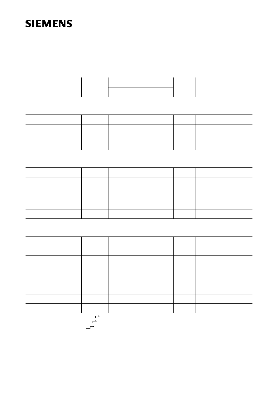
Temperature-
dependence of
nominal frequency
f
/
f
O
≠ 3
3
%
≠ 25
∞
C <
T
A
< + 85
∞
C;
V
S
= 12 V;
relative to
f
O
at 25
∞
C;
20 kHz <
f
O
< 150 kHz
Nominal frequency
f
20150
0.92
f
O
f
O
1.08
f
O
kHz
1)
20 kHz to 150 kHz
Nominal frequency
f
150250
0.88
f
O
f
O
1.12
f
O
kHz
1),2)
150 kHz to 250 kHz
Nominal frequency
f
250300
0.85
f
O
f
O
1.15
f
O
kHz
1),2)
250 kHz to 300 kHz
Maximum duty cycle
20150
48
52
%
2)
20 kHz to 150 kHz
Maximum duty cycle
150200
46
54
%
2)
150 kHz to 250 kHz
Maximum duty cycle
250300
44
56
%
2)
250 kHz to 300 kHz
Ramp Generator
Frequency range
f
0.05
300
kHz
Maximum voltage at
C
R
V
CRH
4.8
5.8
6.8
V
Minimum voltage
at
C
R
V
CRL
1.4
1.8
2.2
V
Discharge current at
C
R
I
dis
0.75
1.00
1.25
mA
internally fixed
Capacitance at
C
R
C
R
10
pF
ON-time spread
(limited by
C
SS
)
t
Ot
/
t
Ot
≠ 9
9
%
C
r
= 200 pF;
V
IK1
>
V
SSH
;
I
Rr
= 150
µ
A;
T
A
= 25
∞
C;
relative to
t
Ot
= 4.0
µ
s
1)
C
T
;
R
T
(see oscillator nomogram).
2)
See diagram: Tolerance of oscillator frequency, duty cycle.
Characteristics (cont'd)
V
Son
<
V
S
< 15 V, ≠ 25
∞
C <
T
A
< 85
∞
C;
V
Son
means that
V
S
has exceeded
V
SH
, but has
not gone below
V
SL
.
Parameter
Symbol
Limit Values
Unit
Test Condition
min.
typ.
max.
TDA 4916 GG
Semiconductor Group
14
05.96
ON-time drift
t
Ot
/
t
Ot
≠ 2
2
%
C
r
= 200 pF;
V
IK1
>
V
CAH
;
I
Rr
= 150
µ
A;
relative to
t
Ot
= 25
∞
C
ON-time spread
t
Ot
3.6
4.0
4.4
µ
s
C
r
= 200 pF;
V
IK1
>
V
CAH
;
I
Rr
= 150
µ
A
Operational Amplifier OP
Open-loop gain
G
o
60
80
100
dB
I
Q OP
= 100
µ
A
Input offset voltage
V
io
≠ 5
+
5
mV
I
Q OP
= 100
µ
A
Input current
≠
I
i
1
µ
A
Input common-mode
range
V
cm
≠ 0.2
4
V
Output current
I
Q OP
≠ 3
mA
0.5 <
V
Q OP
< 15 V
Output voltage
V
Q OP
0.5
15
V
0 mA <
I
Q OP
< 2 mA
Transit frequency
f
t
2
5
8
MHz
Transit phase
t
90
120
150
Deg.
Temp. coeff. of
V
io
T
c
≠ 10
+ 10
µ
V/K
Rate of rise of
voltage at output
V
/
t
1
±
3
6
V/
µ
s
I
Q OP
= 100
µ
A
Comparator K1
Input current
≠
I
K1
1
µ
A
Input common-mode
range
V
cm
0
V
CAH
V
Turn-OFF delay
t
OFF
200
400
ns
1)
Nominal load 1 nF
at Q SIP
1)
Step function
V
≠ 100 mV
V
+ 100 mV (for delay from comparator input to Q SIP).
Characteristics (cont'd)
V
Son
<
V
S
< 15 V, ≠ 25
∞
C <
T
A
< 85
∞
C;
V
Son
means that
V
S
has exceeded
V
SH
, but has
not gone below
V
SL
.
Parameter
Symbol
Limit Values
Unit
Test Condition
min.
typ.
max.
TDA 4916 GG
Semiconductor Group
15
05.96
Overvoltage K3
Input current
≠
I
i
0.2
µ
A
Switching voltage
V
SW
V
REF
≠
5 mV
V
REF
+
5 mV
V
Turn-OFF delay
t
OFF
1
2
4
µ
s
Undervoltage K4
Input current at K4
≠
I
i
0.2
µ
A
Switching voltage
at K4
V
SW
V
REF
≠
5 mV
V
REF
+
5 mV
V
Hysteresis current
I
hy4H
I
hy4L
5
10
15
0.1
µ
A
µ
A
V
+ IK4
<
V
sw
V
+ IK4
>
V
sw
Turn-OFF delay
t
o
1
2
4
µ
s
1)
Current Sensor K5; Overcurrent Turn-OFF K6
Input current
≠
I
dyn
1
µ
A
Input offset voltage
V
io
≠ 5
+ 5
mV
Input
common-mode
range
V
cm
0
4
V
Turn-OFF delay
t
OFF
150
250
300
400
ns
2)
ns
3)
Load 1 nF at Q SIP
Output K6 inhibited
I
QK6
2
µ
A
V
QK6
= 5 V
Conducting
V
QK6
1.2
V
I
QK6
= 1 mA
1)
Step function
V
REF
≠ 100 mV
V
REF
+ 100 mV (for delay from comparator input to Q SIP).
2)
Step function
V
≠ 100 mV
V
+ 100 mV (for delay from comparator input to Q SIP).
3)
Step function
V
≠ 10 mV
V
+ 10 mV (for delay from comparator input to Q SIP).
Characteristics (cont'd)
V
Son
<
V
S
< 15 V, ≠ 25
∞
C <
T
A
< 85
∞
C;
V
Son
means that
V
S
has exceeded
V
SH
, but has
not gone below
V
SL
.
Parameter
Symbol
Limit Values
Unit
Test Condition
min.
typ.
max.
TDA 4916 GG
Semiconductor Group
16
05.96
Soft Start
C
SS
Charging current
at
C
SS
≠
I
ch
4
5
8
µ
A
Discharge current at
C
SS
I
dis
0.8
1.5
3.0
µ
A
Upper clamping
voltage
V
SSH
4.4
4.8
5.2
V
Difference
V
CRH
≠
V
SSH
V
DSS
0.1
V
V
CRH
≠
V
SSH
Switching voltage of
K2
V
K2
1.1
1.4
1.7
V
Pulse Omission PO
Charging current at
PO int.
≠
I
ch
4
6
9
µ
A
Charging current at
PO ext.
I
ch
1
mA
Voltage at ≠ K7
V
≠ K7
V
S
/3
≠ 5 %
V
S
/3
V
S
/3
+ 5 %
V
Upper clamping
voltage at + K7
V
POH
V
-K7
+ 0.2
V
-K7
+ 0.7
V
-K7
+ 1.2
V
0 mA <
I
PO
< 1 mA
Minimum voltage
applied to PO
V
POM
1
V
Synchronization
Input I SYN
I
I SYN
≠ 70
200
µ
A
0 V<
V
I SYN
< 4.5 V
Switching threshold
at I SYN
Open
Rising edge
Falling edge
V
I SYNO
V
I SYNR
V
I SYNF
1.5
2.5
1.0
2.7
3.4
2.0
3.5
4.0
3.0
V
V
V
Characteristics (cont'd)
V
Son
<
V
S
< 15 V, ≠ 25
∞
C <
T
A
< 85
∞
C;
V
Son
means that
V
S
has exceeded
V
SH
, but has
not gone below
V
SL
.
Parameter
Symbol
Limit Values
Unit
Test Condition
min.
typ.
max.

TDA 4916 GG
Semiconductor Group
17
05.96
Switchover delay int.
free-running -
synchronized
synchronized -
free-running
t
df-s
t
ds-f
15
9
35
18
60
35
µ
s
µ
s
Limiting diodes
≠
I
I SYN
I
I SYN
0
0
2
2
mA
mA
V
I SYN
< 1 V
V
I SYN
> 5 V
Output Q SYN
High
Low
V
Q SYNH
V
Q SYNL
4.1
0.6
V
V
≠ 500
µ
A <
I
Q SYN
< 0
µ
A
0
µ
A<
I
Q SYN
< 500
µ
A
Fan-out of Q SYN
for control I SYN
2
Q SYN to 0V GND
allowed
Series Feed
Series Feed
Threshold at
V
S
V
SH
to
V
SFTH
Gap
Maximum current
Voltage at Z1
Voltage at Z1
V
SFTH
V
SFGAP
I
SF max
V
Z11
V
Z12
9.0
500
500
5
≠
10.0
≠
≠
≠
≠
10.5
≠
≠
≠
8
V
mV
µ
A
V
V
I
SF
> 5
µ
A;
V
SF
= 13 V
V
S
= 11.5 V;
V
SF
= 12.5 V
I
Z1
= 20
µ
A;
0
V
S
8 V
I
Z1
= 500
µ
A
0
V
S
8 V
Output Driver Q SIP
Saturation voltage
source
V
Q SIPH
V
Q SIPH
V
Q SIPH
1.8
2.2
2.5
2.0
2.5
3.0
V
V
V
I
Q SIP
= 0 mA
I
Q SIP
= ≠ 1 mA
I
Q SIP
= ≠ 200 mA
V
S
=
V
Q SIP
>
V
Son
Saturation voltage
sink
V
Q SIPL
V
Q SIPL
0.1
1.7
0.5
2.2
V
V
I
Q SIP
= 10 mA
I
Q SIP
= 200 mA
V
S
=
V
Q SIP
>
V
Son
Characteristics (cont'd)
V
Son
<
V
S
< 15 V, ≠ 25
∞
C <
T
A
< 85
∞
C;
V
Son
means that
V
S
has exceeded
V
SH
, but has
not gone below
V
SL
.
Parameter
Symbol
Limit Values
Unit
Test Condition
min.
typ.
max.

TDA 4916 GG
Semiconductor Group
18
05.96
Saturation voltage
sink
V
Q SIPP
1.5
V
I
Q SIP
= + 5 mA
IC passive
Output current
Falling edge
Rising edge
I
Q SIP
≠
I
Q SIP
0.7
0.7
1.0
1.0
1.5
1.5
A
1)
A
1)
C
Q SIP
= 10 nF;
V
S
=
V
Q SIP
= 12 V
C
Q SIP
= 10 nF;
V
S
=
V
Q SIP
= 12 V
Output voltage
Fall time
Rise time
t
Q SIPF
t
Q SIPR
200
200
ns
2)
ns
2)
C
Q SIP
= 10 nF;
V
S
=
V
Q SIP
= 12 V
C
Q SIP
= 10 nF;
V
S
=
V
Q SIP
= 12 V
1)
Maximum dynamic current during rising or falling edge.
2)
Voltage level 10 %/90 %.
Characteristics (cont'd)
V
Son
<
V
S
< 15 V, ≠ 25
∞
C <
T
A
< 85
∞
C;
V
Son
means that
V
S
has exceeded
V
SH
, but has
not gone below
V
SL
.
Parameter
Symbol
Limit Values
Unit
Test Condition
min.
typ.
max.
TDA 4916 GG
Semiconductor Group
19
05.96
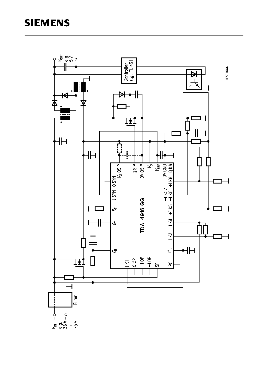
Figure 3
Application Circuit 1: Forward Converter with Output Regulation
TDA 4916 GG
Semiconductor Group
20
05.96
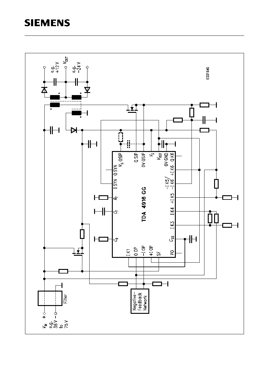
Figure 4
Application Circuit 2: Flyback Converter with EMF Regulation

TDA 4916 GG
Semiconductor Group
21
05.96
Figure 5
Timing Diagram

TDA 4916 GG
Semiconductor Group
22
05.96
Figure 6
Soft Start
C
SS
/ Fault/ON - OFF
TDA 4916 GG
Semiconductor Group
23
05.96
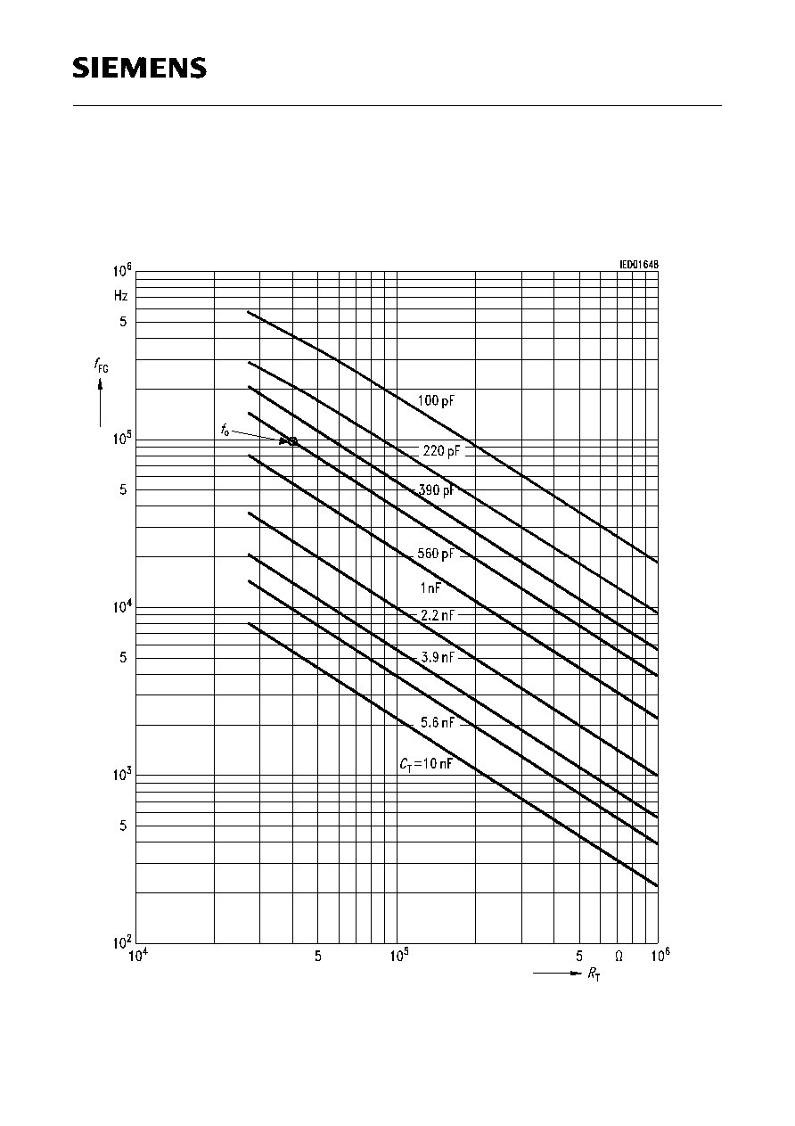
Nomogram for FG
f
o
= 97.5 kHz @
T
j
= 25
∞
C;
R
T
= 40.2 k
;
C
T
= 560 pF
TDA 4916 GG
Semiconductor Group
24
05.96
Instructions for the Approximate Calculation of the Maximum Duty Cycle of the FG
when
R
VS
or
R
GND
is Connected to Input
C
T
.
1. General remarks
Duty cycle
= ON time/period
Time
t
=
C
T
V
CT
/
I
CT
V
CT
= approx. 0.6 V
Current
I
RGND
= 2.2 V/
R
GND
Current
I
RT
= 2.5 V/
R
T
Current
I
RVS
= (12 V
-
2.2 V)/
R
VS
Mean value
V
CT Mean
= approx. 2.2 V
To facilitate better general understanding, the equations are not abbreviated in the
following.
The wanted quantity can be isolated using the rules of arithmetic.
2. Calculation for connection of
R
VS
(
> 0.5)
3. Calculation for connection of
R
GND
(
< 0.5)
max
C
T
0.6 V
I
RT
I
RVS
≠
------------------------------
C
T
0.6 V
I
RT
I
RVS
≠
------------------------------
C
T
0.6 V
I
RT
I
RVS
+
------------------------------
+
--------------------------------------------------------------------
=
max
C
T
0.6 V
I
RT
I
RGND
+
------------------------------------
C
T
0.6 V
I
RT
I
RGND
+
------------------------------------
C
T
0.6 V
I
RT
I
RGND
≠
------------------------------------
+
-------------------------------------------------------------------------------
=
TDA 4916 GG
Semiconductor Group
25
05.96
Duty Cycle Limiting
f
FG
= 100 kHz
Example for
max
= 44 %:
Step
to get 44 % a resistor
R
GND
= 220 k
is found
Step
for the same
we get
R
T
= 39 k
to set
f
FG
to 100 kHz

TDA 4916 GG
Semiconductor Group
26
05.96
Tolerance of Osc. Frequency
f
max
versus Osc. Frequency
f
Tolerance of Duty Cycle
max
versus Osc. Frequency
f

TDA 4916 GG
Semiconductor Group
27
05.96
Package Outlines
P-DSO-24-1 (SMD)
(Plastic Dual Small Outline Package)
GPS05144
Sorts of Packing
Package outlines for tubes, trays etc. are contained in our
Data Book "Package Information"
Dimensions in mm
SMD = Surface Mounted Device