
PA2423L
2.4 GHz Bluetooth Class 1 Power Amplifier IC
Preliminary Information
Applications
Bluetooth
tm
Class 1
USB Dongles
Laptops
Access Points
Cordless Piconets
Features
+22.5dBm at 45% Power Added Efficiency
Low current 80mA typical @ Pout=+20 dBm
Temperature stability better than 1dB
Power-control and Power-down modes
Single 3.3 V Supply Operation
Temperature rating: -40C to +85C
Very small plastic package - 6 lead LPCC
(1.6mm x 3.0mm)
Ordering Information
Type
Package
Shipping
Method
PA2423L
6 - LPCC
Tape and reel
Tubes -samples
PA2423L-EV Evaluation
kit
Product Description
A monolithic, high-efficiency, silicon-germanium
power amplifier IC, the PA2423L is designed for
class 1 Bluetooth
tm
2.4 GHz radio applications. It
delivers +22.5 dBm output power with 45%
power-added efficiency � making it capable of
overcoming insertion losses of up to 2.5 dB
between amplifier output and antenna input in
class 1 Bluetooth
tm
applications.
The amplifier features:
an analog control input for improving PAE at
reduced output power levels;
a digital control input for controlling power up
and power down modes of operation.
An on-chip ramping circuit provides the turn-
on/off switching of amplifier output with less than
3dB overshoot, meeting the Bluetooth
tm
specification 1.1.
The PA2423L operates at 3.3V DC. At typical
output power level (+22.5 dBm), its current
consumption is 125 mA.
The silicon/silicon-germanium structure of the
PA2423L � and its exposed-die-pad package,
soldered to the system PCB � provide high
thermal conductivity and a subsequently low
junction temperature. This device is capable of
operating at a duty cycle of 100 percent.
Functional Block Diagram
Stage 1
Stage 2
Interstage
Match
Bias Generator
Ramp
Circuitry
V
CTL
V
CC0
V
RAMP
IN
OUT/ V
CC2
V
CC1
GND
GND
DOC# 05PDS002 Rev 4
07/26/2001
Page 1 of 11

PA2423L
2.4 GHz Bluetooth Class 1 Power Amplifier IC
Preliminary Information
Pin Out Diagram
TOP VIEW
BOTTOM VIEW
SiGe
2423L
1
2
5
4
3
6
1
2
3
4
5
6
Die
1
2
3
4
5
6
Die
Pin Out Description
Pin No.
Name
Description
1
V
CTL
Controls the output level of the power amplifier. An analog control signal between
0V and Vcc varies the PA output power between minimum and maximum values
2
V
RAMP
Enable/Disable the power amplifier. A digital control signal with Vcc logic high
(power up) and 0V logic low (power down) is used to turn the device on and off.
3 IN
Power amplifier RF input, external input matching network with DC blocking is
required
4
V
CCO
Bias supply voltage
5
V
CC1
Stage 1 collector supply voltage, external inter-stage matching network is required
6
OUT/V
CC2
PA Output and Stage2 collector supply voltage, external output matching network
with DC blocking is required
Die Pad
GND
Heatslug Die Pad is ground
DOC# 05PDS002 Rev 4
07/26/2001
Page 2 of 11

PA2423L
2.4 GHz Bluetooth Class 1 Power Amplifier IC
Preliminary Information
Absolute Maximum Ratings
Symbol
Parameter
Min.
Max.
Unit
V
CC
Supply Voltage
-0.3
+3.6
V
V
CTL
Control Voltage
-0.3
V
CC
V
V
RAMP
Ramping Voltage
-0.3
V
CC
V
IN
RF Input Power
+8
dBm
T
A
Operating Temperature Range
-4
0 +85
�C
T
STG
Storage Temperature Range
-4
0
+150
�C
T
j
Maximum Junction Temperature
+15
0
�C
Operation in excess of any one of above Absolute Maximum Ratings may result in permanent damage. This
device is a high performance RF integrated circuit with ESD rating < 600V and is ESD sensitive. Handling
and assembly of this device should be at ESD protected workstations.
DC Electrical Characteristics
Conditions: V
CC0
= V
CC1
= V
CC2
= V
RAMP
= 3.3V, V
CTL
= 3.3V, P
IN
= +2dBm,T
A
=25
�C, f = 2.45GHz,
Input and Output externally matched to 5
0 ,unless otherwise note
d.
Symbol
Note
Parameter
Min. Typ. Max. Unit
V
CC
Supply Voltage
3 3.3 3.6 V
I
CC
1
Supply Current (I
CC
= I
VCC0
+ I
VCC1
+I
VCC2
), V
CTL
= 3.3V
125
150
mA
Icc
temp
3
Supply Current variation over temperature from T
A
= 25
�C
(-4
0�C <T
A
<+8
5�C)
25 %
V
CTL
PA Output Power Control Voltage Range
0
V
CC
V
I
CTL
1
Current sourced by V
CTL
Pin
200
250
�A
3
Logic High Voltage
2.0 V
V
RAMP
3
Logic Low Voltage
0.8
V
I
stdby
1
Leakage Current when V
ramp
= 0V, V
ctl
= high
0.5 10
�A
DOC# 05PDS002 Rev 4
07/26/2001
Page 3 of 11

PA2423L
2.4 GHz Bluetooth Class 1 Power Amplifier IC
Preliminary Information
AC Electrical Characteristics
Conditions: V
CC0
= V
CC1
= V
CC2
= V
RAMP
=3.3V, V
CTL
= 3.3V, PIN =+2 dBm, T
A
=25
�C, f =2.45 GHz,
Input and Output externally matched to 5
0, unless otherwise noted.
Symbol
Note
Parameter
Min. Typ.
Max. Unit
f
L-U
3
Frequency Range
2400 2500
MHz
1
Output Power @ P
IN
=+2 dBm, V
CTL
= 3.3V
20 22.5 23.5 dBm
P
out
1
Output Power @ P
IN
=+2 dBm, V
CTL
=0.4V
-20 0 dBm
P
temp
3
Output Power variation over temperature (-4
0�C <T
A
<+8
5�C)
1 2 dB
dP
OUT
/dVCTL
3
Control Voltage Sensitivity
120
dBm/V
PAE
Power Added Efficiency at +22.5 dBm Output Power
45 %
G
VAR
3
Gain Variation over band (2400-2500 MHz)
0.7
1.0 dB
2f, 3f, 4f, 5f
3.4
Harmonics
-40
-35
dBc
IS21 IOFF
2
Isolation in "OFF" State, P
IN
= +2dBm, V
RAMP
= 0V
15 20 dB
IS12I
2
Reverse Isolation
32 42 dB
STAB
2
Stability (P
IN
= +2dBm, Load VSWR = 6:1)
All non-harmonically related
outputs less than -50 dBc
Notes: (1) Guaranteed by production test at T
A
=25
�C.
(2) Guaranteed by design only
(3) Guaranteed by design and characterization
(4) Harmonic levels are greatly affected by topology of external matching networks.
Typical Performance Characteristics
Test Conditions: SiGe PA2423L-EV: V
CC0
=V
CC1
=V
CC2
=V
RAMP
=3.3V, V
CTL
= 3.3V, P
IN
= +2 dBm, T
A
= 25
�C, f
= 2.45GHz, Input and Output externally matched to 50
, unless otherwise noted.
Pout, Icc vs Supply Voltage
14
15
16
17
18
19
20
21
22
23
24
2.4
2.6
2.8
3
3.2
3.4
3.6
Vcc(V)
Output Power
(dBm)
70
78
86
94
102
110
118
126
134
142
150
Supply current
(mA)
Pout
Icc
Output Power, Gain vs Input Power
0
5
10
15
20
25
-28
-24
-20
-16
-12
-8
-4
0
4
8
Input Power (dBm)
Output Powe
r (dBm)
5.00
10.00
15.00
20.00
25.00
30.00
Gain (dB)
Pout
Gain
DOC# 05PDS002 Rev 4
07/26/2001
Page 4 of 11

PA2423L
2.4 GHz Bluetooth Class 1 Power Amplifier IC
Preliminary Information
PAE vs Input Power
0
5
10
15
20
25
30
35
40
45
50
-28
-24
-20
-16
-12
-8
-4
0
4
8
Input Power(dBm)
PAE (%
)
Pout vs Frequency
18. 0
18. 5
19. 0
19. 5
20. 0
20. 5
21. 0
21. 5
22. 0
22. 5
23. 0
2. 2
2. 3
2. 4
2. 5
2. 6
2. 7
Frequency (GHz)
Output Power (dBm)
DOC# 05PDS002 Rev 4
07/26/2001
Page 5 of 11

PA2423L
2.4 GHz Bluetooth Class 1 Power Amplifier IC
Preliminary Information
Supply Current vs. Control
Voltage
0
20
40
60
80
100
120
140
0.4
0.9
1.4
1.9
2.4
2.9
3.4
Vctl(V)
Supply Current
(mA)
Pin=-4dBm
Pin=0dBm
Pin=+2dBm
Output Power vs Control Voltage
-25
-20
-15
-10
-5
0
5
10
15
20
25
0.4
0.9
1.4
1.9
2.4
2.9
3.4
Vctl(V)
Output Power dBm)
Pin=-4dBm
Pin=0dBm
Pin=+2dBm
Icc vs Frequency
60
70
80
90
100
110
120
130
140
2.3
2.3
2.4
2.4
2.5
2.5
2.6
2.6
2.7
Frequency (GHz)
Supply Current (mA)
Harmonic Output Spectrum
-50
-45
-40
-35
-30
-25
-20
-15
-10
-5
0
5
10
15
20
25
30
1
2
3
4
5
6
7
8
9
10
11 12
13
Frequency (GHz)
RFout power (dBm)
DOC# 05PDS002 Rev 4
07/26/2001
Page 6 of 11

PA2423L
2.4 GHz Bluetooth Class 1 Power Amplifier IC
Preliminary Information
PA output spectrum with BT modulated signal
-60
-50
-40
-30
-20
-10
0
10
20
30
2.4475
2.4485
2.4495
2.4505
2.4515
2.4525
Frequency (GHz)
RF
Ou
tp
u
t
P
o
we
r (d
Bm) in
to
5
0
R
DOC# 05PDS002 Rev 4
07/26/2001
Page 7 of 11
PA2423L
2.4 GHz Bluetooth Class 1 Power Amplifier IC
Preliminary Information
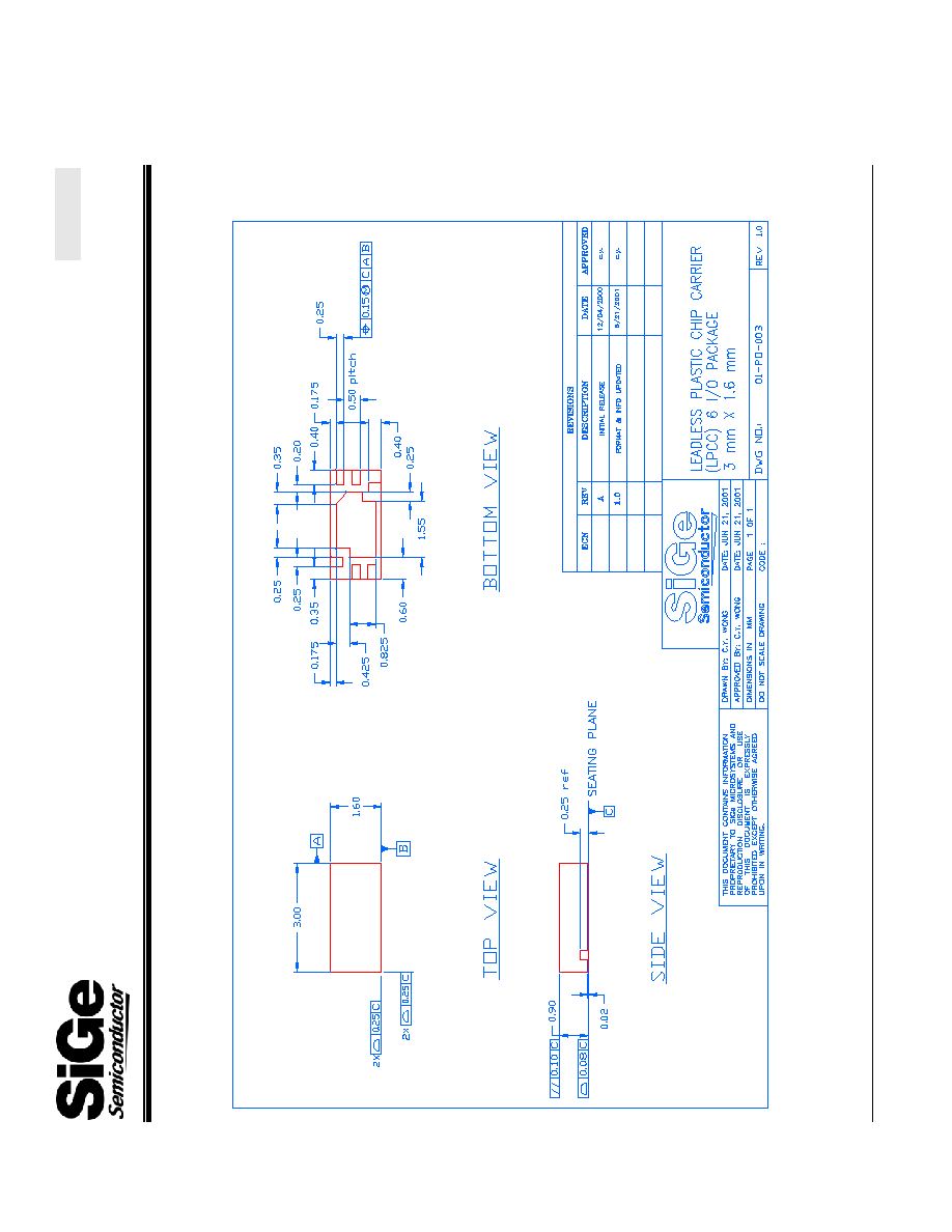
Package Dimensions
The PA2423L is packaged in a 1.6 mm x 3.0 mm 6 lead LPCC package. The underside of the package is an exposed die-pad structure. This allows for
direct soldering to the PCB for enhanced thermal conductivity. The package dimensions are shown in the drawing below.
DOC# 05PDS002 Rev 4
07/26/2001
Page 8 of 11

PA2423L
2.4 GHz Bluetooth Class 1 Power Amplifier IC
Preliminary Information
LPCC 6 PCB Footprint Layout
Applications Information
For test and design purposes, SiGe Semiconductor offers an evaluation board for the PA2423L. The order
part number for the evaluation board is PA2423L-EV. The evaluation board is intended to simplify the
testing with respect to RF performance of this power amplifier.
The application note, 05AN006 provides the supporting information for using the evaluation board. It
contains information on the schematic, bill of materials and recommended layout for the power amplifier and
the input and output matching networks. To assist in the design process, this layout is available, upon
request, in gerber file format.
Using V
RAMP
V
RAMP
is a digital pin used to power-up and power-down the PA2423L in Time Duplex systems such as
Bluetooth
tm
1.1. During receive mode, V
RAMP
voltage is pulled down, PA2423L acts as a 25 dB isolation block
between the radio and the antenna while consuming a modest 1uA. In transmit mode, V
RAMP
voltage is
pulled to VCC and PA2423L offers 19 dB to 21dB of large signal gain. The rise and fall time are in the order
of 1-2usec.
DOC# 05PDS002 Rev 4
07/26/2001
Page 9 of 11

PA2423L
2.4 GHz Bluetooth Class 1 Power Amplifier IC
Preliminary Information
Using V
CTL
V
CTL
is an analog pin that is designed to control the gain of PA2423L. Applying a voltage between 0V and
Vcc will adjust the gain between -15dB and 21 dB. Used in combination with a variable drive level to
PA2423L, the V
CTL
function can greatly optimize the PAE of the system at all four Bluetooth
tm
transmitted
power levels.
By applying approximately 1.4V to V
CTL
, for example, a Class1 radio can be modified to a Class2 radio with
the PA2423L consuming only 15mA.
By implementing a resistor DAC, the V
CTL
pin can interface with Bluetooth
tm
transceivers offering digital and
programmable outputs.
DOC# 05PDS002 Rev 4
07/26/2001
Page 10 of 11

PA2423L
2.4 GHz Bluetooth Class 1 Power Amplifier IC
Preliminary Information
http://www.sige.com
Headquarters: Canada
Phone: +1 613 820 9244
Fax: +1 613 820 4933
2680 Queensview Drive
Ottawa ON K2B 8J9 Canada
sales@sige.com
U.S.A.
United
Kingdom
19925 Stevens Creek Blvd.
1010 Cambourne Business Park
Suite 135
Cambourne
Cupertino, CA 95014-2358
Cambridge CB3 6DP
Phone: +1 408 973 7835
Phone: +44 1223 598 444
Fax:
+1 408 973 7235
Fax:
+44 1223 598 035
Information furnished is believed to be accurate and reliable and is provided on an "as is" basis. SiGe Semiconductor Inc.
assumes no responsibility or liability for the direct or indirect consequences of use of such information nor for any
infringement of patents or other rights of third parties, which may result from its use. No license or indemnity is granted by
implication or otherwise under any patent or other intellectual property rights of SiGe Semiconductor Inc. or third parties.
Specifications mentioned in this publication are subject to change without notice. This publication supersedes and
replaces all information previously supplied. SiGe Semiconductor Inc. products are NOT authorized for use in
implantation or life support applications or systems without express written approval from SiGe Semiconductor Inc.
The Bluetooth trademarks are owned by Bluetooth SIG Inc., USA.
Copyright 2001 SiGe Semiconductor
All Rights Reserved
DOC# 05PDS002 Rev 4
07/26/2001
Page 11 of 11