 | ÐлекÑÑоннÑй компоненÑ: S-818A50A | СкаÑаÑÑ:  PDF PDF  ZIP ZIP |
S818_E1.3_10

Rev.1.3
_10
LOW DROPOUT CMOS VOLTAGE REGULATOR
S-818 Series
Seiko Instruments Inc.
1
The S-818 Series is a positive voltage regulator
developed by CMOS technology and featured by low
dropout voltage, high output voltage accuracy and low
current consumption.
Built-in low on-resistance transistor provides low
dropout voltage and large output current. A ceramic
capacitor of 2
µF or more can be used as an output
capacitor. A shutdown circuit ensures long battery life.
The SOT-23-5 miniaturized package and the SOT-89-5
package are recommended for configuring portable
devices and large output current applications,
respectively.
Features
· Low current consumption:
At operation mode: Typ. 30
µA, Max. 40 µA
At shutdown mode: Typ. 100 nA, Max. 500 nA
· Output voltage:
2.0 to 6.0 V, selectable in 0.1 V steps.
· High accuracy output voltage: ±2.0%
· Peak output current:
200 mA capable (3.0 V output product, V
IN
=4 V)
*1
300 mA capable (5.0 V output product, V
IN
=6 V)
*1
· Low dropout voltage:
Typ. 170 mV (5.0 V output product, I
OUT
=60 mA)
· A ceramic capacitor (2 µF or more) can be used as an output capacitor.
· Built-in shutdown circuit
· Small package:
SOT-23-5, SOT-89-5
*1. Attention should be paid to the power dissipation of the package when the output current is large.
Applications
· Power source for battery-powered devices, personal communication devices and home electric/electronic
appliances
Packages
· SOT-23-5 (Package drawing code: MP005-A)
· SOT-89-5 (Package drawing code: UP005-A)
LOW DROPOUT CMOS VOLTAGE REGULATOR
S-818 Series
Rev.1.3
_10
2
Seiko Instruments Inc.
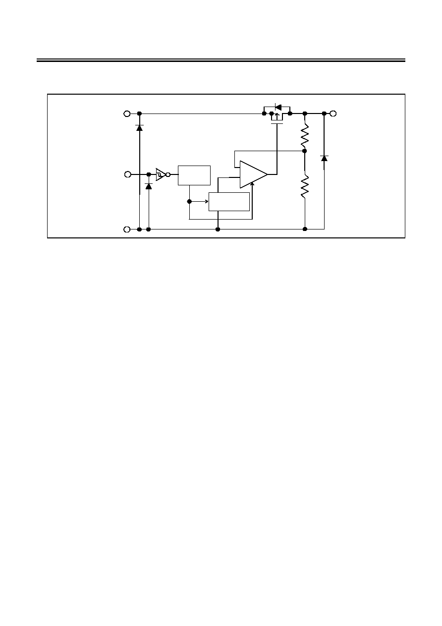
Block Diagram
VOUT
ON/OFF
VSS
VIN
*1
ON/OFF
circuit
Reference
voltage
+
-
*1. Parasitic diode
Figure 1
LOW DROPOUT CMOS VOLTAGE REGULATOR
Rev.1.3
_10
S-818 Series
Seiko Instruments Inc.
3
Product Code Structure
1. Product name selection guide
S-818 x xx A xx - xxx -
T2
IC direction in tape specifications
*1
Product name (abbreviation)
*2
Package name (abbreviation)
MC: SOT-23-5
UC: SOT-89-5
Output voltage
20 to 60
(E.g., When the output voltage is 2.0 V, it is
expressed as 20.)
Product type
*3
A: ON/OFF pin positive logic, high active
B: ON/OFF pin negative logic, low active
*1. Refer to the taping specifications at the end of this book.
*2. Refer to the "Table 1" under the "2. Product name list".
*3. Refer to "3. ON/OFF pin (Shutdown pin)" under the " Operation".
2. Product name list
Table 1
Package
Output Voltage
SOT-23-5 SOT-89-5
2.0 V±2.0 %
S-818A20AMC-BGA-T2
S-818A20AUC-BGA-T2
2.5 V±2.0 %
S-818A25AMC-BGF-T2
S-818A25AUC-BGF-T2
2.8 V±2.0 %
S-818A28AMC-BGI-T2
S-818A28AUC-BGI-T2
3.0 V±2.0 %
S-818A30AMC-BGK-T2
S-818A30AUC-BGK-T2
3.1 V±2.0 %
S-818A31AMC-BGL-T2
3.2 V±2.0 %
S-818A32AMC-BGM-T2
S-818A32AUC-BGM-T2
3.3 V±2.0 %
S-818A33AMC-BGN-T2
S-818A33AUC-BGN-T2
3.5 V±2.0 %
S-818A35AUC-BGP-T2
3.6 V±2.0 %
S-818A36AMC-BGQ-T2
S-818A36AUC-BGQ-T2
3.8 V±2.0 %
S-818A38AMC-BGS-T2
S-818A38AUC-BGS-T2
4.0 V±2.0 %
S-818A40AMC-BGU-T2
S-818A40AUC-BGU-T2
5.0 V±2.0 %
S-818A50AMC-BHE-T2
S-818A50AUC-BHE-T2
6.0 V
±2.0 %
S-818A60AUC-BHO-T2
Remark Please contact the SII marketing department for products with an output voltage over than
those specified above.
LOW DROPOUT CMOS VOLTAGE REGULATOR
S-818 Series
Rev.1.3
_10
4
Seiko Instruments Inc.
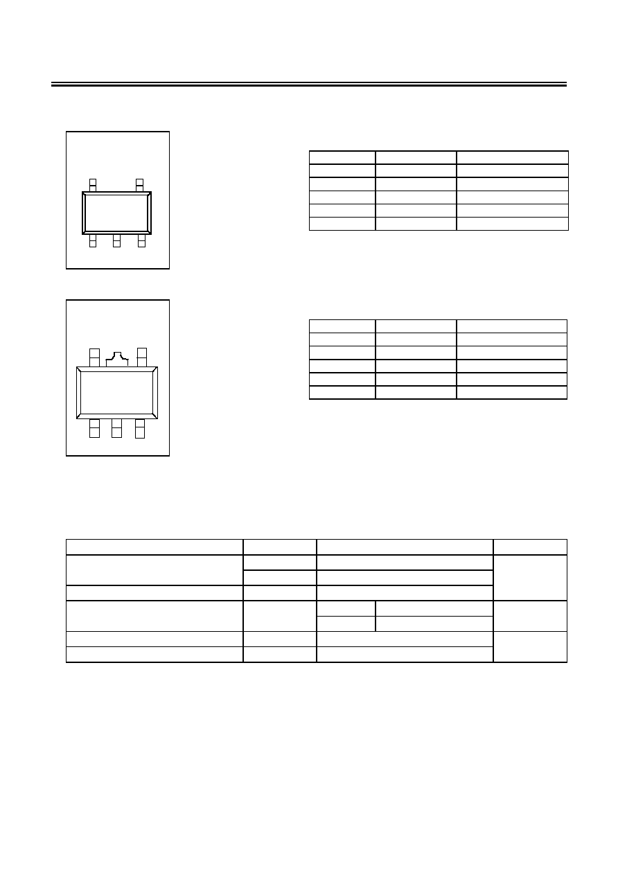
Pin Configurations
Table 2
Pin No.
Symbol
Pin description
1
VIN
Input
voltage
pin
2
VSS
GND
pin
3
ON/OFF
Shutdown pin
4
NC
*1
No connection
5
VOUT
Output voltage pin
SOT-23-5
Top view
5
4
3
2
1
*1. The NC pin is electrically open.
The NC pin can be connected to VIN or VSS.
Figure 2
Table 3
Pin No.
Symbol
Pin description
1
VOUT
Output voltage pin
2 VSS
GND
pin
3
NC
*1
No connection
4
ON/OFF Shutdown
pin
5
VIN Input
voltage
pin
SOT-89-5
Top view
1
3
2
4
5
*1. The NC pin is electrically open.
The NC pin can be connected to VIN or VSS.
Figure 3
Absolute Maximum Ratings
Table 4
(Ta
=25°C unless otherwise specified)
Item
Symbol
Absolute Maximum Rating
Unit
Input voltage
V
IN
V
SS
-0.3 to V
SS
+12 V
V
ON/OFF
V
SS
-0.3 to V
SS
+12
Output voltage
V
OUT
V
SS
-0.3 to V
IN
+0.3
Power dissipation
P
D
SOT-23-5
250
mW
SOT-89-5
500
Operating ambient temperature
Topr
-40 to +85
°C
Storage ambient temperature
Tstg
-40 to +125
Caution The absolute maximum ratings are rated values exceeding which the product could suffer
physical damage. These values must therefore not be exceeded under any conditions.
LOW DROPOUT CMOS VOLTAGE REGULATOR
Rev.1.3
_10
S-818 Series
Seiko Instruments Inc.
5
Electrical Characteristics
Table 5
(Ta
=25°C unless otherwise specified)
Parameter Symbol
Conditions
Min.
Typ.
Max.
Unit
Test
circuit
Output voltage
*1
V
OUT(E)
V
IN
=V
OUT(S)
+1 V, I
OUT
=30 mA
V
OUT(S)
×0.98
V
OUT(S)
V
OUT(S)
×1.02
V 1
Output current
*2
I
OUT
2.0 V
V
OUT(S)
2.4 V 100
*5
mA 3
V
OUT(S)
+1 V
V
IN
10 V
2.5 V
V
OUT(S)
2.9 V 150
*5
3.0 V
V
OUT(S)
3.9 V 200
*5
4.0 V
V
OUT(S)
4.9 V 250
*5
5.0 V
V
OUT(S)
6.0 V 300
*5
Dropout voltage
*3
V
drop
I
OUT
=60 mA 2.0 VV
OUT(S)
2.4 V
0.51 0.87 V 1
2.5 V
V
OUT(S)
2.9 V
0.38 0.61
3.0 V
V
OUT(S)
3.4 V
0.30 0.44
3.5 V
V
OUT(S)
3.9 V
0.24 0.33
4.0 V
V
OUT(S)
4.4 V
0.20 0.26
4.5 V
V
OUT(S)
4.9 V
0.18 0.22
5.0 V
V
OUT(S)
5.4 V
0.17 0.21
5.5 V
V
OUT(S)
6.0 V
0.17 0.20
Line regulation 1
OUT
IN
1
OUT
V
V
V
·
V
OUT(S)
+0.5 VV
IN
10 V,
I
OUT
=30 mA
0.05 0.2
%/V
Line regulation 2
OUT
IN
2
OUT
V
V
V
·
V
OUT(S)
+0.5 VV
IN
10 V,
I
OUT
=10 µA
0.05 0.2
Load regulation
V
OUT3
V
IN
=V
OUT(S)
+1 V,
10
µAI
OUT
80 mA
30 50
mV
Output voltage
temperature coefficient
*4
OUT
OUT
V
Ta
V
·
V
IN
=V
OUT(S)
+1 V, I
OUT
=30 mA,
-40°CTa85°C
±100
ppm
/
°C
Current consumption
at operation
I
SS1
V
IN
=V
OUT(S)
+1 V,
ON/OFF pin
=ON, no load
30 40
µA
2
Current consumption
at shutdown
I
SS2
V
IN
=V
OUT(S)
+1 V,
ON/OFF pin
=OFF, no load
0.1 0.5
Input voltage
V
IN
10 V 1
Shutdown pin
input voltage "H"
V
SH
V
IN
=V
OUT(S)
+1 V, R
L
=1 k,
Judged by V
OUT
output level.
1.5
4
Shutdown pin
input voltage "L"
V
SL
V
IN
=V
OUT(S)
+1 V, R
L
=1 k,
Judged by V
OUT
output level.
0.3
Shutdown pin
input current "H"
I
SH
V
IN
=V
OUT(S)
+1 V, V
ON/OFF
=7 V
-0.1
0.1
µA
Shutdown pin
input current "L"
I
SL
V
IN
=V
OUT(S)
+1 V, V
ON/OFF
=0 V
-0.1
0.1
Ripple rejection
RR
V
IN
=V
OUT(S)
+1 V, f=100 Hz,
V
rip
=0.5 V p-p, I
OUT
=30 mA
45
dB 5
Document Outline
- S-818 Series
- Cover
- Features
- Applications
- Packages
- Block Diagram
- Product Code Structure
- Pin Configurations
- Absolute Maximum Ratings
- Electrical Characteristics
- Test Circuits
- Application Conditions
- Standard Circuit
- Technical Terms
- Description of Operation
- Selection of Output Capacitor (CL)
- Precautions
- Characteristics (Typical data)
- Transient Response Characteristics (S-818A30A, Typical data, Ta=25°C)
- Package Drawings