 | –≠–ª–µ–∫—Ç—Ä–æ–Ω–Ω—ã–π –∫–æ–º–ø–æ–Ω–µ–Ω—Ç: SII161A | –°–∫–∞—á–∞—Ç—å:  PDF PDF  ZIP ZIP |

Silicon Image, Inc.
Subject to Change without Notice
Si
I
161A PanelLink
Æ
Receiver
Datasheet
March 2000
General Description
Features
The Si
I
161A receiver uses PanelLink Digital technology to support high
resolution displays up to UXGA. The Si
I
161A receiver supports up to true
color panels (24 bit/pixel, 16.7M colors) in 1 or 2 pixels/clock mode. In
addition, the receiver data output is time staggered to reduce ground bounce
that affects EMI. Since all PanelLink products are designed on scaleable
CMOS architecture to support future performance requirements while
maintaining the same logical interface, system designers can be assured that
the interface will be fixed through a number of technology and performance
generations.
PanelLink Digital technology simplifies PC and display interface design
by resolving many of the system level issues associated with high-speed
mixed signal design, providing the system designer with a digital interface
solution that is quicker to market and lower in cost.
∑
Low Power: 3.3V core operation
∑
Time staggered data output for reduced ground
bounce
∑
Sync Detect: for Plug & Display "Hot Plugging"
∑
Cable Distance Support: over 5m with twisted-pair,
fiber-optics ready
∑
Compliant with DVI 1.0 (DVI is backwards
compatible with VESA
Æ
P&D
TM
and DFP)
Si
I
161
A Pin Diagram
RSVD
1
SiI 161A
100-Pin TQFP
(Top View)
PD
2
ST
3
PIXS
4
GND
5
VCC
6
STAG_OUT
7
SCDT
8
PDO
9
QE0
10
QE1
11
QE2
12
QE3
13
QE4
14
QE5
15
QE6
16
QE7
17
OVCC
18
OGND
19
QE8
20
QE9
21
QE10
22
QE11
23
QE12
24
QE13
25
QE14
26
QE15
27
OGND
28
OVCC
29
QE16
30
QE17
31
QE18
32
QE19
33
QE20
34
QE21
35
QE22
36
QE23
37
VCC
38
GND
39
CTL1
40
CTL2
41
CTL3
42
OVCC
43
ODCK
44
OGND
45
DE
46
VSYNC
47
HSYNC
48
QO0
49
QO1
50
75
QO21
74
QO20
73
QO19
72
QO18
71
QO17
70
QO16
69
GND
68
VCC
67
QO15
66
QO14
65
QO13
64
QO12
63
QO11
62
QO10
61
QO9
60
QO8
59
OGND
58
OVCC
57
QO7
56
QO6
55
QO5
54
QO4
53
QO3
52
QO2
51
QO22
OCK_INV
1
0
0
RESERVED
99
PGND
98
PVCC
97
EXT_RES
96
AVCC
95
RXC-
94
RXC+
9
3
AGND
92
RX0-
9
1
RX0+
90
AGND
89
AVCC
88
AGND
87
RX1-
8
6
RX1+
85
AVCC
8
4
AGND
83
AVCC
82
RX2-
81
RX2+
80
AGND
79
OVCC
78
QO23
77
OGND
76
DIFFERENTIAL
SIGNAL
ODD 8-bits RED
EVEN 8-bits RED
ODD 8-bits GREEN
EVEN 8-bits GREEN
ODD 8-bits BLUE
EVEN 8-bits BLUE
CONFIG. PINS
PLL
PWR
MANAGEMENT
GPO
OUTPUT CLOCK
CONTROLS
Silicon Image, Inc.
SiI 161
A
SiI
/DS-0009-A
Silicon Image, Inc.
2
Subject to Change without Notice
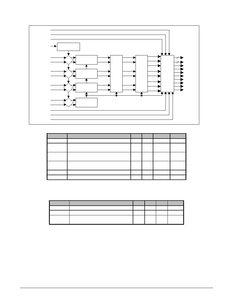
Functional Block Diagram
Absolute Maximum Conditions
Symbol
Parameter
Min
Typ
Max
Units
V
CC
Supply Voltage 3.3V
-0.3
4.0
V
V
I
Input Voltage
-0.3
V
CC
+
0.3
V
V
O
Output Voltage
-0.3
V
CC
+
0.3
V
T
A
Ambient Temperature (with power
applied)
-25
105
∞
C
T
STG
Storage Temperature
-40
125
∞
C
P
PD
Package Power Dissipation
1.8
W
Notes:
1
Permanent device damage may occur if absolute maximum conditions are exceeded.
2
Functional operation should be restricted to the conditions described under Normal Operating Conditions.
Normal Operating Conditions
Symbol
Parameter
Min
Typ
Max
Units
V
CC
Supply Voltage
3.00
3.3
3.6
V
V
CCN
Supply Voltage Noise
100
mV
P-P
T
A
Ambient Temperature (with power
applied)
0
25
70
∞
C
CTL3
RX2+
RX2-
RX1+
RX1-
RX0+
RX0-
RXC+
RXC-
SYNC2
EXT_RES
PDO
ST
ODCK
PIXS
DF0
OCK_INV
STAG_OUT
Data Recovery
CH2
VCR
Termination
Control
Data Recovery
CH1
VCR
Data Recovery
CH0
VCR
PLL
VCR
SYNC1
SYNC0
Channel
SYNC
SYNC2
SYNC1
SYNC0
Decoder
CTL2
CTL1
VSYNC
HSYNC
Panel
Inter-
face
Logic
QE[23:0]
24
QO[23:0]
24
DE
HSYNC
VSYNC
CTL3
CTL2
CTL1
SCDT
DATA
DATA
DATA
Silicon Image, Inc.
SiI 161
A
SiI
/DS-0009-A
Silicon Image, Inc.
3
Subject to Change without Notice
DC Digital I/O Specifications
Under normal operating conditions unless otherwise specified.
Symbol
Parameter
Conditions
Min
Typ
Max
Units
V
IH
High-level Input
Voltage
2
V
V
IL
Low-level Input
Voltage
0.8
V
V
OH
High-level Output
Voltage
2.4
V
V
OL
Low-level Output
Voltage
0.4
V
V
CINL
Input Clamp Voltage
1
I
CL
= -18mA
GND -0.8
V
V
CIPL
Input Clamp Voltage
1
I
CL
= 18mA
IVCC + 0.8
V
V
CONL
Output Clamp
Voltage
1
I
CL
= -18mA
GND -0.8
V
V
COPL
Output Clamp
Voltage
1
I
CL
= 18mA
OVCC + 0.8
V
I
OL
Output Leakage
Current
High
Impedance
-10
10
µ
A
Note:
1
Guaranteed by design.
DC Specifications
Under normal operating conditions unless otherwise specified.
Symbol
Parameter
Conditions
Min
Typ
Max
Units
I
OHD
Output High Drive Data and
Controls
V
OUT
= V
OH
; ST = 1
ST = 0
4.2
2.1
8
4
18
9
mA
I
OLD
Output Low Drive Data and
Controls
V
OUT
= V
OL
; ST = 1
ST = 0
-5.2
-2.6
-5.5
-2.75
-11
-5.5
mA
I
OHC
ODCK High Drive
V
OUT
= V
OH
; ST = 1
ST = 0
8.5
4.2
17
9
37
18
mA
I
OLC
ODCK Low Drive
V
OUT
= V
OL
; ST = 1
ST = 0
-10.4
-5.2
-16
-8
-23
-11
mA
V
ID
Differential Input Voltage
Single Ended Amplitude
75
1000
mV
I
PD
Power-down Current
2
10
mA
I
CCR
Receiver Supply Current
DCLK=82.5MHz,
2-pixel/clock mode
C
LOAD
= 10pF
R
EXT_SWING
= 560
Typical Pattern
3
240
270
mA
DCLK=82.5MHz,
2-pixel/clock mode
C
LOAD
= 10pF
R
EXT_SWING
= 560
Worse Case Pattern
4
270
330
mA
Notes:
1
Guaranteed by design.
2
The transmitter must be in power-down mode, powered off, or disconnected for the current to be under this maximum.
3
The Typical Pattern contains a gray scale area, checkerboard area, and text.
4
Black and white checkerboard pattern, each checker is two pixel wide.
Silicon Image, Inc.
SiI 161
A
SiI
/DS-0009-A
Silicon Image, Inc.
4
Subject to Change without Notice
AC Specifications
Under normal operating conditions unless otherwise specified.
Symbol
Parameter
Conditions
Min
Typ
Max
Units
T
DPS
Intra-Pair (+ to -) Differential Input Skew
1
165MHz
1 pixel/clock
245
ps
T
CCS
Channel to Channel Differential Input Skew
1
165MHz
1 pixel/clock
4
ns
T
IJIT
Worst Case Differential Input Clock Jitter
tolerance
2,3
65 MHz
1 pixel/clock
465
ps
112 MHz
1 pixel/clock
270
ps
165 MHz
1 pixel/clock
182
ps
D
LHT
Low-to-High Transition Time
Data and Controls
C
L
= 10pF;
ST = 1
2.2
ns
(measured at 70 C, 82.5 MHz, 2-pixel/clock,
PIXS=1)
C
L
= 5pF;
ST = 0
2.5
ns
ODCK
C
L
= 10pF;
ST = 1
2.0
ns
(measured at 70 C, 82.5 MHz, 2-pixel/clock,
PIXS=1)
C
L
= 5pF;
ST = 0
1.5
ns
D
HLT
High-to-Low Transition Time
Data and Controls
C
L
= 10pF;
ST = 1
2.2
ns
(measured at 70 C, 82.5 MHz, 2-pixel/clock,
PIXS=1)
C
L
= 5pF;
ST = 0
2.2
ns
ODCK
C
L
= 10pF;
ST = 1
1.5
ns
(measured at 70 C, 82.5 MHz, 2-pixel/clock,
PIXS=1)
C
L
= 5pF;
ST = 0
1.0
ns
T
SOF
Data, DE, VSYNC, HSYNC, and CTL[3:1] Setup
Time to ODCK falling edge
(OCK_INV = 0, 165MHz, 1-pixel/clock, PIXS = 0)
C
L
= 10pF;
ST = 1
0.5
ns
C
L
= 5pF;
ST = 0
0.5
ns
(OCK_INV = 1, 165MHz, 1-pixel/clock, PIXS = 0)
C
L
= 10pF;
ST = 1
3.0
ns
C
L
= 5pF;
ST = 0
2.0
ns
T
HOF
Data, DE, VSYNC, HSYNC, and CTL[3:1] Hold Time
to ODCK falling edge
(OCK_INV = 0, 165MHz, 1-pixel/clock, PIXS = 0)
C
L
= 10pF;
ST = 1
3.0
ns
C
L
= 5pF;
ST = 0
3.0
ns
(OCK_INV = 1, 165MHz, 1-pixel/clock, PIXS = 0)
C
L
= 10pF;
ST = 1
1.2
ns
C
L
= 5pF;
ST = 0
1.2
ns
Notes:
1
Guaranteed by design.
2
Jitter defined as per DVI 1.0 Specification, Section 4.6 Jitter Specification.
3
Jitter measured with Clock Recovery Unit as per DVI 1.0 Specification, Section 4.7 Electrical Measurement Procedures.
4
Output clock duty cycle is independent of the differential input clock duty cycle and the IDCK duty cycle.
5
Measured when transmitter was powered down (see Si
I
/AN-0005 "PanelLink Basic Design/Application Guide," Section 2.4).
Silicon Image, Inc.
SiI 161
A
SiI
/DS-0009-A
Silicon Image, Inc.
5
Subject to Change without Notice
AC Specifications (continued)
Under normal operating conditions unless otherwise specified.
Symbol
Parameter
Conditions
Min
Typ
Max
Units
R
CIP
ODCK Cycle Time
1
(1-pixel/clock)
6.06
40
ns
F
CIP
ODCK Frequency
1
(1-pixel/clock)
25
165
MHz
R
CIP
ODCK Cycle Time
1
(2-pixels/clock)
12.1
80
ns
F
CIP
ODCK Frequency
1
(2-pixels/clock)
12.5
82.5
MHz
R
CIH
ODCK High Time
4
(165MHz, 1-pixel/clock, PIXS = 0)
C
L
= 10pF;
ST = 1
1.1
ns
C
L
= 5pF;
ST = 0
1.5
ns
R
CIL
ODCK Low Time
4
(165MHz, 1-pixel/clock, PIXS = 0)
C
L
= 10pF;
ST = 1
2.0
ns
C
L
= 5pF;
ST = 0
2.3
ns
T
PDL
Delay from PD Low to high impedance outputs
1
10
ns
T
HSC
Link disabled (DE inactive) to SCDT low
1
100
ms
Link disabled (Tx power down) to SCDT low
5
250
ms
T
FSC
Link enabled (DE active) to SCDT high
1
25
DE
edges
T
ST
ODCK high to even data output
1
0.25
R
CIP
Notes:
1
Guaranteed by design.
2
Jitter defined as per DVI 1.0 Specification, Section 4.6 Jitter Specification.
3
Jitter measured with Clock Recovery Unit as per DVI 1.0 Specification, Section 4.7 Electrical Measurement Procedures.
4
Output clock duty cycle is independent of the differential input clock duty cycle and the IDCK duty cycle.
5
Measured when transmitter was powered down (see Si
I
/AN-0005 "PanelLink Basic Design/Application Guide," Section 2.4).