Preliminary Rev. 0.2 8/05
Copyright © 2005 by Silicon Laboratories
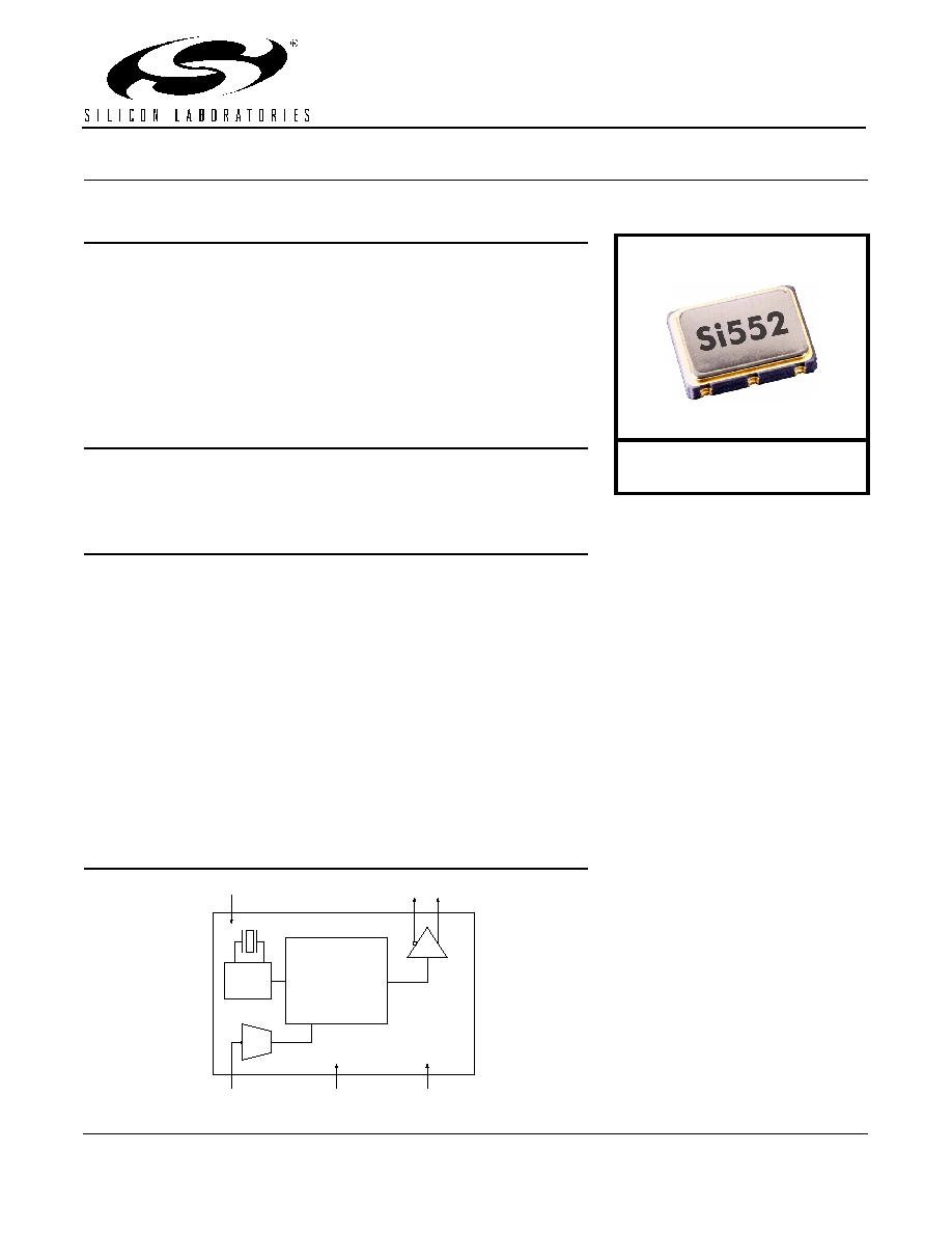
Si552
This information applies to a product under development. Its characteristics and specifications are subject to change without notice.
Si552
D
U A L
F
R E Q U E N C Y
VCXO (10 MH
Z
T O
1.4 GH
Z
)
Features
Applications
Description
The Si552 dual frequency VCXO utilizes Silicon Laboratories advanced
DSPLL
Æ
circuitry to provide a very low jitter clock for all output frequencies.
The Si552 is available with any-rate output frequency from 10 to 945 MHz
and selected frequencies to 1400 MHz. Unlike traditional VCXO's where a
different crystal is required for each output frequency, the Si552 uses one
fixed crystal frequency to provide a wide range of output frequencies. This
IC based approach allows the crystal resonator to be optimized for superior
frequency stability and reliability. In addition, DSPLL clock synthesis
provides superior supply noise rejection, simplifying the task of generating
low jitter clocks in noisy environments often found in communication
systems. The Si552 IC based VCXO is factory configurable for a wide
variety of user specifications including frequency, supply voltage and output
format. Specific configurations are factory programmed into the Si552 at
time of shipment, thereby eliminating the long lead times associated with
custom oscillators.
Functional Block Diagram
Available with any-rate output
frequencies from 10 to 945 MHz and
selected frequencies to 1.4 GHz
Two selectable output frequencies
Industry-standard 7x5 mm package
Available CMOS, LVPECL, LVDS &
CML outputs
3x better frequency stability than
SAW-based oscillators
3rd generation DSPLL
Æ
with
superior jitter performance
Internal fixed crystal frequency
ensures high reliability and low
aging
Lead-free/RoHS-compliant
SONET / SDH
xDSL
10 GbE LAN / WAN
Low jitter clock generation
Optical Modules
Test and Measurement
Fixed
Frequency XO
Any-rate
10≠1400 MHz
DSPLLTM
Clock Synthesis
V
DD
CLK+
CLK-
V
C
GND
FS
ADC
Ordering Information:
See page 7.
Si5602
P
R E L I M I N A R Y
D
A TA
S
H E E T

Si552
2
Preliminary Rev. 0.2
1. Electrical Specifications
Table 1. Si552 Electrical Specifications
Parameter
Min
Typ
Max
Units
Notes
Frequency
Nominal Frequency
LVDS/CML/LVPECL
CMOS
10
10
--
--
945
160
MHz
Specified at time of order by P/N.
Also available in bands from
970 to 1134 MHz and 1213 to
1417 MHz.
Initial Accuracy
≠1.5
--
1.5
ppm
Measured at +25 ∞C at time of ship-
ping and at V
C
= V
DD
/2.
Temperature Stability
≠20
≠50
≠100
--
--
--
+20
+50
+100
ppm
Selectable option by P/N. See
Section 4. "Ordering Information" on
page 7. Measured at V
C
= V
DD
/2.
Linearity
BSL
Incremental
≠5
≠10
±1
±5
+5
+10
%
BSL determined from deviation from
best straight line fit with V
C
ranging
from 10 to 90% of V
DD
. Incremental
slope determined with V
C
ranging
from 10 to 90% of V
DD
.
Tuning Slope (kV) from 10 to
90% of V
DD
--
--
--
180
90
45
--
--
--
ppm/V
Positive slope; selectable option by
P/N. See Section 4. "Ordering Infor-
mation" on page 7.
Modulation Bandwidth
--
10
--
kHz
V
C
Input Impedance
500
--
--
k
Absolute Pull Range (APR)
--
See Notes
--
--
See Section 4. "Ordering Information"
on page 7.
Aging
--
--
±10
ppm
Projected frequency drift over 15 year
life.
Outputs
Symmetry
45
--
55
%
LVPECL: V
DD
≠ 1.3 V (differential)
LVDS: 1.25 V (differential)
CMOS: V
DD
/2
RMS Jitter for F
OUT
> 500 MHz
Kv = 180 ppm/V
12 kHz to 20 MHz
50 kHz to 80 MHz
Kv = 45, 90 ppm/V
12 kHz to 20 MHz
50 kHz to 80 MHz
--
--
--
--
0.42
0.34
0.28
0.31
--
--
--
--
ps
F
OUT
> 500 MHz
Differential Modes:
LVPECL/LVDS/CML

Si552
Preliminary Rev. 0.2
3
RMS Jitter for F
OUT
of 125 to
500 MHz
12 kHz to 20 MHz
50 kHz to 80 MHz
--
--
0.61
0.52
--
--
ps
125 < F
OUT
< 500 MHz
Differential Modes:
LVPECL/LVDS/CML
Period Jitter for F
OUT
< 160 MHz
Peak-to-Peak
RMS
--
--
7
2
--
--
ps
Any output
N = 1000 cycles
LVPECL Output Option
mid-level
swing (diff)
swing (single-ended)
V
DD
≠ 1.42
1.1
0.5
--
--
--
V
DD
≠ 1.25
1.9
0.93
V
V
PP
V
PP
50
to V
DD
≠ 2.0 V
LVDS Output Option
mid-level
swing (diff)
1.125
0.5
1.2
0.7
1.275
0.9
V
V
PP
R
term
= 100
(differential)
CML Output Option
mid-level
swing
--
0.35
V
DD
≠ 0.36
0.425
--
0.5
V
V
PP
Rterm = 100
(differential)
CMOS Output Option
V
OH
V
OL
0.8xV
DD
--
--
--
V
DD
0.4
V
C
L
= 15 pF
Rise/Fall time
--
1
350
--
ps
ns
CML/LVPECL/LVDS at 20% / 80%
CMOS
Inputs
Voltage
3.3 V option
2.5 V option
1.8 V option
2.97
2.25
1.71
3.3
2.5
1.8
3.63
2.75
1.89
V
Optional parameter specified by P/N
Supply Current
--
90
--
mA
Control Voltage (V
C
)
0
--
V
DD
V
Tuning range for control voltage
Frequency Select
V
IL
V
IH
0
0.75 x V
DD
--
--
0.5
V
DD
V
"0" selects F1
"1" selects F2
Table 2. Absolute Maximum Ratings
Parameter
Symbol
Rating
Units
Supply Voltage
V
DD
≠0.5 to +3.8
V
Storage Temperature
T
S
≠55 to +125
∞C
Table 1. Si552 Electrical Specifications (Continued)
Parameter
Min
Typ
Max
Units
Notes

Si552
4
Preliminary Rev. 0.2
Table 3. Environmental Conditions
Parameter
Conditions/ Test Method
Operating Temperature
≠40 to +85 ∞C
Mechanical Shock
MIL-STD-883F, Method 2002.3 B
Mechanical Vibration
MIL-STD-883F, Method 2007.3 A
Solderability
MIL-STD-883F, Method 203.8
Gross & Fine Leak
MIL-STD-883F, Method 1014.7
Resistance to Solvents
MIL-STD-883F, Method 2016
Table 4. Pinout
Pin
Symbol
Function
1
Vc
Control Voltage
2
FS
Frequency Select
3
Gnd
Ground
4
Output
Oscillator Output
5
Coutput
(N/A for CMOS)
Complementary Output
(N/C for CMOS)
6
V
DD
Power Suppy Voltage

Si552
Preliminary Rev. 0.2
5
2. Outline Diagram and Suggested Pad Layout
Figure 1 illustrates the package details for the Si552. Table 5 lists the values for the dimensions shown in the
illustration.
Figure 1. Si550 Outline Diagram
Table 5. Package Diagram Dimensions (mm)
Dimension
Min
Nom
Max
A
1.45
1.65
1.85
b
1.2
1.4
1.6
c
0.60 TYP.
D
7.00 BSC.
D1
6.10
6.2
6.30
e
2.54 BSC.
E
5.00 BSC.
E1
4.30
4.40
4.50
L
1.07
1.27
1.47
S
1.815 BSC.
R
0.7 REF.
aaa
--
--
0.15
bbb
--
--
0.15
ccc
--
--
0.10
ddd
--
--
0.10