Preliminary Rev. 0.31 8/01
Copyright © 2001 by Silicon Laboratories
Si5540-DS031
This information applies to a product under development. Its characteristics and specifications are subject to change without notice.
S i 5 5 4 0
SiPHY
TM
OC-192/STM-64 T
RANSMITTER
Features
Complete SONET/SDH transmitter for OC-192/STM-64 data rates with integrated
16:1 multiplexer and DSPLL
TM
based clock multiplier unit:
Applications
Description
The Si5540 is a fully integrated low-power transmitter for high-speed serial
communication systems. It combines high speed clock generation with a 16:1
multiplexer to serialize data for OC-192/STM-64 applications. The Si5540 is based
on Silicon Laboratories' DSPLL
TM
technology which eliminates the external loop
filter components required by traditional clock multiplier units. In addition,
selectable loop filter bandwidths are provided to ensure superior jitter performance
while relaxing the jitter requirements on external clock distribution subsystems.
Support for data streams up to 10.7 Gbps is also provided for applications that
employ forward error correction (FEC).
The Si5540 represents a new standard in low jitter, low power and small size for
10 Gbps serial transmitters. It operates from a single 1.8 V supply over the
industrial temperature range (≠40
∞
C to 85
∞
C).
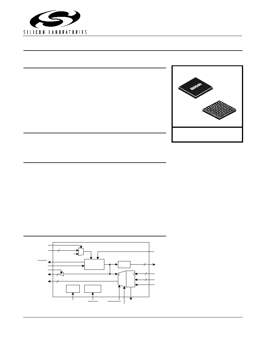
Functional Block Diagram
Data Rates Supported: OC-192/STM-64,
10GbE, and 10.7 Gbps FEC
Low Power Operation 0.6 W (typ)
Small Footprint: 99-Pin BGA Package
(11 x 11 mm)
DSPLLTM Based Clock Multiplier Unit
w/ selectable loop filter bandwidths
OIF SFI-4 Compliant Interface
Output Clock Powerdown
Operates with 155 or 622 MHz
Reference Sources
Optional 3.3 V Supply Pin for
LVTTL Compatible Outputs
Single 1.8 V Supply Operation
Sonet/SDH/ATM Routers
Add/Drop Multiplexers
Digital Cross Connects
Optical Transceiver Modules
Sonet/SDH Test Equipment
TXDO U T
TXDIN [15:0]
TXCL K16O U T
FIF O RST
F IFO ER R
16:
1
MU
X
FI
F
O
TXCL K16IN
TX M SBSEL
TXCL KO UT
TXSQ LC H
2
2
2
R EFC LK
TXLO L
D SPLL
TM
C M U
TXC LKD SBL
2
TXC LK16IN
R EFSEL
BW SEL
2
32
16
R EFRATE
B ias
R eset
Con trol
R EXT
RES ET
˜
Ordering Information:
See page 17.
Si5364
Bottom View
P
R E L I M I N A R Y
D
A TA
S
H E E T

S i 5 5 4 0
2
Preliminary Rev. 0.31

S i5540
Preliminary Rev. 0.31
3
T
A B L E
O F
C
O N T E N TS
Section
Page
Electrical Specifications . . . . . . . . . . . . . . . . . . . . . . . . . . . . . . . . . . . . . . . . . . . . . . . . . 4
Functional Description . . . . . . . . . . . . . . . . . . . . . . . . . . . . . . . . . . . . . . . . . . . . . . . . . . 9
DSPLLTM Clock Multiplier Unit . . . . . . . . . . . . . . . . . . . . . . . . . . . . . . . . . . . . . . . . . . 9
Reference Clock . . . . . . . . . . . . . . . . . . . . . . . . . . . . . . . . . . . . . . . . . . . . . . . . . . . . . 9
Serialization . . . . . . . . . . . . . . . . . . . . . . . . . . . . . . . . . . . . . . . . . . . . . . . . . . . . . . . . 9
Reset . . . . . . . . . . . . . . . . . . . . . . . . . . . . . . . . . . . . . . . . . . . . . . . . . . . . . . . . . . . . . 10
Clock Disable . . . . . . . . . . . . . . . . . . . . . . . . . . . . . . . . . . . . . . . . . . . . . . . . . . . . . . . 10
Bias Generation Circuitry . . . . . . . . . . . . . . . . . . . . . . . . . . . . . . . . . . . . . . . . . . . . . . 10
Differential Output Circuitry . . . . . . . . . . . . . . . . . . . . . . . . . . . . . . . . . . . . . . . . . . . . 11
Si5540 Pinout: 99-Pin BGA . . . . . . . . . . . . . . . . . . . . . . . . . . . . . . . . . . . . . . . . . . . . . . . 12
Pin Descriptions: Si5540 . . . . . . . . . . . . . . . . . . . . . . . . . . . . . . . . . . . . . . . . . . . . . . . . . 14
Ordering Guide . . . . . . . . . . . . . . . . . . . . . . . . . . . . . . . . . . . . . . . . . . . . . . . . . . . . . . . . . 17
Package Outline . . . . . . . . . . . . . . . . . . . . . . . . . . . . . . . . . . . . . . . . . . . . . . . . . . . . . . . . 18
Contact Information . . . . . . . . . . . . . . . . . . . . . . . . . . . . . . . . . . . . . . . . . . . . . . . . . . . . . 20

S i 5 5 4 0
4
Preliminary Rev. 0.31
Electrical Specifications
Figure 1. Differential Voltage Measurement (TXDIN, TXDOUT, TXCLK16IN, TXCLK16OUT)
Figure 2. Data to Clock Delay
Figure 3. Rise/Fall Time Measurement
Table 1. Recommended Operating Conditions
Parameter
Symbol
Test Condition
Min*
Typ
Max*
Unit
Ambient Temperature
T
A
≠40
25
85
∞
C
LVTTL Output Supply Voltage
V
DD33
1.71
--
3.47
V
Si5540 Supply Voltage
V
DD
1.71
1.8
1.89
V
*Note:
All minimum and maximum specifications are guaranteed and apply across the recommended operating conditions.
Typical values apply at nominal supply voltages and an operating temperature of 25
∞
C unless otherwise stated.
V
IS
V
ID
,V
OD
(V
ID
= 2V
IS
)
Differential
I/Os
Differential
Voltage Swing
Single Ended Voltage
Differential Peak-to-Peak Voltage
SIGNAL +
SIGNAL ≠
(SIGNAL +) ≠ (SIGNAL ≠)
V
ICM
, V
OCM
V
t
TXDOUT,
TXDIN
TXCLKOUT,
TXCLK16IN
t
CP
t
hd
t
su
t
CH
All Differential
IOs
t
F
t
R
80%
20%

S i5540
Preliminary Rev. 0.31
5
Table 2. DC Characteristics, V
DD
= 1.8 V
(V
DD
= 1.8 V ±5%, T
A
= ≠40∞C to 85∞C)
Parameter
Symbol
Test Condition
Min
Typ
Max
Unit
Supply Current
I
DD
--
333
TBD
mA
Power Dissipation
P
D
--
0.6
TBD
W
Common Mode Output Voltage
(TXDOUT,TXCLKOUT)
V
OCM
.8
0.9
1.0
V
Differential Output Voltage Swing
(TXDOUT,TXCLKOUT), Differential pk-pk
V
OD
See Figure 1
800
1000
1200
mV
(pk-pk)
LVPECL Input Voltage High (REFCLK)
V
IH
1.975
2.3
2.59
V
LVPECL Input Voltage Low (REFCLK)
V
IL
1.32
1.6
1.99
V
LVPECL Input Voltage Swing (REFCLK),
Differential pk-pk
V
ID
250
--
2600
mV
(pk-pk)
LVPECL Input Common Mode (REFCLK)
V
ICM
1.65
1.95
2.30
V
Input Impedance
(REFCLK, TXDIN, TXCLK16IN)
R
IN
Each input to
common mode
42
50
58
LVDS Input High Voltage (TXDIN,
TXCLK16IN)
V
IH
--
--
2.4
V
LVDS Input Low Voltage (TXDIN,
TXCLK16IN)
V
IL
0.0
--
--
V
LVDS Input Voltage, Single Ended pk-pk
(TXDIN, TXCLK16IN)
V
ISE
100
--
600
mV
(pk-pk)
LVDS Input Common Mode Voltage
(TXDIN, TXCLK16IN)
V
ICM
.8
2.0
2.4
V
LVDS Output High Voltage
(TXCLK16OUT)
V
OH
100
Load
Line-to-Line
TBD
--
1.475
V
LVDS Output Low Voltage
(TXCLK16OUT)
V
OL
100
Load
Line-to-Line
0.925
--
TBD
V
LVDS Output Voltage, Single Ended pk-pk
(TXCLK16OUT)
V
OSE
100
Load
Line-to-Line, See
Figure 1
250
400
550
mV
(pk-pk)
LVDS Output Common Mode Voltage
(TXCLK16OUT)
V
OCM
1.125
1.20
1.275
V
Output Short to GND
(TXCLK16OUT, TXDOUT, TXCLKOUT)
I
SC≠
--
25
TBD
mA
Output Short to V
DD
(TXCLK16OUT, TXDOUT, TXCLKOUT)
I
SC+
TBD
≠100
--
µ
A
LVTTL Input Voltage Low
(TXCLKDSBL, FIFORST, TXSQLCH,
BWSEL, REFRATE, REFSEL, TXMSBSEL,
RESET)
V
IL2
--
--
0.8
V