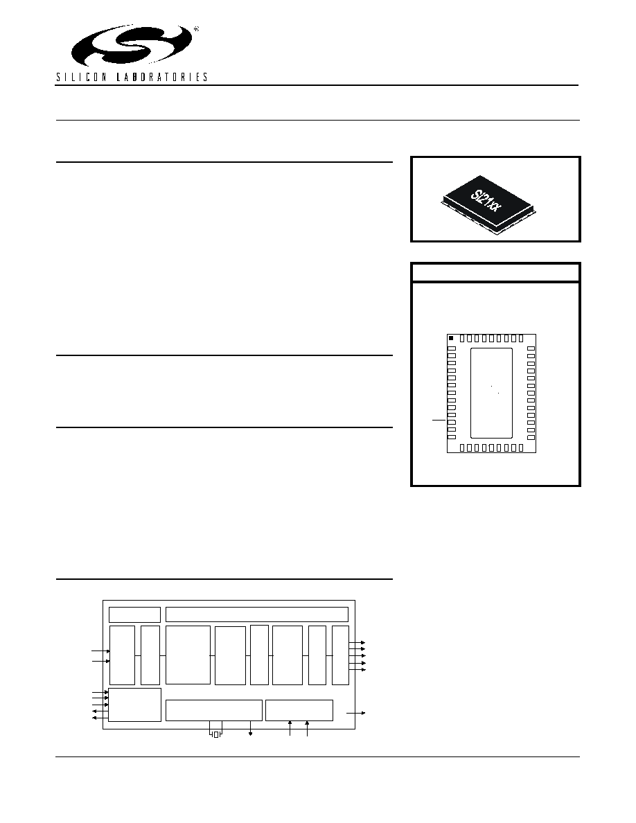
 | –≠–ª–µ–∫—Ç—Ä–æ–Ω–Ω—ã–π –∫–æ–º–ø–æ–Ω–µ–Ω—Ç: SI2108 | –°–∫–∞—á–∞—Ç—å:  PDF PDF  ZIP ZIP |
Preliminary Rev. 0.7 3/06
Copyright © 2006 by Silicon Laboratories
Si2107/08/09/10
This information applies to a product under development. Its characteristics and specifications are subject to change without notice.
Si2107/08/09/10
S
A T E L L I T E
R
E C E I V E R
F O R
DVB-S/DSS
Features
Applications
Description
The Si2107/08/09/10 are a family of pin-compatible, complete front-end solutions
for DSS and DVB-S digital satellite reception. The IC family incorporates a tuner,
demodulator, and LNB controller into a single device resulting in significantly
reduced board space and external component count. The device supports symbol
rates of 1 to 45 MBaud over a 950 to 2150 MHz range. A full suite of features
including automatic acquisition, fade recovery, blind scanning, performance
monitoring, and DiSEqC Level 2.2 compliant signaling are supported. The Si2108/
10 further add short circuit protection, overcurrent protection, and a step-up dc-dc
controller to implement a low-cost LNB supply solution. Si2110/09 versions
include a hardware channel scan accelerator for fast "blindscan". An I2C bus
interface is used to configure and monitor all internal parameters.
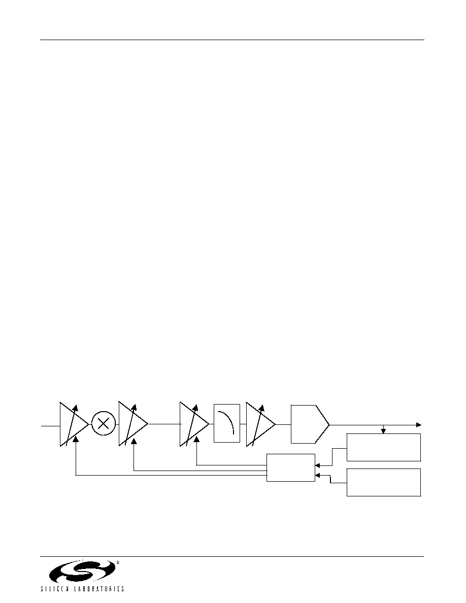
Functional Block Diagram
Single-chip tuner, demodulator,
and LNB controller
DVB-S- and DSS-compliant
QPSK/BPSK demodulation
Integrated step-up dc-dc
converter for LNB power supply
(Si2108/10 only)
Input signal level:
≠81 to ≠18 dBm
Symbol rate range:
1 to 45 MBaud
Automatic acquisition and fade
recovery
Automatic gain control
On-chip blind scan accelerator
(Si2109/10 only)
DiSEqCTM 2.2 support
Power, C/N, and BER estimators
I2C bus interface
3.3/1.8 V supply, 3.3 V I/O
Lead-free/RoHS-compliant
package
Set-top boxes
Digital video recorders
Digital televisions
Satellite PC-TV
SMATV trans-modulators
(Satellite Master Antenna TV)
Acquisition Control
AGC
Tuner
A/D
Con
v
er
ter
Demodulator
Viterbi
Decoder
De
-in
t
erle
ave
r
RS
Decoder
Des
c
ramb
le
r
MP
E
G
-
T
S
LNB Control
RF Sythesizer
I2C Interface
XOUT
SCL SDA
INT/RLK/GPO
TS_ERR
TS_SYNC
TS_VAL
TS_DATA[7:0]
TS_CLK
PWM/DCS
ISEN/NC
LNB2/DRL
VSEN/TDET
RFIP
LNB1/TGEN
Pin Assignments
Si2107/08/09/10
14 15 16 17 18 19 20 21 22
36
37
38
39
40
41
42
43
44
VD
D
_
SY
N
T
H
VD
D
_
L
O
GN
D
RF
IP
1
RF
IN
1
RF
IN
2
RF
IP
2
VDD_LNA
REXT
ADDR
VDD_MIX
VDD_BB
VDD_ADC
VSEN/TDET
LNB1/TGEN
ISEN
PWM/DCS
VDD_DIG18
T
S
_
D
AT
A[
1
]
TS_DATA[7]
T
S
_C
LK
SCL
SDA
TS_SYNC
TS_VAL
TS_ERR
INT/RLK/GPO
VDD_PLL33
XTOUT
VDD_XTAL
XTAL2
XTAL1
RESET
LNB2/DRC
T
S
_
D
AT
A[
0
]
T
S
_
D
AT
A[
3
]
T
S
_
D
AT
A[
2
]
T
S
_
D
AT
A[
4
]
T
S
_
D
AT
A[
5
]
TS_DATA[6]
VD
D
_
D
I
G
3
3
VD
D
_
D
I
G
3
3
GN
D
GN
D
Top
View
1
2
3
4
5
6
7
8
9
10
11
12
13
23
24
25
26
27
28
29
30
31
32
33
34
35
GND
GND

Si2107/08/09/10
2
Preliminary Rev. 0.7

Si2107/08/09/10
Preliminary Rev. 0.7
3
T
A B L E
O F
C
O N T E N TS
Section
Page
1. Electrical Specifications . . . . . . . . . . . . . . . . . . . . . . . . . . . . . . . . . . . . . . . . . . . . . . . . . . .4
2. Typical Application Schematic . . . . . . . . . . . . . . . . . . . . . . . . . . . . . . . . . . . . . . . . . . . . .10
3. Bill of Materials . . . . . . . . . . . . . . . . . . . . . . . . . . . . . . . . . . . . . . . . . . . . . . . . . . . . . . . . . .13
4. Part Versions . . . . . . . . . . . . . . . . . . . . . . . . . . . . . . . . . . . . . . . . . . . . . . . . . . . . . . . . . . .16
5. Functional Description . . . . . . . . . . . . . . . . . . . . . . . . . . . . . . . . . . . . . . . . . . . . . . . . . . .17
5.1. Tuner . . . . . . . . . . . . . . . . . . . . . . . . . . . . . . . . . . . . . . . . . . . . . . . . . . . . . . . . . . . . .17
5.2. Demodulator . . . . . . . . . . . . . . . . . . . . . . . . . . . . . . . . . . . . . . . . . . . . . . . . . . . . . . .17
5.3. DVB-S/DSS Channel Decoder . . . . . . . . . . . . . . . . . . . . . . . . . . . . . . . . . . . . . . . . .17
5.4. On-Chip Blindscan Accelerator (Si2109/10 Only) . . . . . . . . . . . . . . . . . . . . . . . . . . .18
5.5. LNB Signaling Controller . . . . . . . . . . . . . . . . . . . . . . . . . . . . . . . . . . . . . . . . . . . . . .18
5.6. On-Chip LNB DC-DC Step-Up Controller (Si2108/10 Only) . . . . . . . . . . . . . . . . . . .18
5.7. Crystal Oscillator . . . . . . . . . . . . . . . . . . . . . . . . . . . . . . . . . . . . . . . . . . . . . . . . . . . .18
6. Operational Description . . . . . . . . . . . . . . . . . . . . . . . . . . . . . . . . . . . . . . . . . . . . . . . . . . .19
6.1. System Configuration . . . . . . . . . . . . . . . . . . . . . . . . . . . . . . . . . . . . . . . . . . . . . . . .19
6.2. Interrupts . . . . . . . . . . . . . . . . . . . . . . . . . . . . . . . . . . . . . . . . . . . . . . . . . . . . . . . . . .20
6.3. Receiver Status . . . . . . . . . . . . . . . . . . . . . . . . . . . . . . . . . . . . . . . . . . . . . . . . . . . . .22
6.4. Tuning Control . . . . . . . . . . . . . . . . . . . . . . . . . . . . . . . . . . . . . . . . . . . . . . . . . . . . . .22
6.5. Channel Decoder . . . . . . . . . . . . . . . . . . . . . . . . . . . . . . . . . . . . . . . . . . . . . . . . . . .24
6.6. Automatic Gain Control . . . . . . . . . . . . . . . . . . . . . . . . . . . . . . . . . . . . . . . . . . . . . . .25
6.7. LNB Signaling Controller . . . . . . . . . . . . . . . . . . . . . . . . . . . . . . . . . . . . . . . . . . . . . .26
6.8. On-Chip LNB DC-DC Step-Up Controller (Si2108/10 Only) . . . . . . . . . . . . . . . . . . .28
7. I2C Control Interface . . . . . . . . . . . . . . . . . . . . . . . . . . . . . . . . . . . . . . . . . . . . . . . . . . . . .30
8. Control Registers . . . . . . . . . . . . . . . . . . . . . . . . . . . . . . . . . . . . . . . . . . . . . . . . . . . . . . . .31
9. Pin Descriptions . . . . . . . . . . . . . . . . . . . . . . . . . . . . . . . . . . . . . . . . . . . . . . . . . . . . . . . . .75
10. Ordering Guide1,2 . . . . . . . . . . . . . . . . . . . . . . . . . . . . . . . . . . . . . . . . . . . . . . . . . . . . . .78
11. Package Outline: 44-pin QFN . . . . . . . . . . . . . . . . . . . . . . . . . . . . . . . . . . . . . . . . . . . . .79
Document Change List . . . . . . . . . . . . . . . . . . . . . . . . . . . . . . . . . . . . . . . . . . . . . . . . . . . . .80
Contact Information . . . . . . . . . . . . . . . . . . . . . . . . . . . . . . . . . . . . . . . . . . . . . . . . . . . . . . . .82

Si2107/08/09/10
4
Preliminary Rev. 0.7
1. Electrical Specifications
Table 1. Recommended Operating Conditions
Parameter
Symbol
Min
Typ
Max
Unit
Ambient temperature
T
A
0
--
70
∞C
DC supply voltage, 3.3 V
V
3.3
3.0
3.3
3.6
V
DC supply voltage, 1.8 V
V
1.8
1.71
1.8
1.89
V
Note: All minimum and maximum specifications are guaranteed and apply across the recommended operating conditions.
Table 2. Absolute Maximum Ratings
1, 2
Parameter
Symbol
Min
Max
Unit
DC supply voltage, 3.3 V
V
3.3
≠0.3
3.9
V
DC supply voltage, 1.8 V
V
1.8
≠0.3
2.19
V
Input voltage - pins 2, 3, 7, 9, 11
V
IN
≠0.3
V
3.3
+ 0.3
V
Input current - pins 2, 3, 7, 9, 11
I
IN
≠10
+10
mA
Operating ambient temperature
T
OP
≠10
+70
∞C
Storage temperature
T
STG
≠55 150
∞C
RF input level
--
10
dBm
ESD protection - pins 39≠40, 42≠43
1
kV
ESD protection - pins 1≠38, 41, 44
2
kV
Notes:
1. Permanent damage may occur if the absolute maximum ratings are exceeded. Functional operation should be
restricted to the conditions as specified in the operations sections of this data sheet. Exposure to absolute maximum
rating conditions for extended periods may affect device reliability.
2. The Si2107/08/09/10 is a high-performance RF integrated circuit. Handling and assembly of these devices should
only be done at ESD-protected workstations.

Si2107/08/09/10
Preliminary Rev. 0.7
5
Table 3. DC Characteristics
(V
3.3
= 3.3 V ±10%, V
1.8
= 1.8 V ±10%, T
A
= 0≠70 ∫C)
Parameter
Symbol
Test Condition
Min
Typ
Max
Unit
Supply Current, 3.3 V
I
3.3
45 Msps, CR 7/8*
--
313
--
mA
20 Msps, CR 2/3*
--
298
--
mA
Supply Current, 1.8 V
I
1.8
45 Msps, CR 7/8*
--
292
--
mA
20 Msps, CR 2/3*
--
217
--
mA
Input high voltage
V
IH
SCL(25), SDA(26)
2.3
--
5.5
V
Input low voltage
V
IL
SCL(25), SDA(26)
0
--
0.8
V
Input leakage
I
I
SCL(25), SDA(26)
--
--
±10
µA
Output high voltage
V
OH
2.4
--
--
V
Output low voltage
V
OL
--
--
0.4
V
Output leakage
I
OL
--
--
±10
µA
*Note: LNB dc-dc converter disabled; LNB_EN (CEh[2]) = 0.
Table 4. RF Electrical Characteristics
Parameter
Symbol
Test Condition
Min
Typ
Max
Unit
Input power, single channel
P
i,ch
≠81
--
≠23
dBm
Aggregate input power
P
i,agg
--
--
≠7
dBm
Input impedance, balanced
Z
in
Z
SOURCE
= 75
--
75
--
Return Loss
--
≠10
--
dB
Dynamic voltage gain range
GV
--
75
--
dB
Maximum voltage gain
G
V(max)
--
55
--
dB
Noise figure
NF
Max gain
1
--
+9.5
+12.5
dB
IP3
IP3
2
Min gain
3
+5
+15
--
dBm
LO leakage
L
LO
950 to 2150 MHz
--
--
≠70
dBm
LO SSB phase noise
N
LO
100 kHz offset
--
≠97
≠94
dBc/Hz
1 MHz offset
--
≠97
≠94
dBc/Hz
LO DSB phase noise (integrated)
N
LO
10 kHz to 1/2 Baud
Rate
--
2.1
2.8
∞rms
RF synthesizer spurious
At 20 MHz offset
--
≠40
--
dBc/Hz
Reference oscillator phase noise
At 2 kHz offset
--
≠130
--
dBc/Hz
LO oscillator settling time
t
s,LO
--
100
--
µs
Notes:
1. Max gain = +55 dB.
2. IM3 can be calculated as follows: IM3 = 2 x (IP3 ≠ P
in
).
3. Min gain = ≠35 dB.

Si2107/08/09/10
6
Preliminary Rev. 0.7
Table 5. Receiver Characteristics
Parameter
Symbol
Test Condition
Min
Typ
Max
Unit
RF input frequency range
f
in
950
--
2150
MHz
Fine tune step size
f
step
--
125
--
kHz
Symbol rate range
R
S
1
--
45
MBaud
Carrier offset correction range
f
car_off
--
±6
--
MHz
Table 6. LNB Supply Characteristics (Si2108/10 Only)
Parameter
Symbol
Test Condition
Min
Typ
Max
Unit
Supply Voltage
V
LNB_IN
8
12
13.2
V
Converter Switch Frequency
237
264
290
kHz
Output HIGH voltage
VHIGH = 1010
17.75
18.625
19.5
V
VHIGH = 0000
17.0
18.0
19.0
V
Output LOW voltage
VLOW = 0110
12.75
13.375
14.0
V
VLOW = 0100
12.5
13.25
14.0
V
Low to High Transition Time
13 to 18 V
--
--
1
ms
High to Low Transition Time
18 to 13 V
--
--
1
ms
Line Regulation
V
CC
= 8 to
13.2 V
I
o
= 500 mA
--
--
200
mV
Load Regulation
I
o
= 50 to
500 mA
V
CC
= 12 V
--
--
200
mV
Load Capacitance Tolerance
DiSEqC 1.x
--
--
0.75
µF
DiSEqC 2.x
--
--
0.25
µF
Output current limiting
ILIM = 00
400
--
550
mA
ILIM = 01
500
--
650
mA
ILIM = 10
650
--
850
mA
ILIM = 11
800
--
1000
mA
Maximum LNB Supply Current
IMAX = 01
1.4
1.6
1.92
A
Tone Frequency
f
tone
20
22
24
kHz
Tone Amplitude
500
650
800
mV
Tone Duty Cycle
40
50
60
%
Tone Rise and Fall Time
3
6
10
µs
Tone Detector Frequency Capture
Range
17.6
--
26.4
kHz
Tone Detector Input Amplitude
200
--
1000
mV
pp
Note: Specifications based on recommended schematics in Figure 5 and Figure 6.

Si2107/08/09/10
Preliminary Rev. 0.7
7
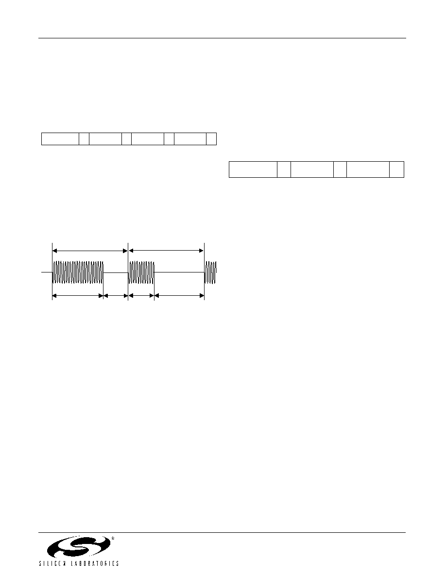
Figure 1. I
2
C Timing Diagram
Table 7. I2C Bus Characteristics
Parameter
Symbol
Test Condition
Min
Typ
Max
Unit
SCL Clock Frequency
f
SCL
0
--
400
kHz
Bus Free Time between START and
STOP Condition
t
BUF
1.3
--
--
µs
Hold Time (repeated) START Condition.
(After this period, the first clock pulse is
generated.)
t
HD, STA
0.6
--
--
µs
LOW Period of SCL Clock
t
LOW
1.3
--
--
µs
HIGH Period of SCL Clock
t
HIGH
0.6
--
--
µs
Data Setup Time
t
SU, DAT
100
--
--
ns
Data Hold Time
t
HD, DAT
0
--
0.9
µs
SCL and SDA Rise and Fall Time
t
r,
t
f
--
--
300
ns
Setup Time for a Repeated START Con-
dition
t
SU, STA
0.6
--
--
µs
Setup Time for STOP Condition
t
SU,STO
0.6
--
--
µs
Capacitive Load for each Bus Line
C
B
--
--
400
pF
SDA
SCL
t
f
S
t
LOW
t
HD;STA
t
r
t
HIGH
t
SU;DAT
t
f
t
HD;DAT
t
SU;STA
S
r
t
SP
t
HD;STA
t
SU;STO
t
BUF
t
r
P
S

Si2107/08/09/10
8
Preliminary Rev. 0.7
Figure 2. MPEG-TS (Rising Launch and Capture) Timing Diagram
Table 8. MPEG-TS Specifications (Rising Launch and Capture)
Parameter
Symbol
Test Condition
Min
Typ
Max
Unit
Clock cycle time
t
cycle
Serial mode
11.3
--
28.6
ns
Parallel mode
77
--
8000
ns
Clock low time
t
clow
Serial mode (TSSCR = 11)
5.1
--
6.9
ns
Serial mode (TSSCR = 00)
12.0
--
15.8
ns
Parallel mode
39
--
4000
ns
Clock high time
t
chigh
Serial mode (TSSCR = 01)
5.1
--
6.9
ns
Serial mode (TSSCR = 11)
12.0
--
15.8
ns
Parallel mode
39
--
4000
ns
Hold time
t
hold
Normal operation
--
0
--
ns
Data delayed (TSDD = 1)
--
1.5
--
ns
Clock Delayed (TSCD = 1)
--
≠1.5
--
ns
Setup time
t
setup
Normal operation
--
t
cycle
≠ 1.5
--
ns
Data delayed (TSDD = 1)
--
t
cycle
≠ 3.0
--
ns
Clock Delayed (TSCD = 1)
--
t
cycle
--
ns
Access time
t
access
--
1.5
--
ns
TS_CLK
TS_DATA
t
cycle
t
hold
t
setup
t
access
L
C

Si2107/08/09/10
Preliminary Rev. 0.7
9
Figure 3. MPEG-TS (Rising Launch, Falling Capture) Timing Diagram
Table 9. MPEG-TS Specifications (Rising Launch, Falling Capture)
Parameter
Symbol
Test Condition
Min
Typ
Max
Unit
Clock cycle time
t
cycle
Serial mode
11.3
--
28.6
ns
Parallel mode
77
--
8000
ns
Clock low time
t
clow
Serial mode (TSSCR = 11)
5.1
--
6.9
ns
Serial mode (TSSCR = 00)
12.0
--
15.8
ns
Parallel mode
39
--
4000
ns
Clock high time
t
chigh
Serial mode (TSSCR = 01)
5.1
--
6.9
ns
Serial mode (TSSCR = 11)
12.0
--
15.8
ns
Parallel mode
39
--
4000
ns
Hold time
t
hold
Normal operation
--
t
cycle
/2
--
ns
Data delayed (TSDD = 1)
--
t
cycle
/2 + 1.5
--
ns
Clock Delayed (TSCD = 1)
--
t
cycle
/2 ≠ 1.5
--
ns
Setup time
t
setup
Normal operation
--
t
cycle
/2 ≠ 1.5
--
ns
Data delayed (TSDD = 1)
--
t
cycle
/2 ≠ 3.0
--
ns
Clock Delayed (TSCD = 1)
--
t
cycle
/2
--
ns
Access time
t
access
--
1.5
--
ns
TS_CLK
TS_DATA
t
cycle
t
hold
t
setup
t
access
L
C
L
Si2107/08/09/10
10
Preliminary Rev. 0.7
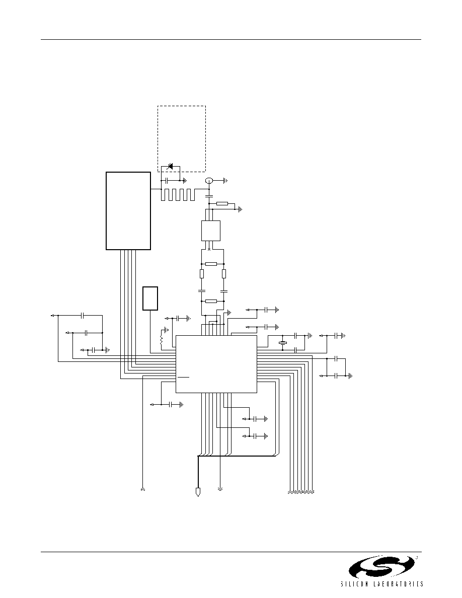
2. Typical Application Schematic
PWM
LNB2
ISEN
LNB1
VSEN
TS_DATA[7:0]
VCC3_3
VCC3_3
VCC1_8
VCC3_3
VCC3_3
VCC3_3
VCC3_3
VCC3_3
VCC3_3
VCC1_8
VCC3_3
TS_CLK
RESET
TS_VAL
TS_ERR
INT
XTOUT
SDA
SCL
TS_SYNC
LNB Supply Circuit (Si2108/10 only)
or
External LNB Controller
Address Select
See table 16
NOTE: Balun matching components are placeholders only.
Actual values, if necessary, to be determined with specific
layout and balun.
NOTE: Transient voltage suppression device.
Part number and type to be dictated by
surge requirements for the design.
NOTE: Trace length to be 1/4
wavelength at midband. It is
recommended that provision
be allowed for tuning of the
capacitor placement.
For highest performance, please submit layout for review by
Silicon Laboratories before PCB fabrication.
C2
C2
TC2
TC2
C14
C14
IN
2
NC
5
GND
1
OUT2
6
GND
3
OUT1
4
X1
BALUN TRANSFORMER
X1
BALUN TRANSFORMER
C36
C36
C8
C8
VDD_SYNTH
36
VDD_LO
37
GND
38
RFIP1
39
RFIN1
40
GND
41
RFIN2
42
RFIP2
43
GND
44
VDD_LNA
1
REXT
2
ADDR
3
VDD_MIX
4
VDD_BB
5
VDD_ADC
6
TD
ET/VSEN
7
DRC/LNB2
10
NC/ISEN
9
TGE
N/LNB
1
8
RESET
11
DCS/PWM
12
VDD_DIG18
13
TS_DATA0
14
TS_DATA1
15
TS_DATA2
16
TS_DATA3
17
VDD_DIG33
18
TS_CLK
19
VDD_DIG33
20
TS_DATA4
21
TS_DATA5
22
TS
_DATA6
23
TS
_DATA7
24
SCL
25
SDA
26
VDD_PLL33
31
TS_VAL
28
XTAL1
35
XTAL2
34
XTOUT
32
VDD_XTAL
33
INT/RLK/GPO
30
TS_SYNC
27
TS_ERR
29
U1
Si2107/8/9/10
U1
Si2107/8/9/10
C6
C6
TC3
TC3
TC1
TC1
1
3
Y1
Y1
1
2
J1
J1
C7
C7
D4
D4
C5
C5
C15
C15
C3
C3
C9
C9
C11
C11
R2
R2
TC5
TC5
C19
C19
C4
C4
C12
C12
C13
C13
C10
C10
TC4
TC4
C1
C1
C16
C16
F
i
gu
re
4.
Si2
107
/08/09
/1
0 Sche
mat
i
c

Si2107/08/09/10
Preliminary Rev. 0.7
11
LNB
VLNB_IN
VLNB_IN
For highest performance, please submit layout for review by
Silicon Laboratories before PCB fabrication.
C31
C31
R13
R13
R14
R14
Q6
Q6
C33
C33
R15
R15
Q1
Q1
C32
C32
R9
R9
Q4
Q4
R17
R17
D3
D3
R5
R5
R7
R7
Q3
Q3
R20
R20
Q5
Q5
R8
R8
R6
R6
C34
C34
L2
L2
PWM
12
ISEN
9
LNB2
10
LNB1
8
VSEN
7
Si2110 LNB Control
Si2110 LNB Control
D1
D1
R16
R16
R12
R12
R10
R10
R11
R11
C30
C30
Q2
Q2
Figure
5
.
D
iSEq
C 1.x LNB
Su
pply Circ
uit

Si2107/08/09/10
12
Preliminary Rev. 0.7
LNB
VLNB_IN
VLNB_IN
For highest performance, please submit layout for review by
Silicon Laboratories before PCB fabrication.
Q1
Q1
Q2
Q2
L3
L3
C30
C30
R14
R14
R9
R9
R13
R13
C31
C31
R11
R11
Q3
Q3
R12
R12
L2
L2
R16
R16
D1
D1
R18
R18
R20
R20
C17
C17
C33
C33
R15
R15
R8
R8
C32
22 nF
C32
22 nF
Q5
Q5
R7
R7
PWM
12
ISEN
9
LNB2
10
LNB1
8
VSEN
7
Si2110 LNB Control
Si2110 LNB Control
Q4
Q4
R10
R10
D3
D3
R5
R5
C35
C35
R6
R6
Q6
Q6
C34
C34
R17
R17
Figure
6
.
D
iSEq
C 2.x LNB
Su
pply Circ
uit

Si2107/08/09/10
Preliminary Rev. 0.7
13
3. Bill of Materials
Table 10. Si2107/08/09/10 Bill of Materials
Component
Description
Vendor
C1,C2,C4,C6,C10,C8,C9,
C10,C13,C14,C15,C16
0.1 µF, X7R, ±20%
C5
0.01 µF, X7R, ±20%
C3,C7,C11,C12
33 pF, 6 V, NP0, ±10%
C19,C36
33 pF, 50 V, NP0, ±10%
D4
Transient voltage suppressor, 20 V
2
Littlefuse SMCJ20CA
J1
Connector, F-type, 75
, 950-2150 MHz
R2
4.53 k
, 62.5 mW, ±1%
TC1-5
See Note 1
X1
Balun transformer
Anaren B0922J7575A00
Y1
20 MHz, 20 pF, 50 ppm, 20
ESR
U1
Si2107/08/09/10
Silicon Laboratories
Notes:
1. Tuning component values depend on the balun selected and layout. Contact Silicon Laboratories for
assistance reviewing layouts and selecting matching components.
2. The transient voltage suppression device should be selected to match the surge requirements of the
application.

Si2107/08/09/10
14
Preliminary Rev. 0.7
Table 11. DiSEqC 1.x LNB Supply Bill of Materials (Si2108/10 Only)
Component
Description
Vendor
C30
47 µF, 25 V,Electrolytic,± 20%
C31
0.47 µF, 25 V, X7R,± 20%
C32
22 nF, 25 V, X7R, ± 20%
C33
0.22 µF, 25 V, X7R, ± 20%
C34
4.7 µF, 25 V, X7R, ± 20%
D1
CMPSH1-4, 40 V, 1 A
ZHCS750TA, 40 V, 750 mA
Central Semiconductor
Zetex
D3
MMBD1705, Dual diode, 20 V, 25 mA
Fairchild
L2
DR78098,33 µH,1.2 A, 20%
SD0705-330K-R-SL
Datatronic
ACT
Q1
ZXMN3B14
FDN337N
Zetex
Fairchild
Q2
FMMT618
Zetex
Q3,Q5,Q6
MMBT3904
Fairchild
Q4
FMMT718
Zetex
R5
1.3
, 500 mW, ±5%
R6
33
, 250 mW, ±5%
R7
10 k
, 62.5 mW, ±5%
R8
1 k
, 250 mW, ±5%
R9
680
, 125 mW, ±5%
R10
0.22
, 1 W, ±5%
R11
22 k
, 62.5 mW, ±1%
R12,R20
20 k
, 62.5 mW, ±5%
R13
33
, 62.5 mW, ±5%
R14
43 k
, 62.5 mW, ±5%
R15
3 k
, 100 mW, ±5%
R16
2 k
, 250 mW, ±5%
R17
2.2 k
, 62.5 mW, ±1%

Si2107/08/09/10
Preliminary Rev. 0.7
15
Table 12. DiSEqC 2.x LNB Supply Bill of Materials (Si2108/10 Only)
Component
Description
Vendor
C17
1200 pF, 25 V, X7R, ± 20%
C30
47 µF, 25 V,Electrolytic,± 20%
C31,C35
0.47 µF, 25 V, X7R,± 20%
C32
22 nF, 25 V, X7R, ± 20%
C33
0.22 µF, 25 V, X7R, ± 20%
C34
4.7 µF, 25 V, X7R, ± 20%
D1
CMPSH1-4, 40 V, 1 A
ZHCS750TA, 40 V, 750 mA
Central Semiconductor
Zetex
D3
MMBD1705, Dual diode, 20 V, 25 mA
Fairchild
L2
DR78098,33 µH,1.2 A, 20%
SD0705-330K-R-SL
Datatronic
ACT
L3
DR78097,100 µH, 500 mA, 20%
SD0504-101K-R-SL
Datatronic
ACT
Q1
ZXMN3B14
FDN337N
Zetex
Fairchild
Q2
FMMT618
Zetex
Q3,Q5,Q6
MMBT3904
Fairchild
Q4
FMMT718
Zetex
R5
1.3
, 500 mW, ±5%
R6
33
, 250 mW, ±5%
R7
10 k
, 62.5 mW, ±5%
R8
1 k
, 250 mW, ±5%
R9
680
, 125 mW, ±5%
R10
0.22
, 1 W, ±5%
R11
22 k
, 62.5 mW, ±1%
R12,R20
20 k
, 62.5 mW, ±5%
R13
33
, 62.5 mW, ±5%
R14
43 k
, 62.5 mW, ±5%
R15
3 k
, 100 mW, ±5%
R16
2 k
, 250 mW, ±5%
R17
2.2 k
, 62.5 mW, ±1%
R18
16
, 250 mW, ±5%

Si2107/08/09/10
16
Preliminary Rev. 0.7
4. Part Versions
There are four pin- and software-compatible versions of
this device. All versions include the L-band tuner, DVB-
S/DSS demodulator and channel decoder, and LNB
signaling controller. Furthermore, the Si2108 and
Si2110 integrate an efficient LNB supply regulator while
allowing operation with an external LNB supply
regulator circuit. The LNB supply controller utilizes a
step-up converter architecture. In case operation with
an external regulator is desired, Si2107 and Si2109 can
be used; these do not integrate the LNB step-up dc-dc
controller.
On the other hand, the Si2109 and Si2110 integrate an
on-chip "blindscan" accelerator, which allows the
implementation of a very fast channel scan, an
important feature for end products targeted to free-to-air
(FTA) applications in which channel locations are
unknown. Si2107 and Si2108 do not integrate this
accelerator and are a good fit when symbol rates and
frequencies of satellite channels are known, as in the
case of pay-TV receivers or for FTA receivers in which
the embedded firmware contains the channel tuning
information. Table 13 summarizes the differences
between part versions.
Table 13. Device Versions
Part
Number
DVB-S/DSS
Integrated Tuner/
Demodulator with
Integrated LNB
Messaging
LNB Supply
Regulator
On-Chip
Blindscan
Accelerator
Si2110
Y
Y
Y
Si2109
Y
N
Y
Si2108
Y
Y
N
Si2107
Y
N
N

Si2107/08/09/10
Preliminary Rev. 0.7
17
5. Functional Description
The Si2107/08/09/10 is a family of highly-integrated
CMOS RF satellite receivers for DVB-S and DSS
applications. The device is an ideal solution for satellite
set-top boxes, digital video recorders, digital televisions,
and satellite PC-TV. The IC incorporates a tuner,
demodulator, and LNB controller into a single device
resulting in a significant reduction in board space and
external component count. The device supports symbol
rates of 1 to 45 Msym/s over a 950 to 2150 MHz range.
A full suite of features including automatic acquisition,
fade recovery, blind scanning, performance monitoring,
and DiSEqCTM Level 2.2 compliant signaling are
supported. The Si2110 and Si2108 further add short-
circuit protection, overcurrent protection, and a step-up
dc-dc controller to implement a low-cost LNB supply.
Furthermore, the Si2109 and Si2110 have an on-chip
blindscan accelerator. An I2C bus interface is used to
configure and monitor all internal parameters.
5.1. Tuner
The tuner is designed to accept RF signals within a 950
to 2150 MHz frequency range. The inputs are matched
to a 75
coaxial cable in a single-ended configuration.
The tuner block consists of a low-noise amplifier (LNA),
variable gain attenuators, a local oscillator, quadrature
downconverters, and anti-aliasing filters. The LNA and
variable gain stages provide balance between the noise
figure and linearity characteristics of the system. When
all gain stages are combined, the device provides more
than 80 dB of gain range. The desired tuning frequency
can be adjusted in intervals of 125 kHz, without the aid
of external varactors, using a unique two-stage tuning
algorithm that is supplied with the software driver. The
rapid settling time of the local oscillator improves
channel acquisition and switching performance. The
PLL loop filter has been completely integrated into the
device resulting in low tuner phase noise, improved
spurious response, and reduced BOM cost. An external
20 MHz crystal unit generates the reference frequency
for the system.
5.2. Demodulator
The demodulator supports QPSK and BPSK
demodulation of channels between 1 to 45 Msym/s. It
incorporates the following functional blocks: analog-to-
digital converters (ADCs), dc notch filters, I/Q imbalance
corrector, decimation filters, matched filters, equalizer,
digital automatic gain controls, and a soft-decision
decoder. The demodulator supports rapid channel
acquisition using an advanced carrier offset estimation
algorithm. When combined with the Si2209/10's blind
scanning capabilities, the device becomes an ideal
solution for the free-to-air (FTA) and common interface
(CI) market. Automatic acquisition and fade recovery
sequencers are also included to reduce the required
amount of software interaction and to simplify the
overall design. The output of the demodulator is
quantized into a 4-bit number by the soft-decision
decoder. The use of soft-decision decoding improves
the error correction capabilities of the channel decoder.
5.3. DVB-S/DSS Channel Decoder
The Si2107/08/09/10 integrates a full-channel decoder,
which can be configured in either DSS or DVB-S mode
and consists of a soft-decision Viterbi decoder, de-
interleaver, Reed-Solomon decoder, and energy-
dispersal descrambler.
5.3.1. Viterbi decoder
The Viterbi decoder performs maximum likelihood
estimation of convolutional codes in compliance with
DVB-S and DSS standards. The decoder is capable of
detecting code rate, puncturing pattern phase, 90∞
phase rotation, and I/Q interchange. Supported code
rates are listed in Table 14
The device allows monitoring of the Viterbi bit-error rate
(BER) over a finite or infinite measurement window.
5.3.2. Convolutional De-Interleaver
The deinterleaver disassembles the Reed-Solomon
(RS) code words, which were interleaved by the
modulator, to provide better resilience against burst
errors. The Si2110/09 performs deinterleaving
according to DVB-S and DSS standards.
5.3.3. Reed-Solomon decoder
The Si2109/10 supports RS codes in compliance with
DVB-S and DSS specifications. Both standards use a
shortened Reed-Solomon code, which can correct up to
eight byte errors per information packet. DVB-S utilizes
204 byte codes. DSS utilizes 146 byte codes.
Table 14. Viterbi Code Rates
DVB-S
DSS
1/2
--
2/3
2/3
3/4
--
5/6
--
--
6/7
7/8
--

Si2107/08/09/10
18
Preliminary Rev. 0.7
The device allows monitoring of correctable bit,
correctable byte, and uncorrectable packet errors over a
finite or infinite measurement window. The device also
includes a total BER monitor, which compares received
data from a modulated PRBS sequence against the
same sequence generated from an on-chip PRBS
generator.
5.3.4. Energy-dispersal descrambler
The descrambler removes the energy dispersal
scrambling introduced by the DVB-S process. The
descrambler is automatically bypassed in DSS mode.
5.4. On-Chip Blindscan Controller
(Si2109/10 Only)
The device includes on-chip circuitry to facilitate
extremely fast detection of available satellite channels.
For each valid DVB-S/DSS channel, the tuning
frequency and symbol rate, which can be stored by the
host for subsequent tuning, are determined. On Si2107/
08 devices, the host needs to provide the channel
tuning frequency and symbol rate to the device.
5.5. LNB Signaling Controller
The device supports several LNB signaling methods
including dc voltage selection, continuous tone, tone
burst, DiSEqC 1.x- and DiSEqC 2.x-compliant
messaging, and several combinations of these to allow
simultaneous operation with legacy tone/burst and
DiSEqC-capable peripherals.
Si2107/09 includes the capability to convert I2C
signaling commands to signals that interface to an
external LNB supply regulator circuit. In the case of (bi-
directional) DiSEqC operation, the device modulates
(and demodulates) the PWK data to (and from) an
internal message FIFO, which the host uses to write
(and read) DiSEqC messages. In the case of
transmission, the device can generate either the 22 kHz
tone burst directly or generate a tone envelope for when
an external LNB supply controller is used, which
includes the 22 kHz oscillator.
5.6. On-Chip LNB DC-DC Step-Up Control-
ler (Si2108/10 Only)
Next to the LNB message signaling controller, the
device also integrates the LNB supply regulator
controller. The supported LNB supply regulator
architecture consists of a step-up dc-dc (boost)
converter followed by an efficient filter, linefeed, and
DiSEqC transmit/receive circuit, which implements a
very power-efficient LNB supply solution. This facilitates
a complete LNB supply circuit with only a minimal
number of external components.
5.7. Crystal Oscillator
The crystal oscillator requires a crystal with a resonant
fundamental frequency of 20 MHz to generate the
reference frequency for the local oscillator. A single
crystal can be shared between two devices by utilizing
the master-slave configuration shown in Figure 6.
Figure 6. Master-Slave Crystal Sharing
Si
21xx M
a
ste
r
Si2
1
xx
Sl
ave
XTOUT
XTAL2
XTAL1
Y1
C11
C12
XTAL1

Si2107/08/09/10
Preliminary Rev. 0.7
19
6. Operational Description
The following sections discuss the user-programmable
functionality offered by the corresponding register map
sections. Refer to Table 19, "Register Summary," on
page 31 and detailed register descriptions starting on
page 35.
6.1. System Configuration
The MPEG Transport Stream (TS) output interface
carries the decoded satellite data to external devices for
further processing. Both DVB-S and DSS receiver
modes and associated output data packet formats are
supported. Mode selection is controlled via the system
mode register, SYSM. QPSK or BPSK demodulation is
set via the modulation type (MOD) register.
The MPEG-TS output interface consists of the following
output pins:
TS_DATA[7:0]
Data
TS_CLK
Clock
TS_SYNC
Sync/Frame Start Indicator
TS_VAL
Valid Data Indicator
TS_ERR
Uncorrectable Packet Error
The start of a TS frame is indicated by the TS_SYNC
signal. The TS_SYNC signal is a pulse that is active
during the sync byte in a DVB-S frame or during the first
byte of a DSS frame and is active only while TS
synchronization exists. In serial mode, the TS_SYNC
pulse can be programmed to be active for the whole
byte, or the first bit only, by setting the TSSL bit. The
polarity of the TS_SYNC pulse can be programmed to
be either active high or active low using the TSSP bit.
The TS_VAL output is used to indicate when valid data
is present. TS_VAL is active during the MPEG-TS frame
packet data and inactive while parity data is being
output or when there is no TS synchronization. The
polarity of the TS_VAL output can be programmed to be
active high or active low using the TSVP bit.
The TS_ERR output indicates that an uncorrectable
error has been detected in the RS decoding stage and
that the current TS data packet contains uncorrectable
errors. The TS_ERR output is active during the entire
erred TS frame. The polarity of TS_ERR can be
programmed to be active high or active low using the
TSEP bit.
All signals on the MPEG-TS output interface can be
individually tri-stated using bits TSE_OE, TSV_OE,
TSS_OE, TSC_OE, and TSD_OE.
Transport stream data can be output in a parallel byte-
wide mode or a serial bit-wide mode for system-level
flexibility. Selection of the interface mode is controlled
via the TSM bit. In serial mode, data is output on
TS_DATA[0] while TS_DATA[7:1] are held low. The
direction of the serial data stream may be programmed
to output in an MSB or LSB first direction using the
TSDF bit. Parity data may be optionally zeroed by
setting the TSPG bit. To support board-level timing
modifications, the data stream may be delayed by
setting TSDD.
The transport stream clock can be programmed such
that data is transitioning on its rising or falling edge
using the TSCE bit. When operating in serial mode, the
transport stream clock mode bit, TSCM, can be used to
select either a gapped or continuous clock mode. In the
gapped mode, the clock is active only when data is
being output. For this, parity information is not
considered data when the TSPG is set to output zero
data during parity. In the continuous mode, the clock
runs without regard to data being output, and the user
uses TS_VAL as a data strobe. To support board-level
timing modifications, the clock stream may be delayed
by register bit TSCD.
In serial mode, the transport stream clock rate range is
determined by the TSSCR register. The exact rate is
determined during the acquisition process. The range
that minimizes the difference between the effective
transport stream data rate and the clock rate should be
chosen. The recommended settings are listed in
Table 15.
Figure 7 illustrates the parallel data mode. Figure 8
illustrates the continuous and gapped serial data
modes.
Table 15. Serial MPEG-TS Clock Frequency
TSSCR
Baud Rate
Serial Clock Rate
00
40≠50 Msps
80≠88.5 MHz
01
30≠40 Msps
76.8≠82.8 MHz
10
19≠30 Msps
54.9≠59.2 MHz
11
1≠19 Msps
35≠37.7 MHz
Si2107/08/09/10
20
Preliminary Rev. 0.7
Figure 7. MPEG-TS Parallel Mode
Figure 8. MPEG-TS Serial Modes
The device has one output pin (pin 30), which can be
configured as either a receiver lock indicator, general
purpose output, or interrupt output, using the pin select
register, PSEL. The receiver lock indicator provides a
signal output for register bit RCVL. The general purpose
output reflects the polarity of register bit GPO. The
interrupt output is discussed further in "6.2. Interrupts".
The user can configure the device such that
components of the channel decoder are bypassed. This
is controlled by the energy-dispersal descrambler
bypass bit, DS_BP, the Reed-Solomon decoder bypass
bit, RS_BP, and the convolutional de-interleaver bypass
bit, DI_BP. The use of these bypass options is defined
for the implementation of a BER test on a known
modulated PRBS data sequence as explained later in
"6.5. Channel Decoder" on page 24.
6.2. Interrupts
The device is equipped with several sticky interrupt bits
to provide precise event tracking and monitoring.
Next to interrupts being signaled via the I2C register
map, the user can program one of the device terminals
(INT) as a dedicated interrupt pin via the pin select
register bit, PSEL. The device contains an extensive
collection of interrupt sources that can be individually
masked from the INT pin using the corresponding
interrupt enable register bits, labeled with suffix "_E".
Thus, the INT output is a logical-OR of all enabled
interrupts. Generation of the channel interrupt on pin
INT can be masked off by using the interrupt enable bit,
INT_EN. Note that interrupt reporting in the register
map is not affected by INT_EN.
TS_DATA[7:0]
TS_SYNC active high
TS_VAL active high
TS_ERR active high
TS1 (sync)
TS2
Parallel Data Mode
TS_CLK, rising edge
TS188
TS1 (sync)
TS2
RS1
TS_CLK rising edge
Continuous Serial Data Mode
TS_DATA[0]
TS_VAL active low
TS_ERR, active low
TS188
RS1
TS1 (sync)
TS2
TS_CLK falling edge/ gapped
TS_DATA[0]
TS_SYNC active high
TS2
TS2
TS1 (sync)
TS1 (sync)
TS188
RS1
Gapped Serial Data Mode
TS2
TS1 (sync)
TS_SYNC, active low/1-bit wide
TS_VAL active high
TS_ERR active high

Si2107/08/09/10
Preliminary Rev. 0.7
21
The interrupt signal polarity can be configured to be
active high or active low using the interrupt polarity bit,
INTP. The interrupt signal type can be configured to be
CMOS output or open-drain/source output using the
interrupt type bit, INTT.
Interrupt bits are set by the device to 1 when an
interrupt occurs. The host clears an interrupt bit by
writing a 1 again, at which time the device resets the
interrupt bit to zero. Table 16 illustrates the interrupt
sources and their associated status, enable, and
interrupt bits.
Table 16. Events, Interrupts, and Status Bits
Event
Interrupt Bit
Enable Bit
Status Bit
Receiver lock
RCVL_I
RCVL_E
RCVL (0 ≠>1)
Receiver unlock
RCVU_I
RCVU_E
RCVL (1 ≠> 0)
Tuner lock
TUNL_I
TUNL_E
TUNL (0 ≠> 1)
AGC lock
AGCL_I
AGCL_E
AGCL (0 ≠> 1)
AGC threshold
AGCTS_I
AGCTS_E
AGCTS (0 ≠> 1)
Carrier estimation lock
CEL_I
CEL_E
CEL (0 ≠> 1)
Symbol rate estimation lock
SRL_I
SRL_E
SRL (0 ≠> 1)
Symbol timing lock
STL_I
STL_E
STL (0 ≠> 1)
Symbol timing unlock
STU_I
STU_E
STL (1 ≠> 0)
Carrier recovery lock
CRL_I
CRL_E
CRL (0 ≠> 1)
Carrier recovery unlock
CRU_I
CRU_E
CRL (1 ≠> 0)
Viterbi lock
VTL_I
VTL_E
VTL (0 ≠> 1)
Viterbi unlock
VTU_I
VTU_E
VTL (1 ≠> 0)
Frame synchronizer lock
FSL_I
FSL_E
FSL (0 ≠> 1)
Frame synchronizer unlock
FSU_I
FSU_E
FSL (1 ≠> 0)
Acquisition fail
AQF_I
AQF_E
AQF (0 ≠> 1)
C/N measurement complete
CN_I
CN_E
CNS (1 ≠> 0)
Viterbi BER measurement complete
VTBR_I
VTBR_E
VTBRS (1 ≠> 0)
RS measurement complete
RSER_I
RSER_E
RSERS (1 ≠> 0)
Message FIFO empty
FE_I
FE_E
FE (0 ≠> 1)
Message FIFO full
FF_I
FF_E
FF (0 ≠> 1)
Message received
MSGR_I
MSGPE_E
MSGR (0 ≠> 1)
Message parity error
MSGPE_
MSGR_
MSGPE (0 ≠> 1)
Message receive timeout
MSGTO_I
MSGTO_E
MSGTO (0 ≠> 1)
Short-circuit detect
SCD_I
SCD_E
SCD (0 ≠> 1)
Overcurrent detect
OCD_I
OCD_E
OCD (0 ≠> 1)
Si2107/08/09/10
22
Preliminary Rev. 0.7
6.3. Receiver Status
During receive operation, the host can retrieve
information on the status of AGC lock (AGCL), carrier
estimation lock (CEL), symbol rate estimation lock
(SRL), symbol timing lock (STL), carrier recovery lock
(CRL), Viterbi decoder lock (VTL), frame sync lock
(FSL), and overall receiver lock (RCVL).
During channel acquisition, the host can retrieve
information on error conditions due to: AGC search
(AGCF), carrier estimation (CEF), symbol rate search
(SRF), symbol timing search (STF), carrier recovery
search (CRF), Viterbi code rate search (VTF), frame
sync search (FSF), and overall receiver acquisition
(AQF),
6.4. Tuning Control
The Si2107/08/09/10 utilizes a unique two-stage tuning
algorithm to provide optimal RF reception. The input
signal is first mixed down to a low-IF frequency by a
coarse tuning stage and then down to baseband by a
fine-tune mixer. The user programs both coarse and
fine-tuning frequencies using the CTF and FTF
registers.
An algorithm (supplied with the reference software
driver) is used to automatically calculate the required
values. As part of the tuning process, the sample rate,
fs, should also be programmed via the ADCSR register.
Values between 192 and 207 MHz are supported. An
algorithm is supplied with the reference software driver
to automatically select the optimal sampling rate.
6.4.1. Automatic Acquisition
The receiver acquisition sequence consists of the
following stages: Analog AGC Search, Carrier Offset
Estimation, Symbol Rate Estimation, Symbol Timing
Recovery, Carrier Recovery, Viterbi Search, and Frame
Synchronization. For the receiver to lock, each stage
must run to completion or declare lock as shown in
Figure 9. If a given stage is unable to achieve lock after
exhausting a parameter search range or exceeding the
timeout period, it asserts a fail signal.
To initiate the acquisition sequence, the user should
program the acquisition start bit, AQS. All search
parameters must be specified before initiating the
acquisition. Upon completion of the acquisition
sequence, the AQS bit is automatically cleared. The
acquisition sequence can be aborted at any time by
clearing the AQS bit.
The status of the acquisition sequence can be
monitored via the registers in the receiver status register
map section. A successful acquisition is reported by the
assertion of the receiver lock bit, RCVL. A failed
acquisition is reported by the assertion of the acquisition
fail bit, AQF.
Figure 9. Acquisition Sequence (Symbol Rate
Estimation Available on Si2109/10 Only)
6.4.2. Carrier Offset Estimation
The desired carrier frequency may be offset from its
nominal position due to the imperfections and
temperature dependencies of the LNB. The carrier
offset estimator uses a search procedure to identify,
track, and remove this frequency offset from the system.
Seven different carrier offset estimation search ranges
can be programmed from 0.10 to ~6.0 MHz with register
CESR. Smaller search ranges result in faster search
times.
When carrier offset estimation is complete, the CEL bit
is asserted. If an error is detected during carrier offset
estimation, the CEF bit is set. Carrier offset estimation
commences under the control of the acquisition
Acquisition Start
Calibration
LO Tuning
Stage fail
done
lock
lock
lock
done
done
Analog AGC Search
CFO Estimation
1
Symbol Rate Estimation
1
Symbol Timing Loop
1
Carrier Frequency Loop
1
Viterbi Search
2
Frame Search
2
Receiver locked
Stage fail
Stage fail
and STL
unlocked
Stage fail
Stage fail
Stage fail
Stage fail but
STL is locked
1. Acquisition fail if stage fails n times in a row.
2. Acquisition fail if stage completes parameter range
without locking.

Si2107/08/09/10
Preliminary Rev. 0.7
23
sequencer.
After the completion of a search, the estimated carrier
offset is stored in the carrier frequency error register,
CFER. If no signal is found, the CEF bit is asserted. The
value contained in CFER may be optionally transferred
to the CFO register to adjust the search center
frequency and permit the utilization of a smaller search
range for subsequent acquisitions. This relationship can
be expressed by the following equation:
6.4.3. Symbol Rate Estimation (Si2109/10 Only)
The Si2109/10 supports the ability to automatically
detect the symbol rate of a channel when it is unknown.
This feature is ideal for FTA/CI applications where it is
often desirable to rapidly scan (blind scan) and detect
the available channels of a given satellite. If symbol rate
estimation is not required, the user should program the
symbol rate explicitly into the SR register. This is the
only mode of operation for Si2107/08.
On Si2109/10, the symbol rate unknown bit, SRUK, can
be changed from its default value to activate symbol
rate estimation. The search range must then be
bounded by programming the symbol rate maximum
and minimum registers, SRMX and SRMN. If the
symbol rate search is successful, the estimated symbol
rate is automatically written to the SR register. Smaller
search ranges result in faster search times. Note that
the values stored in the symbol rate, symbol rate
maximum, and symbol rate minimum registers are
sample rate-dependent. This relationship is described
by the following equation:
When symbol rate estimation is complete, the SRL bit is
asserted. If an error is detected during symbol rate
estimation, the SRF bit is also set. The symbol rate
estimator commences under the control of the
acquisition sequencer.
6.4.4. Carrier Recovery Loop
The carrier recovery loop is responsible for acquiring
frequency and phase lock to the incoming signal. When
lock is achieved, the carrier recovery lock indicator,
CRL, is asserted. If carrier recovery lock is not achieved
within a predefined timeout period, the device declares
carrier recovery failure by asserting the CRF bit. The
carrier recovery loop commences under the control of
the acquisition sequencer.
6.4.5. Symbol Timing Loop
The symbol timing recovery loop is responsible for
acquiring and tracking the symbol timing of the
incoming data signal. When lock is achieved, the
symbol timing loop lock indicator, STL, is asserted. If
symbol timing lock is not achieved within a predefined
timeout period, the device declares symbol timing loop
failure by asserting the STF bit. The symbol timing
recovery loop commences under the control of the
acquisition sequencer.
6.4.6. Automatic Fade Recovery
The device is designed to automatically recover lock in
the event of a fade condition. Fade recovery is
performed when any stage loses synchronization after
receiver lock has been achieved. It is assumed that
symbol rate, code rate, and puncturing pattern have not
changed; so, these parameters remain fixed during the
attempted reacquisition. The fade recovery sequence is
shown in Figure 10.
The fade recovery sequence continues until either
receiver lock is achieved or a new acquisition is
initiated.
Figure 10. Fade Recovery Sequence
Search center frequency
f
desired
CFO
+
f
s
2
15
--------
◊
Hz
=
Actual Symbol Rate
Symbol Rate
f
s
2
24
--------
◊
MHz
=
Unlock
lock
Done
Analog AGC Search
CFO Estimation
Symbol Timing Loop
Carrier Frequency Loop
Viterbi Search
(Limited)
Frame Search
Receiver locked
Fail
Calibration
LO Tuning
lock
lock
lock
Unlock
Unlock
Symbol Rate Estimation
Unlock
Unlock
Done

Si2107/08/09/10
24
Preliminary Rev. 0.7
6.4.7. C/N Estimator
A carrier-to-noise estimator is provided to aid in satellite
antenna positioning. The C/N measurement mode bit,
CNM, controls whether the count is performed over a
fixed-length or infinite window. With a fixed-length
window, the window size is defined by register CNW.
Measurements are stored in a 16-bit saturating register,
CNL. Setting the C/N estimator start bit, CNS clears the
CNL register and initiates the C/N measurement. When
operating in the finite window mode, the CNS bit is
automatically cleared when the measurement is
complete. The CNS bit must be cleared manually in the
infinite mode to stop the count. An external lookup table
is used to translate the measurement into a C/N
estimate for a given setting of the C/N threshold, CNET,
and a given digital AGC setting.
6.5. Channel Decoder
6.5.1. Viterbi Decoder
The Viterbi decoder performs maximum likelihood
estimation of convolutional codes in compliance with
DVB-S and DSS standards. When lock is achieved, the
Viterbi lock indicator, VTL, is asserted. If Viterbi lock is
not achieved after exhausting the specified parameter
space, the device declares Viterbi search failure by
asserting the VTF bit. The Viterbi search commences
under the control of the acquisition sequencer.
The device can be programmed to attempt to
automatically acquire Viterbi lock using all, one, or a
subset of the supported code rates using the VTCS
register.
If lock is achieved, the status of the search, including
code rate, puncturing pattern phase, 90-degree phase
rotation, and I/Q swap, can be monitored in the Viterbi
search status registers, VTRS, VTPS, and VTIQS.
6.5.2. Viterbi BER Estimator
The Viterbi BER estimator measures the frequency of
bit errors at the input of the Viterbi decoder. The Viterbi
BER mode bit, VTERM, controls whether the count is to
be performed over a fixed length or infinite window. The
window size is defined by VTERW. The BER count is
stored in a 16-bit saturating register, VTBRC. Setting
the Viterbi BER measurement start bit, VTERS, clears
the VTBRC register and initiates the measurement.
When operating in the finite window mode, the VTERS
bit is automatically cleared when the measurement is
complete. The VTERS bit must be cleared manually in
the infinite mode to stop the count.
6.5.3. Reed-Solomon Error Monitor
The Reed-Solomon error monitor is capable of counting
bit, byte, and uncorrectable packet errors. The error
type to be counted is controlled by the Reed-Solomon
error type register, RSERT. The Reed-Solomon error
mode bit, RSERM, controls whether the count is to be
performed over a fixed length or infinite window. The
window size is defined by RSERW. The BER count is
stored in a 16-bit saturating register, RSERC. Setting
the RS BER measurement start bit, RSERS, clears the
RSERC register and initiates the measurement. When
operating in the finite window mode, the RSERS bit is
automatically cleared when the measurement is
complete. The RSERS bit must be cleared manually in
the infinite mode, to stop the count.
6.5.4. PRBS BER Tester
To facilitate in-system pseudo random bit sequence
(PRBS) BER testing, the device provides the ability to
synchronize and track test sequences contained in the
payload (i.e. not SYNC bytes) of the MPEG data
stream. A PRBS test pattern must be encoded,
modulated, and injected into the channel to be
monitored. The device supports a PRBS 2
23
≠ 1 bits
long described by the following polynomial:
To enable PRBS testing, the Reed-Solomon error type
register, RSERT, must be appropriately programmed.
After the device has synchronized to the incoming
PRBS test pattern, errors are reported in the RSERC
register.
Measurements can be performed at the output of the
Viterbi or Reed-Solomon decoder. To record errors at
the output of the Viterbi decoder, the Reed-Solomon
decoder and interleaver must be bypassed by setting
RS_BP and DI_BP in the "System Configuration"
section of the register map. To record errors at the
output of the Reed-Solomon block, the RS_BP bit must
be cleared.
6.5.5. Frame Synchronizer
The output of the Viterbi decoder is aligned into bytes by
detecting sync patterns within the data stream. In DVB-
S systems, the sync byte, 47h, occurs during the first
byte of a 204 byte RS code block. In DSS systems, a
sync byte, 1Dh, is appended to the beginning of each
RS encoded 146-byte block, resulting in 147-byte RS
code blocks. In DSS mode, sync bytes are discarded
before the byte stream is output to subsequent
decoding stages. When lock is achieved, the frame
synchronization lock bit, FSL, is asserted. If lock is not
achieved, the frame synchronizer fail bit, FSF, is
asserted.
G x
( )
x
23
x
18
1
+
+
=
Si2107/08/09/10
Preliminary Rev. 0.7
25
The frame synchronizer commences under the control
of the acquisition sequencer.
Following frame synchronization lock, the device
examines the byte stream for a possible 180-degree
phase shift. If an inversion is detected, data are inverted
prior to being output.
6.6. Automatic Gain Control
The Si2107/08/09/10 is equipped with the ability to
adjust signal levels via an automatic gain control (AGC)
loop. This ensures that the noise and linearity
characteristics of the signal path are optimized at all
times. AGC settings can be set at 4 points in the analog
signal chain and 2 points in the digital signal chain.
6.6.1. Analog AGC
System gain is distributed into four independent stages
as shown in Figure 11. The gain range of all stages
combined is over 80 dB. When the AGC search
completes, the AGCL bit is asserted. If an error is
encountered during the AGC search, the AGCF bit is
also set. The AGC search commences under the
control of the acquisition sequencer.
The AGC loop works to automatically adjust the gain of
each stage to minimize the error between a measured
signal power and a desired output level. Signal power is
measured at the output of the ADC using an internal
rms power calculator. The result is stored in a 7-bit
saturating register, AGCPWR. The desired output level
is stored in the AGC threshold register, AGCTH. Signal
power measurements occur at a frequency dictated by
the AGC measurement window size, AGCW. This
frequency can be described using the following
equation, where fs equals the ADC sampling rate,
ADCSR.
When gain adjustments are made, the device allows up
to 100 µs for the gain changes to settle before
beginning the next measurement.
To facilitate a rapid initial acquisition, Si2107/08/09/10
includes an acquisition mode wherein the measurement
window size is reduced by a factor of 64 when
compared to the normal tracking mode.
During the AGC search, the device is in acquisition
mode, and the gain is adjusted until the measured
signal power crosses the desired threshold or a limit is
reached. If the signal power crosses the threshold
before reaching a limit, the search completes, and the
AGCL bit is asserted. If a gain limit is reached, the
device asserts both the AGCL bit and the AGCF bit.
In the normal tracking mode, the device continuously
measures the input signal power according to the AGC
measurement window size. If the absolute value of the
difference between the AGCTH and AGCPWR exceeds
the value of the AGC tracking threshold, AGCTR, the
AGC loop adjusts gain settings until the AGCPWR level
matches AGCTH.
The AGC gain offset register, AGCO, provides the
ability to apply a static gain offset to the input channel.
Silicon Laboratories will provide the recommended
values for this register. It is possible to read out the
instantaneous settings of each of the four VGAs from
the AGC<n>, <n = 1..4>, registers.
Figure 11. Analog AGC Control Loop
AGC measurement frequency
f
s
AGCW
------------------- Hz
=
LNA
VGA1
VGA2
OFFSET
A/D
AGC
rms calculator
AGC Threshold
LPF
MIXER

Si2107/08/09/10
26
Preliminary Rev. 0.7
6.6.2. Digital AGC
Downstream of the analog VGAs, after A/D conversion
of the signal, there are two points at which the digital
gain can be programmed. Digital AGC1 is used to
change signal power after removal of adjacent channels
by the (digital) anti-aliasing filter.
By default, DAGC1 is enabled and periodically adjusts
the gain of the I & Q data streams based on a
comparison of the measured complex RMS level and a
target value. The target value can be selected with the
DAGC1T register. Two levels are provided to allow
operation with additional headroom for signal peaks
during signal acquisition. The gain function of DAGC1
can be disabled using DAGC1_EN; then, no gain is
applied to I & Q data streams. The signal measurement
and gain adjustment normally operate continuously,
allowing the gain to track the input level. The
measurement window can be adjusted by register
DAGC1W. The automatic updating of the gain can be
frozen by register bit DAGC1HOLD. This holds the gain
to the last setting. The value of the gain can be read
from the DAGC1 register. It is possible to override the
internal AGC algorithm and provide host-based control
of AGC1 by appropriately programming register bit
DAGC1HOST.
Digital AGC2 (DAGC2) is intended to optimally scale the
soft decision outputs of the demodulator prior to Viterbi
decoding. This allows it to compensate for signal level
variations after matched filtering and equalization.
Normally, operation is continuous, but tracking can be
disabled using register bit DAGC2_TDIS. This holds the
gain to the last setting.
During AGC operation, the average power of the signal
is compared to a threshold set by register DAGC2T. The
signal power is measured over a finite window specified
by DAGC2W. The gain applied to the signal to make the
input match the programmed threshold can be read
from register DAGC2GA.
6.7. LNB Signaling Controller
All device versions provide LNB signaling capability.
The device supports several LNB signaling methods
including dc voltage selection, continuous tone, tone
burst, DiSEqC 1.x- and DiSEqC 2.x-compliant
messaging. A description of each method follows.
6.7.1. DC Voltage Selection
A constant dc voltage of 18 or 13 V is typically used to
switch the LNB between horizontal and vertical polarity
or clockwise and counterclockwise polarization. The
LNBV bit is used to select the desired voltage.
When an external LNB supply regulator is used, the
DCS pin is driven high or low depending on the
selection of high or low voltage.
6.7.2. Tone Generation
Tone-related information is communicated to external
devices via the TGEN pin. The tone format select bit,
TFS, specifies whether the output of TGEN is an
internally-generated tone or a tone envelope. The
frequency of the internal tone generator is governed by
the following equation:
Frequencies between 20 and 24 kHz are supported.
The default value of TFQ results in a nominal tone
frequency of 22 kHz. When tone envelope output is
selected, a high signal on TGEN corresponds to "tone
on" while a low signal corresponds to "tone off." When
operating in the "Manual LNB messaging mode", the TT
bit directly controls the output of the tone or tone
envelope.
6.7.2.1. Continuous Tone
A continuous tone is typically used to select between
the high and low band of an incoming satellite signal.
The LNBCT bit can be set to one to generate a
continuous tone.
6.7.2.2. Tone Burst
The tone burst signaling method can be used to
facilitate the control of a simple two-way switch. Two
types of tone burst are available, as shown in Figure 12.
An unmodulated tone burst persists for 12.5 ms. A
modulated tone burst lasts for the same duration but
consists of a sequence of nine 0.5 ms pulses and 1 ms
gaps. Tone burst selection is controlled via the LNBB
bit. The tone burst command can optionally be disabled
to support systems that do not use tone burst signaling
by setting the burst disable bit, BRST_DS, to one. This
disables the tone/burst generation as part of the
DiSEqC signaling sequence when the device uses
"Automatic LNB messaging mode" as described below.
Figure 12. Tone Burst Modulation
f
tone
100
32
TFQ 7:0
[
] 1
+
(
)
◊
[
]
---------------------------------------------------------- MHz
=
'0' Tone Burst (Satellite A)
Envelope
Envelope
Tone
12.5 ms
'1' Tone Burst (Satellite B)
Tone
Si2107/08/09/10
Preliminary Rev. 0.7
27
6.7.3. DiSEqCTM
The DiSEqC signaling method extends the functionality
of the legacy 22 kHz tone by superimposing a
command protocol and adding an optional return
channel. A DiSEqC command normally consists of a
framing byte, an address byte, a command byte, and,
optionally, one or more data bytes. This format is
illustrated in Figure 13.
Figure 13. DiSEqC Message Format
The length of a message is specified by MSGL. When
the message length is set to one byte, the message is
modulated using tone burst modulation. When the
message length is set to two or more bytes, the
message is modulated using DiSEqC-compliant
modulation, and the odd parity bit is automatically
added. The DiSEqC modulation scheme is illustrated in
Figure 14.
Figure 14. DiSEqC Compliant Modulation
6.7.3.1. DiSEqC 1.x One-Way Communication
Messages are programmed directly into the device
using a message FIFO that consists of six byte wide
registers, FIFO1≠6. The messages must be written in a
first-in-first-out manner such that the first byte of a
message is stored in FIFO1; the second byte is stored
in FIFO2, and so on. If messages are longer than six
bytes, the device asserts the FIFO empty indicator, FE,
as soon as the sixth byte has been read. The LNB
control module then takes its next byte from FIFO1 and
continues the process. The message length must also
be reprogrammed to indicate how many more bytes
remain to be sent. The interval between FIFO reads is
typically 13.5 ms.
To support cascaded DiSEqC devices, it may be
necessary to repeat commands. Repeated commands
should be separated by at least 100 ms to ensure that
the far-end device is connected to the signaling path. To
facilitate the required 100 ms delay, a four byte
command can be inserted between repeated
commands.
6.7.3.2. DiSEqC 2.x two-way communication
Two-way communication is supported via DiSEqC 2.x-
compliant messages. When the seventh bit in the
framing byte of an outgoing message is set to 1, the
device anticipates a response and monitors the line for
up to 150 ms for an incoming message. If no message
is detected during the 150 ms monitoring period, the
MSGTO bit is asserted to indicate the time-out
condition. A DiSEqC reply message typically consists of
a single framing byte and optionally one or more data
bytes as shown in Figure 15.
Figure 15. DiSEqC Reply Format
When a complete message has been received (one or
more bytes followed by 4 ms of silence), the MSGR bit
is asserted. Should parity errors exist in the received
message, the MSGPE flag is also asserted. If the
received message is longer than 6 bytes, the FIFO full
bit, FF, is asserted to indicate that a byte has been
written to FIFO6. The LNB control module writes the
next byte to FIFO1. The length of the received message
is recorded in the MSGRL register.
6.7.4. LNB Signaling Modes
6.7.4.1. Automatic LNB Messaging Mode
The Si2107/08/09/10 LNB Signaling Controller can fully
manage the generation and sequencing of all LNB
commands. The device is configured in this mode by
appropriately programming the LNB Messaging mode
register, LNBM. To initiate a message sequence, the
user should first program LNB voltage selection (LNBV),
continuous tone enable (LNBCT), tone burst type
(LNBB), and DiSEqC message parameters (MMSG,
MSGL, and FIFO1..6). Subsequently, the LNB
sequence start bit, LNBS, must be set to start the
automated transmission sequence. The device
automatically allocates the required delays between
each signaling method. Prior dc voltage levels and
continuous tones, if present, persist until the sequence
is initiated. A typical sequence is shown in Figure 16.
Multiple messages can be sent in a sequential manner
by setting the MMSG bit. When this bit is set, the LNB
control module delays continuous tone and tone burst
commands until all messages in the sequence have
been sent. After the current message is transmitted, the
MMSG bit is automatically cleared. The tone burst can
be disabled as part of this sequence depending on the
setting of BRST_DS.
ADDRESS
COMMAND
DATA
P
P
P
P
FRAMING
'0' Data Bit
'1' Data Bit
1.0 ms
0.5 ms
0.5 ms
1.0 ms
DATA
P
P
P
DATA
FRAMING
Si2107/08/09/10
28
Preliminary Rev. 0.7
When the sequence has completed, the device clears
the LNB sequence start bit, LNBS, automatically. Note
that, when operating in this mode, the DRC pin is high
while transmitting and low while receiving.
6.7.4.2. Step-by-Step LNB Messaging Mode
By appropriately programming the LNB Messaging
Mode register, LNBM, the device allows for individual
control of each signaling method by the host. In this
mode, the LNB voltage, LNBV, and LNB continuous
tone enable, LNBCT, take effect once they are set
without waiting for the user to set the LNB sequence
start bit, LNBS.
Figure 16. LNB Signaling Sequence
The DiSEqC message uses the LNBS bit to start
transmission and behaves the same as in Automatic
LNB Messaging Mode. However, the guard intervals
between each signaling method (LNB voltage change,
DiSEqC message, tone burst, and continuous tone
resumption) are controlled by the host.
In this mode, the tone burst should be implemented by
using a 1-byte DiSEqC message of all 0s or all 1s
programmed into FIFO1. The device uses appropriate
modulation for the tone burst; i.e., when FIFO1 is
programmed to 00h (rather than a DiSEqC-compliant
modulation for a '00h' byte), no tone is generated. Also,
the device does not expect a reply if FIFO1 is
programmed to FFh; i.e., the assertion of bit7 is not
considered a request for the peripheral to reply in step-
by-step LNB messaging mode.
6.7.4.3. Manual LNB Messaging Mode
The manual LNB messaging mode provides the
maximum level of signaling flexibility but at the expense
of increased software interaction. The device is
configured in this mode by appropriately programming
the LNBM register. The continuous tone, tone burst, and
messaging controls are not functional in this mode.
When the tone format bit, TFS, is programmed for use
of the internal oscillator, assertion of the TT bit
modulates the output of the internal tone generator on
the TGEN pin, and the TR bit records the envelope of a
tone presented to the TDET pin.
When the tone format select bit, TFS, is programmed to
use an external oscillator, the TT bit directly controls the
output of the TGEN pin, and the TR bit directly reflects
the input of the TDET pin. In this mode, the tone
direction control bit, TDIR, directly controls the output of
the DRC pin.
6.8. On-Chip LNB DC-DC Step-Up
Controller (Si2108/10 Only)
In addition to the LNB signaling controller present on all
device versions, Si2108 and Si2110 devices contain an
internal supply controller circuit. This internal dc-dc
controller can be enabled via register bit LNB_EN. The
internal circuit requires the connection of an external
circuit with a specified bill-of-materials, and this
combination generates the selected LNB voltage with
superimposed one-way or two-way LNB signaling
communications. Si2108/10 devices include short-
circuit protection, overcurrent protection, and a step-up
dc-dc controller to implement a low-cost LNB power
supply using minimal external components. The
required circuit for DiSEqC1.x operation is illustrated in
Figure 5 on page 11. A circuit for DiSEqC2.x operation
is shown in Figure 6 on page 12.
When the LNB supply circuit is populated, the Si2108/
10 detects a connection to ground on the ISEN pin via
R10 during reset and configures the LNB pins for dc-dc
converter control instead of providing the interfaces to
an external LNB supply regulator discussed in the
previous section. See Table 17.
End of continuous
tone (if present)
Start of continuous
tone (if present)
1st message (no
reply requested)
2nd message
(reply requested)
Reply to 2nd
message
Tone Burst
> 15ms
> 25ms
> 15ms
> 15ms
< 150ms
Change of voltage
(if required)

Si2107/08/09/10
Preliminary Rev. 0.7
29
The LNB supply controller is disabled by default. To use
the supply, it must be enabled by setting the LNB enable
bit, LNB_EN. If the LNB supply circuit is connected, the
TFS bit is ignored; the internal LNB supply controller
uses its internal oscillator to generate the 22 kHz tone.
The TFQ setting can still be used to modify the nominal
frequency as explained earlier.
Selection of high or low voltage outputs the
corresponding PWM control signal for the boost
converter. Since Japan uses a different LNB supply
voltage than the rest of the world (R.O.W.), the device
can be configured to either generate 13 V/18 V
(R.O.W.) or 12 V/15 V (Japan) dc levels via register bit
LNBLVL. To compensate for long cable lengths, a 1 V
boost can be applied to both levels by setting the COMP
bit.
The nominal level of both the low- and high-output
voltages can be further fine-tuned using the VLOW and
VHIGH registers. Register bit LNBV selects whether to
output high or low dc voltage to the LNB. During
operation, the voltage level of the line can be monitored
via the VMON register.
The maximum current draw of the LNB supply can be
set using the IMAX register. The overcurrent threshold
of the LNB supply may be set via the ILIM register. If the
output current exceeds this value, the external LNB
power supply is automatically disabled, and the
overcurrent detect bit, OCD, is asserted. The device
attempts to restore normal operation after 1 s by
supplying power to the line. During the recovery period,
overcurrent detection is disabled for the time specified
by the OLOT register.
Short circuit protection circuitry operates in conjunction
with overcurrent detection to rapidly identify short-circuit
conditions. If the output is shorted to ground, the
external LNB power supply is automatically disabled,
and the short-circuit detect bit, SCD, is asserted. The
device attempts to restore normal operation after one
second by supplying power to the line. During the
recovery period, short-circuit detection is disabled for
the time specified by the SLOT register.
The LNB supply circuit is protected from an overvoltage
condition by design. In the event that the LNB supply
circuit is accidentally connected to a voltage source
greater than the intended output voltage, it remains
operational. The LNB supply circuit resumes normal
operation when the connection to the external voltage
source has been removed.
Table 17. LNB Pin Configuration
Pin
LNB Supply Circuit
Connected
Unconnected
7
VSEN
TDET
10
LNB2
DRC
9
ISEN
NC
8
LNB1
TGEN
12
PWM
DCS
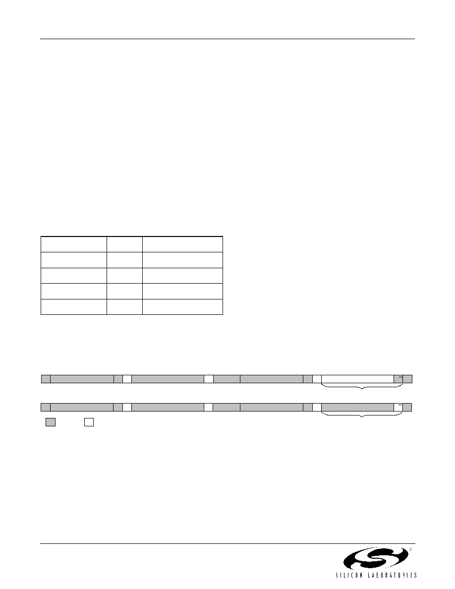
Si2107/08/09/10
30
Preliminary Rev. 0.7
7. I2C Control Interface
The I2C bus interface is provided for configuration and
monitoring of all internal registers. The Si2107/08/09/10
supports the 7-bit addressing procedure and is capable
of operating at rates up to 400 kbps. Individual data
transfers to and from the device are 8-bits. The I2C bus
consists of two wires: a serial clock line (SCL) and a
serial data line (SDA). The device always operates as a
bus slave. Read and write operations are performed in
accordance with the I2C-bus specification and the
following sequences.
The first byte after the START condition consists of the
slave address (SLAVE ADR, 7-bits) of the target device.
The slave address is configured during a hard reset by
setting the voltage on the ADDR pin. Possible slave
addresses and their corresponding ADDR voltages are
listed in Table 18.
Four addresses are available, allowing up to four
devices to share the same I2C bus. The R/W bit
determines the direction of data transfer. During a read
operation, data is sent from the device to the bus
master. During a write, data is sent from the bus master
to the device. The field labeled "DATA (ADR)" must
contain the 8-bit address of the target register. The data
to be transferred to or from the target register must be
placed in the following 8-bit "DATA" field. When the
auto-increment feature is enabled, INC_DS, the target
register address, is automatically incremented for
subsequent data transfers until a STOP condition ends
the operation.
Some registers in the device are larger than the 8-bit
DATA field permitted by I2C. These registers are split
into 8-bit addressable chunks that are uniquely
identified by a positional suffix. The suffix L indicates the
low-byte; the suffix M indicates the middle-byte (for 24-
bit registers only), and the suffix H indicates the high-
byte.
To read a multibyte register as a single unit, the low byte
must be read first. This forces the device to sample and
hold the contents of the remaining bytes until the
multibyte read is complete. If a STOP condition occurs
before the operation is complete, the buffered data is
discarded.
To write a multibyte register as a single unit, the low
byte must be written first. All bytes must be transferred
to the device before the multibyte value is recorded. If a
STOP condition occurs before the operation is
complete, the buffered data is discarded.
The slave address consists of a fixed part and a
programmable part. The voltage of the ADDR pin is
used to set the two least significant bits of the address
during device power-up according to the table below.
This enables up to four devices to share the same I2C
bus.
Figure 17. I2C Interface Protocol
Table 18. I2C Slave Address Selection
Fixed Address
LSBs
ADDR Voltage (V)
11010
00
V
3.3
(pullup)
11010
01
2/3 x V
3.3
±10%
11010
10
1/3 x V
3.3
±10%
11010
11
0 (pulldown)
Read Operation
W rite Operation
S
SLAVE ADR
W
A
DATA (ADR)
A
S
r
or P
SLAVE ADR
R
A
DATA
A/A P
S
SLAVE ADR
W
A
DATA (ADR)
A
S
r
or P
SLAVE ADR
W
A
DATA
A/A P
n bytes + ack
n bytes + ack
A = Acknowledge S = START condition
R = Read (1)
P = STOP condition
W= W rite (0)
S
r
= Repeated START condition
Master
Slave
Si2107/08/09/10
Preliminary Rev. 0.7
31
8. Control Registers
The control registers can be divided into three main classes: Initialization, Run-time, and Status. Initialization
registers ("I") need only be programmed once following device power-up. Run-time registers ("RT") are the primary
registers for device control. Status registers ("S") provide device state information. The corresponding category of
each register is indicated in the rightmost column of Table 19.
Table 19. Register Summary
Name
I2C
Addr.
D7
D6
D5
D4
D3
D2
D1
D0
System Configuration
Device ID
00h
DEV[3:0]
REV[3:0]
S
System Mode
01h
INC_DS
MOD[1:0]
SYSM[2:0]
I
TS Ctrl 1
02h
TSEP
TSVP
TSSP
TSSL
TSCM
TSCE
TSDF
TSM
I
TS Ctrl 2
03h
TSPCS
TSCD
TSDD
TSPG
TSSCR[1:0]
I
Pin Ctrl 1
04h
INT_EN
INTT
INTP
TSE_OE
TSV_OE
TSS_OE
TSC_OE
TSD_OE
I
Pin Ctrl 2
05h
GPO
PSEL[1:0]
I
Bypass
06h
DS_BP
RS_BP
DI_BP
I
Interrupts
Int En 1
07h
RCVL_E
AGCL_E
CEL_E
SRL_E
STL_E
CRL_E
VTL_E
FSL_E
I
Int En 2
08h
RCVU_E AGCTS_E
STU_E
CRU_E
VTU_E
FSU_E
AQF_E
I
Int En 3
09h
CN_E
VTBER_E
RSER_E MSGPE_E
FE_E
FF_E
MSGR_E
MSGTD_E
I
Int En 4
0Ah
SCD_E
OCD_E
I
Int Stat 1
0Bh
RCVL_I
AGCL_I
CEL_I
SRL_I
STL_I
CRL_I
VTL_I
FSL_I
S
Int Stat 2
0Ch
RCVU_I
AGCTS_I
STU_I
CRU_I
VTU_I
FSU_I
AQF_I
S
Int Stat 3
0Dh
CN_I
VTBR_I
RSER_I MSGPE_I
FE_I
FF_I
MSGR_I
MSGTO_I
S
Int Stat 4
0Eh
SCD_I
OCD_I
S
Receiver Status
Lock Stat 1
0Fh
AGCL
CEL
SRL
STL
CRL
VTL
FSL
S
Lock Stat 2
10h
RCVL
S
Acq Stat
11h
AQF
AGCF
CEF
SRF
STF
CRF
VTF
FSF
S
Tuning Control
Acq Ctrl 1
14h
AQS
RT
ADC SR
15h
ADCSR[7:0]
RT
Coarse Tune
16h
CTF[7:0]
RT

Si2107/08/09/10
32
Preliminary Rev. 0.7
Fine Tune L
17h
FTF[7:0]
RT
Fine Tune H
18h
FTF[14:8]
RT
CE Ctrl
29h
CESR[2:0]
I
CE Offset L
36h
CFO[7:0]
RT
CE Offset H
37h
CFO[15:8]
RT
CE Err L
38h
CFER[7:0]
RT
CE Err H
39h
CFER[15:8]
RT
SR Ctrl
3Ah
SRUK
RT
Sym Rate L
3Fh
SR[7:0]
RT
Sym Rate M
40h
SR[15:8]
RT
Sym Rate H
41h
SR[23:16]
RT
SR Max
42h
SRMX[7:0]
RT
SR Min
43h
SRMN[7:0]
RT
CN Ctrl
7Ch
CNS
CNM
CNW[1:0]
I
CN TH
7Dh
CNET[7:0]
I
CN L
7Eh
CNL[7:0]
RT
CN H
7Fh
CNL[15:8]
RT
Channel Decoder
VT Ctrl 1
A0h
VTCS[5:0]
I
VT Ctrl 2
A2h
VTERS
VTERM
VTERW[1:0]
RT
VT Stat
A3h
VTRS[2:0]
VTPS
VTIQS
S
VT BER Cnt L
ABh
VTBRC[7:0]
RT
VT BER Cnt H
ACh
VTBRC[15:8]
RT
RS Err Ctrl
B0h
RSERS
RSERM
RSERW
RSERT[1:0]
RT
RS Err Cnt L
B1h
RSERC[7:0]
RT
RS Err Cnt H
B2h
RSERC[15:8]
RT
DS Ctrl
B3h
DST_DS
DSO_DS
I
PRBS Ctl
B5h
PRBS_
START
PRBS_
INVERT
PRBS_
SYNC
PRBS_HEADER_SIZE
RT
Table 19. Register Summary (Continued)
Name
I2C
Addr.
D7
D6
D5
D4
D3
D2
D1
D0
Si2107/08/09/10
Preliminary Rev. 0.7
33
Automatic Gain Control
AGC Ctrl 1
23h
AGCW[1:0]
I
AGC Ctrl 2
24h
AGCTR[3:0]
AGCO[3:0]
I
AGC 1≠2 Gain
25h
AGC2[3:0]
AGC1[3:0]
I
AGC 3≠4 Gain
26h
AGC4[3:0]
AGC3[3:0]
I
AGC TH
27h
AGCTH[6:0]
I
AGC PL
28h
AGCPWR[6:0]
S
DAGC 1 Ctrl
75h
DAGC1_EN
DAGC1W[1:0]
DAGC1T DAGC1HOLD DAGC1HOST
I
DAGC1 L
76h
DAGC1[7:0]
I
DAGC1 H
77h
DAGC1[15:8]
I
DAGC2 Ctrl
78h
DAGC2[3:0]
DAGC2W[1:0]
DAGC2TDIS
I
DAGC2 TH
79h
DAGC2T[7:0]
I
DAGC2Lvl L
7Ah
DAGC2GA[7:0]
I
DAGC2Lvl H
7Bh
DAGC2GA[15:8]
I
LNB Supply Controller
LNB Ctrl 1
C0h
LNBS
LNBV
LNBCT
LNBB
MMSG
MSGL[2:0]
RT
LNB Ctrl 2
C1h
LNBM[1:0]
BRST_DS
TFS
RT
LNB Ctrl 3
C2h
TDIR
TT
TR
RT
LNB Ctrl 4
C3h
TFQ[7:0]
RT
LNB Stat
C4h
FE
FF
MSGPE
MSGR
MSGTO
MSGRL[2:0]
S
Msg FIFO 1
C5h
FIFO1[7:0]
RT
Msg FIFO 2
C6h
FIFO2[7:0]
RT
Msg FIFO 3
C7h
FIFO3[7:0]
RT
Msg FIFO 4
C8h
FIFO4[7:0]
RT
Msg FIFO 5
C9h
FIFO5[7:0]
RT
Msg FIFO 6
CAh
FIFO6[7:0]
RT
LNB S Ctrl1
CBh
VLOW[3:0]
VHIGH[3:0]
I
LNB S Ctrl2
CCh
ILIM[1:0]
IMAX[1:0]
SLOT[1:0]
OLOT[1:0]
I
LNB S Ctrl3
CDh
VMON[7:0]
S
Table 19. Register Summary (Continued)
Name
I2C
Addr.
D7
D6
D5
D4
D3
D2
D1
D0

Si2107/08/09/10
34
Preliminary Rev. 0.7
LNB S Ctrl4
CEh
LNBL
LNB_EN
COMP
LNBLVL
LNBMD
I
LNB S Stat
CFh
SCD
OCD
S
Table 19. Register Summary (Continued)
Name
I2C
Addr.
D7
D6
D5
D4
D3
D2
D1
D0

Si2107/08/09/10
Preliminary Rev. 0.7
35
Register 00h. Device ID Register
Bit
D7
D6
D5
D4
D3
D2
D1
D0
Name
DEV[3:0]
REV[3:0]
Bit
Name
Function
7:4
DEV[3:0]
Device ID.
0h = Si2110
1h = Si2109
2h = Si2108
3h = Si2107
3:0
REV[3:0]
Revision.
Current revision = 3h
Register 01h. System Mode
Bit
D7
D6
D5
D4
D3
D2
D1
D0
Name
0
0
INC_DS
MOD[1:0]
SYSM[2:0]
Bit
Name
Function
7:6
Reserved
Program to zero.
5
INC_DS
I2C Automatic Address Increment Disable.
0 = Enabled (default)
1 = Disabled
4:3
MOD[1:0]
Modulation Selection.
00 = BPSK Demodulation
01 = QPSK Demodulation (default)
10 = Reserved
11 = Reserved
2:0
SYSM[2:0]
System Mode.
000 = DVB-S (default)
001 = DSS
010≠111 = Reserved

Si2107/08/09/10
36
Preliminary Rev. 0.7
Register 02h. Transport Stream Control 1
Bit
D7
D6
D5
D4
D3
D2
D1
D0
Name
TSEP
TSVP
TSSP
TSSL
TSCM
TSCE
TSDF
TSM
Bit
Name
Function
7
TSEP
Transport Stream Error Polarity.
0 = Active high (default)
1 = Active low
6
TSVP
Transport Stream Valid Polarity.
0 = Active high (default)
1 = Active low
5
TSSP
Transport Stream Sync Polarity.
0 = Active high (default)
1 = Active low
4
TSSL
Transport Stream Start Length.
0 = Byte wide (default)
1 = Bit wide
Note: This bit is ignored in parallel mode.
3
TSCM
Transport Stream Clock Mode.
0 = Gapped mode (default)
1 = Continuous mode
2
TSCE
Transport Stream Clock Edge.
0 = Data transitions on rising edge (default)
1 = Data transitions on falling edge
1
TSDF
Transport Stream Serial Data Format.
0 = MSB first (default)
1 = LSB first
Note: This bit is ignored in parallel mode
0
TSM
Transport Stream Mode.
0 = Serial (default)
1 = Parallel

Si2107/08/09/10
Preliminary Rev. 0.7
37
Register 03h. Transport Stream Control 2
Bit
D7
D6
D5
D4
D3
D2
D1
D0
Name
0
TSPCS
TSCD
TSDD
TSPG
TSSCR[1:0]
Bit
Name
Function
7:6
Reserved
Program to zero.
5
TSPCS
Transport Stream Parallel Clock Smoother.
Smoothens TS_CLK to ~50% duty cycle.
0 = Smoothing disabled
1 = Smoothen clock to ~50% duty cycle (default)
4
TSCD
Transport Stream Clock Delay.
Adds delay to TS_CLK to adjust clock-data timing relationship.
0 = Normal operation (default)
1 = Delay clock relative to data
3
TSDD
Transport Stream Data Delay.
Adds delay to TS_DATA, TS_SYNC, TS_VAL, TS_ERR output to adjust
clock-data timing relationship.
0 = Normal operation (default)
1 = Delay data relative to clock
2
TSPG
Transport Stream Parity Gate.
0 = Normal operation (default)
1 = Zero data lines during parity
1:0
TSSCR[1:0]
Transport Stream Serial Clock Rate.
00 = 80≠88.5 MHz (default)
01 = 76.8≠82.8 MHz
10 = 54.9≠59.2 MHz
11 = 35≠37.7 MHz

Si2107/08/09/10
38
Preliminary Rev. 0.7
Register 04h. Pin Control 1
Bit
D7
D6
D5
D4
D3
D2
D1
D0
Name
INT_EN
INTT
INTP
TSE_OE
TSV_OE
TSS_OE
TSC_OE
TSD_OE
Bit
Name
Function
7
INT_EN
Interrupt Pin Enable.
0 = Disabled (default)
1 = Enabled
6
INTT
Interrupt Pin Type.
0 = CMOS (default)
1 = Open drain/source
5
INTP
Interrupt Polarity.
0 = Active low (default)
1 = Active high
4
TSE_OE
Transport Stream Error Output Enable.
0 = Enabled
1 = Tri-state (default)
3
TSV_OE
Transport Stream Valid Output Enable.
0 = Enabled
1 = Tri-state (default)
2
TSS_OE
Transport Stream Sync Output Enable.
0 = Enabled
1 = Tri-state (default)
1
TSC_OE
Transport Stream Clock Output Enable.
0 = Enabled
1 = Tri-state (default)
0
TSD_OE
Transport Stream Data Output Enable.
0 = Enabled
1 = Tri-state (default)

Si2107/08/09/10
Preliminary Rev. 0.7
39
Register 05h. Pin Control 2
Bit
D7
D6
D5
D4
D3
D2
D1
D0
Name
0
0
1
0
0
GPO
PSEL[1:0]
Bit
Name
Function
7:3
Reserved
Program to zero (except bit D5, which is programmed to 1).
2
GPO
General Purpose Output Control.
Controls output of pin 30 when PSEL = 10
0 = Output logic zero. (default)
1 = Output logic 1.
1:0
PSEL[1:0]
Pin Select (Pin 30).
00 = Interrupt (default)
01 = Receiver lock indicator
10 = General Purpose Output
11 = Reserved
Register 06h. Bypass
Bit
D7
D6
D5
D4
D3
D2
D1
D0
Name
0
0
DS_BP
RS_BP
DI_BP
0
0
0
Bit
Name
Function
7:6
Reserved
Program to zero.
5
DS_BP
Descrambler Bypass.
0 = Normal operation (default)
1 = Bypass
Note: This bit is ignored in DSS mode; the descrambler is automatically
bypassed.
4
RS_BP
Reed-Solomon Bypass.
0 = Normal operation (default)
1 = Bypass
3
DI_BP
Deinterleaver Bypass.
0 = Normal operation (default)
1 = Bypass
2:0
Reserved
Program to zero.

Si2107/08/09/10
40
Preliminary Rev. 0.7
Register 07h. Interrupt Enable 1
Bit
D7
D6
D5
D4
D3
D2
D1
D1
Name
RCVL_E
AGCL_E
CEL_E
SRL_E
STL_E
CRL_E
VTL_E
FSL_E
Bit
Name
Function
7
RCVL_E
Receiver Lock Interrupt Enable.
0 = Disabled (default)
1 = Enabled
6
AGCL_E
AGC Lock Interrupt Enable.
0 = Disabled (default)
1 = Enabled
5
CEL_E
Carrier Estimator Lock Interrupt Enable.
0 = Disabled (default)
1 = Enabled
4
SRL_E
Symbol Rate Lock Interrupt Enable.
0 = Disabled (default)
1 = Enabled
Note: Available on Si2109/10 only.
3
STL_E
Symbol Timing Lock Interrupt Enable.
0 = Disabled (default)
1 = Enabled
2
CRL_E
Carrier Recovery Lock Interrupt Enable.
0 = Disabled (default)
1 = Enabled
1
VTL_E
Viterbi Search Lock Interrupt Enable.
0 = Disabled (default)
1 = Enabled
0
FSL_E
Frame Sync Lock Interrupt Enable.
0 = Disabled (default)
1 = Enabled

Si2107/08/09/10
Preliminary Rev. 0.7
41
Register 08h. Interrupt Enable 2
Bit
D7
D6
D5
D4
D3
D2
D1
D1
Name
RCVU_E
AGCTS_E
STU_E
CRU_E
VTU_E
FSU_E
0
AQF_E
Bit
Name
Function
7
RCVU_E
Receiver Unlock Interrupt Enable.
0 = Disabled (default)
1 = Enabled
6
AGCTS_E
AGC Tracking Threshold Interrupt Enable.
0 = Disabled (default)
1 = Enabled
5
STU_E
Symbol Timing Unlock Interrupt Enable.
0 = Disabled (default)
1 = Enabled
4
CRU_E
Carrier Recovery Unlock Interrupt Enable.
0 = Disabled (default)
1 = Enabled
3
VTU_E
Viterbi Search Unlock Interrupt Enable.
0 = Disabled (default)
1 = Enabled
2
FSU_E
Frame Sync Unlock Interrupt Enable.
0 = Disabled (default)
1 = Enabled
1
Reserved
Program to zero.
0
AQF_E
Acquisition Fail Interrupt Enable.
0 = Disabled (default)
1 = Enabled

Si2107/08/09/10
42
Preliminary Rev. 0.7
Register 09h. Interrupt Enable 3
Bit
D7
D6
D5
D4
D3
D2
D1
D1
Name
CN_E
VTBER_E
RSER_E
MSGPE_E
FE_E
FF_E
MSGR_E
MSGTD_E
Bit
Name
Function
7
CN_E
C/N Estimator Interrupt Enable.
0 = Disabled (default)
1 = Enabled
6
VTBER_E
Viterbi BER Interrupt Enable.
0 = Disabled (default)
1 = Enabled
5
RSER_E
Reed-Solomon Error Measurement Interrupt Enable.
0 = Disabled (default)
1 = Enabled
4
MSGPE_E
LNB Message Parity Error Interrupt Enable.
0 = Disabled (default)
1 = Enabled
3
FE_E
LNB Transmit FIFO Empty Interrupt Enable.
0 = Disabled (default)
1 = Enabled
2
FF_E
LNB Receive FIFO Full Interrupt Enable.
0 = Disabled (default)
1 = Enabled
1
MSGR_E
LNB Receive Message Interrupt Enable.
0 = Disabled (default)
1 = Enabled
0
MSGTD_E
LNB Receive Timeout Interrupt Enable.
0 = Disabled (default)
1 = Enabled

Si2107/08/09/10
Preliminary Rev. 0.7
43
Register 0Ah. Interrupt Enable 4
Bit
D7
D6
D5
D4
D3
D2
D1
D0
Name
0
0
0
0
0
0
SCD_E
OCD_E
Bit
Name
Function
7:2
Reserved
Program to zero.
1
SCD_E
Short Circuit Detect Interrupt Enable.
0 = Disabled (default)
1 = Enabled
0
OCD_E
Over Current Detect Interrupt Enable.
0 = Disabled (default)
1 = Enabled

Si2107/08/09/10
44
Preliminary Rev. 0.7
Register 0Bh. Interrupt Status 1
Bit
D7
D6
D5
D4
D3
D2
D1
D1
Name
RCVL_I
AGCL_I
CEL_I
SRL_I
STL_I
CRL_I
VTL_I
FSL_I
Bit
Name
Function
7
RCVL_I
Receiver Lock Interrupt.
0 = Disabled (default)
1 = Enabled
6
AGCL_I
AGC Lock Interrupt.
0 = Disabled (default)
1 = Enabled
5
CEL_I
Carrier Estimator Lock Interrupt.
0 = Disabled (default)
1 = Enabled
4
SRL_I
Symbol Rate Lock Interrupt.
0 = Disabled (default)
1 = Enabled
Note: Available on Si2109/10 only.
3
STL_I
Symbol Timing Lock Interrupt.
0 = Disabled (default)
1 = Enabled
2
CRL_I
Carrier Recovery Lock Interrupt.
0 = Disabled (default)
1 = Enabled
1
VTL_I
Viterbi Search Lock Interrupt.
0 = Disabled (default)
1 = Enabled
0
FSL_I
Frame Sync Lock Interrupt.
0 = Disabled (default)
1 = Enabled

Si2107/08/09/10
Preliminary Rev. 0.7
45
Register 0Ch. Interrupt Status 2
Bit
D7
D6
D5
D4
D3
D2
D1
D1
Name
RCVU_I
AGCTS_I
STU_I
CRU_I
VTU_I
FSU_I
0
AQF_I
Bit
Name
Function
7
RCVU_I
Receiver Unlock Interrupt.
6
AGCTS_I
AGC Tracking Threshold Interrupt.
0 = Normal operation (default)
1 = Event recorded
5
STU_I
Symbol Timing Unlock Interrupt.
0 = Normal operation (default)
1 = Event recorded
4
CRU_I
Carrier Recovery Unlock Interrupt.
0 = Normal operation (default)
1 = Event recorded
3
VTU_I
Viterbi Search Unlock Interrupt.
0 = Normal operation (default)
1 = Event recorded
2
FSU_I
Frame Sync Unlock Interrupt.
0 = Normal operation (default)
1 = Event recorded
1
Reserved
Program to zero.
0
AQF_I
Acquisition Fail Interrupt.
0 = Normal operation (default)
1 = Event recorded

Si2107/08/09/10
46
Preliminary Rev. 0.7
Register 0Dh. Interrupt Status 3
Bit
D7
D6
D5
D4
D3
D2
D1
D1
Name
CN_I
VTBR_I
RSER_I
MSGPE_I
FE_I
FF_I
MSGR_I
MSGTO_I
Bit
Name
Function
7
CN_I
C/N Estimator Interrupt.
0 = Normal operation (default)
1 = Event recorded
6
VTBR_I
Viterbi BER Interrupt.
0 = Normal operation (default)
1 = Event recorded
5
RSER_I
Reed-Solomon Error Measurement Complete Interrupt.
0 = Normal operation (default)
1 = Event recorded
4
MSGPE_I
LNB Message Parity Error Interrupt.
0 = Normal operation (default)
1 = Event recorded
3
FE_I
LNB Transmit FIFO Empty Interrupt.
0 = Normal operation (default)
1 = Event recorded
2
FF_I
LNB Receive FIFO Full Interrupt.
0 = Normal operation (default)
1 = Event recorded
1
MSGR_I
LNB Receive Message Interrupt.
0 = Normal operation (default)
1 = Event recorded
0
MSGTO_I
LNB Receive Timeout Interrupt.
0 = Normal operation (default)
1 = Event recorded

Si2107/08/09/10
Preliminary Rev. 0.7
47
Register 0Eh. Interrupt Status 4
Bit
D7
D6
D5
D4
D3
D2
D1
D0
Name
0
0
0
0
0
0
SCD_I
OCD_I
Bit
Name
Function
7:2
Reserved
Program to zero.
1
SCD_I
Short Circuit Detect Interrupt.
0 = Normal operation (default)
1 = Event recorded
0
OCD_I
Over Current Detect Interrupt.
0 = Normal operation (default)
1 = Event recorded

Si2107/08/09/10
48
Preliminary Rev. 0.7
Register 0Fh. Lock Status 1
Bit
D7
D6
D5
D4
D3
D2
D1
D0
Name
0
AGCL
CEL
SRL
STL
CRL
VTL
FSL
Bit
Name
Function
7
Reserved
Program to zero.
6
AGCL
AGC Lock Status.
0 = Pending (default)
1 = Complete
5
CEL
Carrier Estimation Status.
0 = Pending (default)
1 = Complete
4
SRL
Symbol Rate Estimation Status.
0 = Pending (default)
1 = Complete
Note: Available on Si2109/10 only.
3
STL
Symbol Timing Lock Status.
0 = Unlocked (default)
1 = Locked
2
CRL
Carrier Lock Status.
0 = Unlocked (default)
1 = Locked
1
VTL
Viterbi Lock Status.
0 = Unlocked (default)
1 = Locked
0
FSL
Frame Sync Lock Status.
0 = Unlocked (default)
1 = Locked
Register 10h. Lock Status 2
Bit
D7
D6
D5
D4
D3
D2
D1
D0
Name
RCVL
0
0
0
0
0
0
0
Bit
Name
Function
7
RCVL
Receiver Lock Status.
0 = Unlocked (default)
1 = Locked
6:0
Reserved
Program to zero.

Si2107/08/09/10
Preliminary Rev. 0.7
49
Register 11h. Acquisition Status
Bit
D7
D6
D5
D4
D3
D2
D1
D1
Name
AQF
AGCF
CEF
SRF
STF
CRF
VTF
FSF
Bit
Name
Function
7
AQF
Receiver Acquisition Status.
0 = Normal operation (default)
1 = Acquisition failed
6
AGCF
AGC Search Status.
0 = Normal operation (default)
1 = Gain control limit reached
5
CEF
Carrier Estimation Search Status.
0 = Normal operation (default)
1 = Carrier offset not found
4
SRF
Symbol Rate Search Status.
0 = Normal operation (default)
1 = Search failed
Note: Available on Si2109/10 only.
3
STF
Symbol Timing Search Status.
0 = Normal operation (default)
1 = Search failed
2
CRF
Carrier Search Status.
0 = Normal operation (default)
1 = Search failed
1
VTF
Viterbi Search Status.
0 = Normal operation (default)
1 = Search failed
0
FSF
Frame Sync Search Status.
0 = Normal operation (default)
1 = Search failed
Si2107/08/09/10
50
Preliminary Rev. 0.7
Register 14h. Acquisition Control 1
Bit
D7
D6
D5
D4
D3
D2
D1
D0
Name
AQS
0
0
0
0
0
0
0
Bit
Name
Function
7
AQS
Automatic Acquisition Start.
Writing a one to this bit initiates the acquisition sequence. This bit is
automatically cleared when the acquisition sequence completes.
6:0
Reserved
Program to zero.
Register 15h. ADC Sampling Rate
Bit
D7
D6
D5
D4
D3
D2
D1
D0
Name
ADCSR[7:0]
Bit
Name
Function
7:0
ADCSR[7:0]
ADC Sampling Rate.
f
s
= ADCSR x 1 MHz
Default: C8h (200 MHz)
Register 16h. Coarse Tune Frequency
Bit
D7
D6
D5
D4
D3
D2
D1
D0
Name
CTF[7:0]
Bit
Name
Function
7:0
CTF[7:0]
Coarse Tune Frequency.
Calculation of the coarse tune value is determined by the reference
software driver.
f
coarse
= CTF x 10 MHz
Default: 00h

Si2107/08/09/10
Preliminary Rev. 0.7
51
Register 17h. Fine Tune Frequency L
Bit
D7
D6
D5
D4
D3
D2
D1
D0
Name
FTF[7:0]
Bit
Name
Function
7:0
FTF[7:0]
Fine Tune Frequency (Low Byte).
where FTF is stored as a 2s complement value.
Calculation of the fine tune value is determined by the reference soft-
ware driver.
Default: 00h
Register 18h. Fine Tune Frequency H
Bit
D7
D6
D5
D4
D3
D2
D1
D0
Name
0
FTF[14:8]
Bit
Name
Function
7
Reserved
Program to zero.
6:0
FTF[14:8]
Fine Tune Frequency (High Byte).
See Register 17h.
Register 23h. Analog AGC Control 1
Bit
D7
D6
D5
D4
D3
D2
D1
D0
Name
0
0
AGCW[1:0]
0
0
0
0
Bit
Name
Function
7:6
Reserved
Program to zero.
5:4
AGCW[1:0]
AGC Measurement Window.
Acquisition
Tracking
00 = 1024 (default)
65536 samples (default)
01 = 2048
131072 samples
10 = 4096
262144 samples
11 = 8192
524288 samples
3:0
Reserved
Program to zero.
f
fine
FTF
f
s
2
14
--------
◊
=
Si2107/08/09/10
52
Preliminary Rev. 0.7
Register 24h. AGC Control 2
Bit
D7
D6
D5
D4
D3
D2
D1
D0
Name
AGCTR[3:0]
AGCO[3:0]
Bit
Name
Function
7:4
AGCTR[3:0]
AGC Tracking Threshold.
Specifies the maximum difference between AGCPWR (28h) and
AGCTH (27h) before making a gain adjustment.
Default: 1000.
3:0
AGCO[3:0]
AGC Gain Offset.
Applies a static gain offset to the input channel.
0000 = +0 dB (default)
0001 = +1 dB
...
1110 = +14 dB
1111 = +15 dB
Register 25h. Analog AGC 1≠2 Gain
Bit
D7
D6
D5
D4
D3
D2
D1
D0
Name
AGC2[3:0]
AGC1[3:0]
Bit
Name
Function
7:4
AGC2[3:0]
Analog Gain stage 2 setting.
Default: 0h
3:0
AGC1[3:0]
Analog Gain stage 1 setting.
Default: 0h
Register 26h. Analog AGC 3≠4 Gain
Bit
D7
D6
D5
D4
D3
D2
D1
D0
Name
AGC4[3:0]
AGC3[3:0]
Bit
Name
Function
7:4
AGC4[3:0]
Analog Gain stage 4 setting
Default: 0h
3:0
AGC3[3:0]
Analog Gain stage 3 setting
Default: 0h
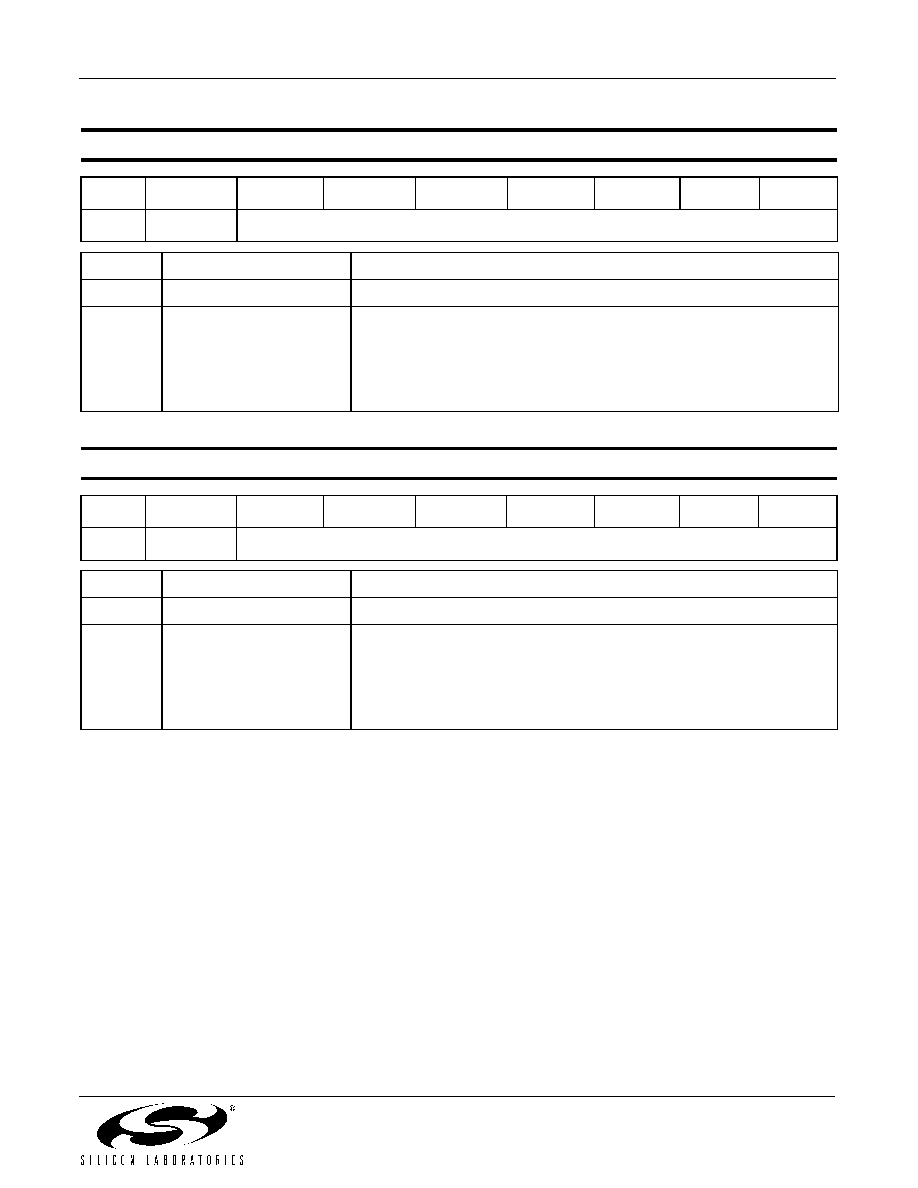
Si2107/08/09/10
Preliminary Rev. 0.7
53
Register 27h. AGC Threshold
Bit
D7
D6
D5
D4
D3
D2
D1
D0
Name
0
AGCTH[6:0]
Bit
Name
Function
7
Reserved
Program to zero.
6:0
AGCTH[6:0]
AGC Threshold.
The value specified in this register corresponds to the desired AGC
power level. The AGC loop adjusts the gain of the system to drive the
AGC power level to this value.
Default: 20h.
Register 28h. AGC Power Level
Bit
D7
D6
D5
D4
D3
D2
D1
D0
Name
0
AGCPWR[6:0]
Bit
Name
Function
7
Reserved
Program to zero.
6:0
AGCPWR[6:0]
AGC Power Level.
Represents the measured input power level after the ADC in rms format.
The measurement window is set by AGCW (23h[6:4]). This register sat-
urates at full scale.
Default: 00h.

Si2107/08/09/10
54
Preliminary Rev. 0.7
Register 29h. Carrier Estimation Control
Bit
D7
D6
D5
D4
D3
D2
D1
D0
Name
0
0
0
0
1
CESR[2:0]
Bit
Name
Function
7:4
Reserved
Program to zero.
3
Reserved
Program to one.
2:0
CESR[2:0]
Carrier Estimation Search Range.
000 = Reserved
001 = ± f
s
/ 32
(± 6.3 MHz typ.) (default)
010 = ± f
s
/ 64
(± 3.1 MHz typ.)
011 = ± f
s
/ 128
(± 1.6 MHz typ.)
100 = ± f
s
/ 256
(± 0.8 MHz typ.)
101 = ± f
s
/ 512
(± 0.4 MHz typ.)
110 = ± f
s
/ 1024
(± 0.2 MHz typ.)
111 = ± f
s
/ 2048
(± 0.1 MHz typ.)
Register 36h. Carrier Estimator Offset L
Bit
D7
D6
D5
D4
D3
D2
D1
D0
Name
CFO[7:0]
Bit
Name
Function
7:0
CFO[7:0]
Carrier Frequency Offset (Low Byte).
Designed to store a residual carrier frequency offset for future acquisi-
tions. Used during carrier offset estimation to adjust the center fre-
quency.
Note: CFO is a 16-bit Twos complement number.
Default: 00h
Search center frequency
f
desired
CFO
+
f
s
2
15
--------
◊
Hz
=

Si2107/08/09/10
Preliminary Rev. 0.7
55
Register 37h. Carrier Estimator Offset H
Bit
D7
D6
D5
D4
D3
D2
D1
D0
Name
CFO[15:8]
Bit
Name
Function
7:0
CFO[15:8]
Carrier Frequency Offset (High Byte).
See register 36h.
Register 38h. Carrier Frequency Offset Error L
Bit
D7
D6
D5
D4
D3
D2
D1
D0
Name
CFER[7:0]
Bit
Name
Function
7:0
CFER[7:0]
Carrier Frequency Offset Error (Low Byte).
Stores the carrier frequency offset that is identified during the carrier
offset estimation stage.
Note: CFER is a 16-bit Twos complement number.
Default: 00h
Register 39h. Carrier Frequency Offset Error H
Bit
D7
D6
D5
D4
D3
D2
D1
D0
Name
CFER[15:8]
Bit
Name
Function
7:0
CFER[15:8]
Carrier Frequency Offset Error (High Byte).
See register 38h.
Offset
CFER
f
s
2
15
-------- Hz
◊
≠
=

Si2107/08/09/10
56
Preliminary Rev. 0.7
Register 3Ah. Symbol Rate Control (Si2109 and Si2110 only)
Bit
D7
D6
D5
D4
D3
D2
D1
D0
Name
0
SRUK
0
0
0
0
0
0
Bit
Name
Function
7
Reserved
Program to zero.
6
SRUK
Symbol Rate Unknown.
0 = Symbol rate is known. (default)
1 = Symbol rate is unknown.
5:0
Reserved
Program to zero.
Register 3Fh. Symbol Rate L
Bit
D7
D6
D5
D4
D3
D2
D1
D0
Name
SR[7:0]
Bit
Name
Function
7:0
SR[7:0]
Symbol Rate (Low Byte).
Default: 00h.
Register 40h. Symbol Rate M
Bit
D7
D6
D5
D4
D3
D2
D1
D0
Name
SR[15:8]
Bit
Name
Function
7:0
SR[15:8]
Symbol Rate (Mid Byte).
See register 3Fh.
Symbol rate
SR
f
s
2
24
--------
◊
Hz
=
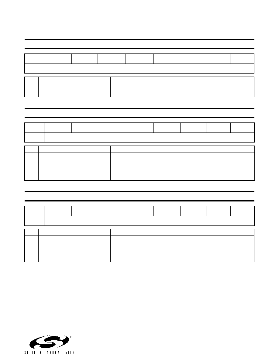
Si2107/08/09/10
Preliminary Rev. 0.7
57
Register 41h. Symbol Rate H
Bit
D7
D6
D5
D4
D3
D2
D1
D0
Name
SR[23:16]
Bit
Name
Function
7:0
SR[23:16]
Symbol Rate (High Byte).
See register 3F.
Register 42h. Symbol Rate Maximum (Si2109 and Si2110 only)
Bit
D7
D6
D5
D4
D3
D2
D1
D0
Name
SRMX[7:0]
Bit
Name
Function
7:0
SRMX[7:0]
Symbol Rate Estimation Maximum.
Default: 00h.
Register 43h. Symbol Rate Minimum (Si2109 and Si2110 only)
Bit
D7
D6
D5
D4
D3
D2
D1
D0
Name
SRMN[7:0]
Bit
Name
Function
7:0
SRMN[7:0]
Symbol Rate Estimation Minimum.
Default: 00h.
Max symbol rate
SRMX
f
s
2
16
--------
◊
Hz
=
Min symbol rate
SRMN
f
s
2
16
--------
◊
Hz
=

Si2107/08/09/10
58
Preliminary Rev. 0.7
Register 75h. Digital AGC 1 Control
Bit
D7
D6
D5
D4
D3
D2
D1
D0
Name
0
DAGC1_EN
DAGC1W[1:0]
DAGC1T
DAGC1HOLD
DAGC1HOST
0
Bit
Name
Function
7
Reserved
Program to 0 (device may change the value of this bit during opera-
tion)
6
DAGC1_EN
Enable digital AGC 1
0 = Disabled
1 = Enabled (default)
5:4
DAGC1W[1:0]
Digital AGC Measurement Window
00 = 256 samples
01 = 512 samples
10 = 1024 samples (default)
11 = 2048 samples
3
DAGC1T
Select AGC threshold
0 = ≠15 dBFS (default)
1 = ≠9 dBFS
2
DAGC1HOLD
Hold previous computed gain value on DAGC1
0 = Update gain after each calculation (default)
1 = Do not update gain value
1
DAGC1HOST
Host-controlled DAGC1
0 = Gain is determined by DAGC1 module. Digital AGC1 gain regis-
ter is read-only. (Default)
1 = Gain is determined by host and specified in Digital AGC1 Gain
Register (76h & 77h).
0
Reserved
Program to 0.
Register 76h. Digital AGC 1 Gain L
Bit
D7
D6
D5
D4
D3
D2
D1
D0
Name
DAGC1[7:0]
Bit
Name
Function
7:0
DAGC1[7:0]
Gain of digital AGC 1 (low-byte).
Default: 00h
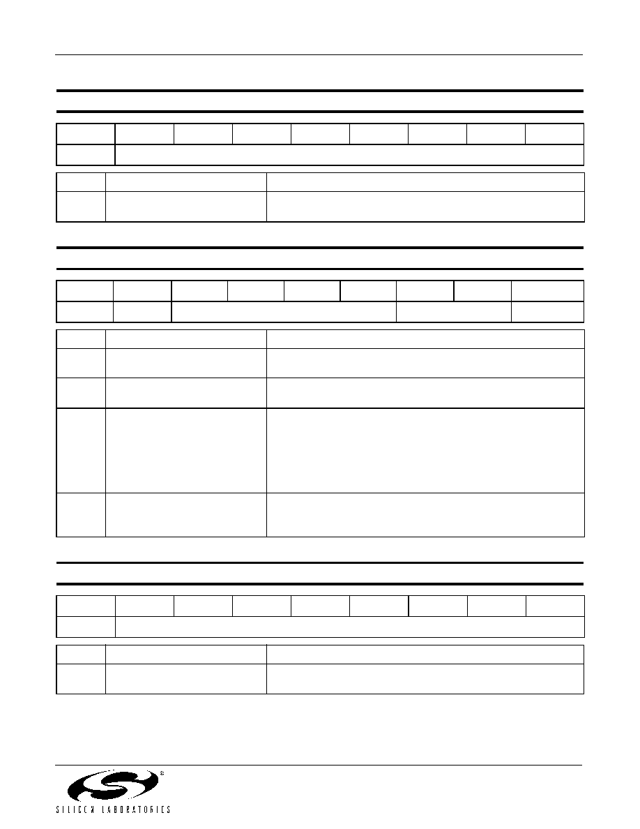
Si2107/08/09/10
Preliminary Rev. 0.7
59
Register 77h. Digital AGC 1 Gain H
Bit
D7
D6
D5
D4
D3
D2
D1
D0
Name
DAGC1[15:8]
Bit
Name
Function
7:0
DAGC1[15:8]
Gain of digital AGC 1 (high-byte).
Default: 00h
Register 78h. Digital AGC 2 Control
Bit
D7
D6
D5
D4
D3
D2
D1
D0
Name
Reserved
DAGC2[3:0]
DAGC2W[1:0]
DAGC2TDIS
Bit
Name
Function
7
Reserved
Program to 0 (device may change the value of this bit during opera-
tion)
6:3
DAGC2[3:0]
Digital AGC2 gain factor
Default: 0h
2:1
DAGC2W[1:0]
Digital AGC2 Measurement window
Acquisition Tracking
00 = 16 samples (default) 1024 samples (default)
01 = 32 samples
2048 samples
10 = 64 samples
4096 samples
11 = 128 samples
8192 samples
0
DAGC2TDIS
Digital AGC2 Automatic Tracking Disable
1 = Disable automatic tracking. Freeze applied to gain.
0 = Enable automatic tracking. (default)
Register 79h. Digital AGC 2 Threshold
Bit
D7
D6
D5
D4
D3
D2
D1
D0
Name
DAGC2T[7:0]
Bit
Name
Function
7:0
DAGC2T[7:0]
Digital AGC2 Threshold
Default: B5h

Si2107/08/09/10
60
Preliminary Rev. 0.7
Register 7Ah. Digital AGC 2 Level L
Bit
D7
D6
D5
D4
D3
D2
D1
D0
Name
DAGC2GA[7:0]
Bit
Name
Function
7:0
DAGC2GA[7:0]
Digital AGC2 Gain Auto (low byte).
Digital AGC2 gain applied to meet threshold
Default: 00h
Register 7Bh. Digital AGC 2 Level H
Bit
D7
D6
D5
D4
D3
D2
D1
D0
Name
DAGC2GA[15:8]
Bit
Name
Function
7:0
DAGC2GA[15:8]
Digital AGC2 Gain Auto (high byte).
See register 7Ah.
Default: 00h
Register 7Ch. C/N Estimator Control
Bit
D7
D6
D5
D4
D3
D2
D1
D0
Name
CNS
0
0
0
0
CNM
CNW[1:0]
Bit
Name
Function
7
CNS
C/N Estimator Start.
Writing a one to this bit initiates an C/N estimator and clears the result
stored in CNE_LEVEL. This bit is automatically cleared to zero when the
measurement period elapses.
6:3
Reserved
Program to zero.
2
CNM
C/N Estimator Mode.
0 = Finite window
1 = Infinite window (default)
1:0
CNW[1:0]
C/N Measurement Window.
00 = 1024 samples
01 = 4096 samples (default)
10 = 16384 samples
11 = 65536 samples
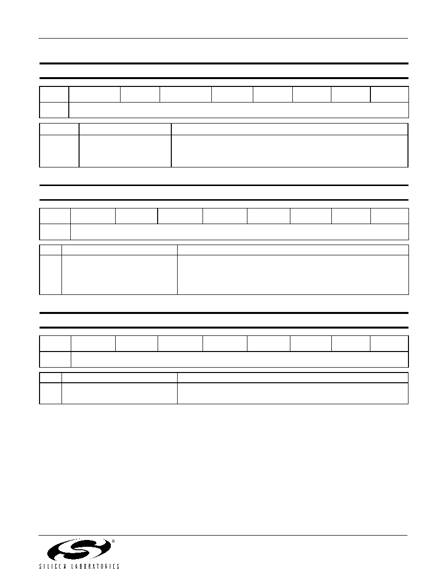
Si2107/08/09/10
Preliminary Rev. 0.7
61
Register 7Dh. C/N Estimator Threshold0
Bit
D7
D6
D5
D4
D3
D2
D1
D0
Name
CNET[7:0]
Bit
Name
Function
7:0
CNET[7:0]
C/N Estimator Threshold.
This value defines a noise threshold for the C/N estimator.
Default 13h.
Register 7Eh. C/N Estimator Level L
Bit
D7
D6
D5
D4
D3
D2
D1
D0
Name
CNL[7:0]
Bit
Name
Function
7:0
CNL[7:0]
C/N Estimator Level (Low Byte).
The value in this register is to be used with an external lookup table to
estimate the C/N of the input signal.
Default: 00h.
Register 7Fh. C/N Estimator Level H
Bit
D7
D6
D5
D4
D3
D2
D1
D0
Name
CNL[15:8]
Bit
Name
Function
7:0
CNL[15:8]
C/N Estimator Level (High Byte).
See Register 7Eh.

Si2107/08/09/10
62
Preliminary Rev. 0.7
Register A0h. Viterbi Search Control 1
Bit
D7
D6
D5
D4
D3
D2
D1
D0
Name
0
0
VTCS[5:0]
Bit
Name
Function
7:6
Reserved
Program to zero.
5:0
VTCS[5:0]
Viterbi Code Rate Search Parameter Enable.
The code rates to be used in the Viterbi search are selected by writing a
one into the appropriate bit position. The list below illustrates the rela-
tionship between bit position and code rate.
Bit 5 = 7/8 code rate (MSB)
Bit 4 = 6/7 code rate
Bit 3 = 5/6 code rate
Bit 2 = 3/4 code rate
Bit 1 = 2/3 code rate
Bit 0 = 1/2 code rate (LSB)
Default: All code rates selected (3Fh).
Register A2h. Viterbi Search Control 2
Bit
D7
D6
D5
D4
D3
D2
D1
D0
Name
Reserved
VTERS
VTERM
VTERW[1:0]
Bit
Name
Function
3
VTERS
Viterbi BER Measurement Start
Writing a 1 to this bit initiates the Viterbi BER measurement.
2
VTERM
Viterbi BER Measurement Mode
0 = finite window (default)
1 = infinite window
1:0
VTERW[1:0]
Viterbi BER Measurement Window
00 = 2
13
bits (default)
01 = 2
17
bits
10 = 2
21
bits
11 = 2
25
bits

Si2107/08/09/10
Preliminary Rev. 0.7
63
Register A3h. Viterbi Search Status
Bit
D7
D6
D5
D4
D3
D2
D1
D0
Name
VTRS[2:0]
Reserved
VTPS
VTIQS
Bit
Name
Function
7:5
VTRS[2:0]
Viterbi Current Code Rate Indicator.
000 = 1/2 code rate (default)
001 = 2/3 code rate
010 = 3/4 code rate
011 = 5/6 code rate
100 = 6/7 code rate
101 = 7/8 code rate
11x = Undefined
4:2
Reserved
Program to 0.
1
VTPS
Viterbi Constellation Rotation Phase Status.
0 = Not rotated (default)
1 = Rotated by 90 degrees
0
VTIQS
Viterbi I/Q Swap Status.
0 = Not swapped (default)
1 = Swapped
Register ABh. Viterbi BER Count L
Bit
D7
D6
D5
D4
D3
D2
D1
D0
Name
VTBRC[7:0]
Bit
Name
Function
7:0
VTBRC[7:0]
Viterbi BER Counter (Low Byte).
Stores the number of the Viterbi bit errors detected within the specified
measurement window. This register saturates when it reaches the limit
of its range.
Default: 00h
Si2107/08/09/10
64
Preliminary Rev. 0.7
Register ACh. Viterbi BER Count H
Bit
D7
D6
D5
D4
D3
D2
D1
D0
Name
VTBRC[15:8]
Bit
Name
Function
7:0
VTBRC[15:8]
Viterbi BER Counter (High Byte).
See Register ABh.
Register B0h. Reed-Solomon BER Error Monitor Control
Bit
D7
D6
D5
D4
D3
D2
D1
D0
Name
Reserved
RSERS
RSERM
RSERW
RSERT[1:0]
Bit
Name
Function
7:5
Reserved
Program to zero.
4
RSERS
Reed-Solomon BER Measurement Start.
Writing a 1 to this bit initiates the Reed-Solomon BER measurement.
3
RSERM
Reed-Solomon Measurement Mode.
0 = Finite window (default)
1 = Infinite window
2
RSERW
Reed-Solomon Measurement Window.
0 = 2
12
frames (default)
1 = 2
16
frames
1:0
RSERT[1:0]
Reed-Solomon Error Type.
00 = Corrected bit errors (default)
01 = Corrected byte errors
10 = Uncorrected packets
11 = PRBS errors
Si2107/08/09/10
Preliminary Rev. 0.7
65
Register B1h. Reed-Solomon Error Monitor Count L
Bit
D7
D6
D5
D4
D3
D2
D1
D0
Name
RSERC[7:0]
Bit
Name
Function
7:0
RSERC[7:0]
Reed-Solomon Error Counter (Low Byte).
Stores the number of RS or PRBS errors detected within the specified
window. This register saturates when it reaches the limit of its range.
Default: 00h
Register B2h. Reed-Solomon Error Monitor Count H
Bit
D7
D6
D5
D4
D3
D2
D1
D0
Name
RSERC[15:8]
Bit
Name
Function
7:0
RSERC[15:8]
Reed-Solomon Error Counter (High Byte).
See Register B1h.
Register B3h. Descrambler Control
Bit
D7
D6
D5
D4
D3
D2
D1
D0
Name
0
0
0
0
0
0
DST_DS
DSO_DS
Bit
Name
Function
7:2
Reserved
Program to zero.
1
DST_DS
Descrambler Transport Error Insertion Disable.
0 = Enabled (default)
1 = Disabled
0
DSO_DS
Descrambler Inverted SYNC Overwrite Disable.
0 = Enabled (default)
1 = Disabled

Si2107/08/09/10
66
Preliminary Rev. 0.7
Register B5h. PRBS Control
Bit
D7
D6
D5
D4
D3
D2
D1
D0
Name
PRBS_START PRBS_INVERT PRBS_SYNC
0
0
0
PRBS_HEADER_SIZE
Bit
Name
Function
7
PRBS_START
Start PRBS synchronization.
1 = Start PRBS synchronization
Default = 0
6
PRBS_INVERT
Invert PRBS output.
1 = PRBS inverted.
Default = 0
5
PRBS_SYNC
Synchronization achieved for PRBS test.
0 = Not synchronized.
1 = Synchronized
Default = 0
4:2
Reserved
Read returns zero.
1:0
PRBS_HEADER_SIZE
Packet header size (DVB-S/DSS)
00 = 1/0 (Default)
01 = 2/1
10 = 3/2
11 = 4/3

Si2107/08/09/10
Preliminary Rev. 0.7
67
Register C0h. LNB Control 1
Bit
D7
D6
D5
D4
D3
D2
D1
D0
Name
LNBS
LNBV
LNBCT
LNBB
MMSG
MSGL[2:0]
Bit
Name
Function
7
LNBS
LNB Start.
Writing a 1 to this bit initiates an LNB signaling sequence. This bit is
automatically cleared to zero when the sequence is complete.
Note: Not available in manual LNB mode.
6
LNBV
LNB DC Voltage Selection.
0 = 11/13 V (Japan/R.O.W.) (default)
1 = 15/18 V (Japan/R.O.W.)
Selection between Japan and R.O.W. LNB supply levels via register
LNBLVL(CEh[1])
Note: Available on Si2108/10 only.
5
LNBCT
Continuous Tone Selection.
0 = Normal operation (default)
1 = Send continuous tone
Note: Not available in manual LNB mode.
4
LNBB
Tone Burst Selection.
0 = Unmodulated tone burst (default)
1 = Modulated tone burst
Note: For use in automatic LNB mode only. Use a 1-byte DiSEqC message for
tone burst implementation in step-by-step LNB mode.
3
MMSG
More Messages.
0 = Normal operation (default)
1 = Indicates more DiSEqC messages to be sent
This bit is automatically cleared to zero when the sequence is complete.
Note: For use in automatic LNB mode only.
2:0
MSGL[2:0]
Message Length.
000 = No message (default)
001 = One byte
010 = Two bytes
011 = Three bytes
100 = Four bytes
101 = Five bytes
110 = Six bytes
111 = Longer than six bytes.
Notes:
1. When message length is set to one byte, tone burst modulation is used.
When message length is set to two or more bytes, DiSEqC modulation is
used.
2. Not available in manual LNB mode.
Si2107/08/09/10
68
Preliminary Rev. 0.7
Register C1h. LNB Control 2
Bit
D7
D6
D5
D4
D3
D2
D1
D0
Name
LNBM[1:0]
0
0
0
BRST_DS
TFS
0
Bit
Name
Function
7:6
LNBM[1:0]
LNB Signaling Mode.
00 = Automatic (default)
01 = Step-by-step
10 = Manual
11 = Reserved
5:3
Reserved
Program to zero.
2
BRST_DS
Tone Burst Disable.
0 = Enabled (default)
1 = Disabled
Note: For use in automatic LNB mode only, in conjunction with LNBB (C0h[4])
1
TFS
Tone Format Select.
0 = Tone generation/detection (default)
1 = Envelope generation/detection
0
Reserved
Program to zero.
Register C2h. LNB Control 3
Bit
D7
D6
D5
D4
D3
D2
D1
D0
Name
TDIR
TT
TR
0
0
0
0
0
Bit
Name
Function
7
TDIR
Tone Direction Control.
Controls output of DRC pin.
0 = Low (logic zero) (default)
1 = High (logic one)
Note: This bit is only active in manual LNB mode.
6
TT
Tone Transmit.
Controls output of TGEN pin.
0 = Tone off / Low (logic zero) (default)
1 = Tone on / High (logic one)
Note: This bit is only active in manual LNB mode.
5
TR
Tone Receive.
Detects input on TDET pin.
0 = No tone or low signal detected (default)
1 = Tone or high signal detected
Note: This bit is only active in manual LNB mode.
4:0
Reserved
Program to zero.

Si2107/08/09/10
Preliminary Rev. 0.7
69
Register C3h. LNB Control 4
Bit
D7
D6
D5
D4
D3
D2
D1
D1
Name
TFQ[7:0]
Bit
Name
Function
7
TFQ[7:0]
LNB Tone Frequency Control.
Used to set the frequency of the LNB tone according to the following
equation:
Frequency = 100 MHz/[32 x (TFQ+1)]
00000000≠01111011 = Reserved
01111100≠10011011 = valid range
10011100≠11111111 = Reserved
Default: 8Dh = 22 kHz

Si2107/08/09/10
70
Preliminary Rev. 0.7
Register C4h. LNB Status
Bit
D7
D6
D5
D4
D3
D2
D1
D0
Name
FE
FF
MSGPE
MSGR
MSGTO
MSGRL[2:0]
Bit
Name
Function
7
FE
Message FIFO Empty.
0 = Normal operation (default)
1 = Message FIFO empty
6
FF
Message FIFO Full
0 = Normal operation (default)
1 = Message FIFO full
5
MSGPE
Message Parity Error
0 = Normal operation (default)
1 = Parity error detected
4
MSGR
Message Received
0 = Normal operation (default)
1 = Message received
3
MSGTO
Message Timeout
0 = Normal operation (default)
1 = Message reply not received within 150 ms
2:0
MSGRL[2:0]
Received Message Length
000 = No message (default)
001 = One byte
010 = Two bytes
011 = Three bytes
100 = Four bytes
101 = Five bytes
110 = Six bytes
111 = Longer than six bytes
Register C5-CAh. Message FIFO 1≠6
Bit
D7
D6
D5
D4
D3
D2
D1
D0
Name
FIF0x[7:0]
Bit
Name
Function
7:0
FIFO1≠6[7:0]
Message FIFO
Contains message to be transmitted or message received

Si2107/08/09/10
Preliminary Rev. 0.7
71
Register CBh. LNB Supply Control 1 (Si2108 and Si2110 only)
Bit
D7
D6
D5
D4
D3
D2
D1
D0
Name
VLOW[3:0]
VHIGH[3:0]
Bit
Name
Function
7:4
VLOW[3:0]
LNB Supply Low Voltage
Low voltage = Vlow_nom + VLOW[3:0] x 0.0625V + Vboost, where
Vlow_nom is determined by the LNBLVL(CEh[1]) register bit, and
Vboost is determined by the COMP(CEh[2]) register bit.
Default: 8h resulting in low voltage = Vlow_nom + 0.5 V + Vboost.
3:0
VHIGH[3:0]
LNB Supply High Voltage
High voltage = Vhigh_nom + VHIGH[3:0] x 0.0625V + Vboost, where
Vhigh_nom is determined by the LNBLVL(CEh[1]) register bit, and
Vboost is determined by the COMP(CEh[2]) register bit.
Default: 8h resulting in High voltage = Vhigh_nom + 0.5 V + Vboost.

Si2107/08/09/10
72
Preliminary Rev. 0.7
Register CCh. LNB Supply Control 2 (Si2108 and Si2110 only)
Bit
D7
D6
D5
D4
D3
D2
D1
D0
Name
ILIM[1:0]
IMAX[1:0]
SLOT[1:0]
OLOT[1:0]
Bit
Name
Function
7:6
ILIM[1:0]
Average Current Limit.
00 = 400 ≠ 550 mA (default)
01 = 500 ≠ 650 mA
10 = 650 ≠ 850 mA
11 = 800 ≠ 1000 mA
5:4
IMAX[1:0]
Peak Current Limit.
00 = 1.2 A (default)
01 = 1.6 A
10 = 2.4 A
11 = 3.2 A
3:2
SLOT[1:0]
Short Circuit Lockout Time.
00 = 15 µs
01 = 20 µs (default)
10 = 30 µs
11 = 40 µs
1:0
OLOT[1:0]
Overcurrent Lockout Time.
00 = 2.5 ms
01 = 3.75 ms
10 = 5.0 ms (default)
11 = 7.5 ms
Note: Register CCh is lockable via LNBL (CEh[7]). When locked, this register is read-only.
Register CDh. LNB Supply Control 3 (Si2110 only)
Bit
D7
D6
D5
D4
D3
D2
D1
D0
Name
VMON[7:0]
Bit
Name
Function
7:0
VMON[7:0]
LNB Voltage Monitor.
LNB output voltage = VMON x 0.0625 + 6 V

Si2107/08/09/10
Preliminary Rev. 0.7
73
Register CEh. LNB Supply Control 4 (Si2108 and Si2110 only)
Bit
D7
D6
D5
D4
D3
D2
D1
D0
Name
LNBL
Reserved
LNB_EN
COMP
LNBLVL
LNBMD
Bit
Name
Function
7
LNBL
LNB Supply Lock.
Writing a one to this bit locks the contents of Register CCh. This bit
can only be cleared by a device reset.
6:4
Reserved
Program to zero.
3
LNB_EN
LNB Supply Enable.
0 = Disabled (default)
1 = Enabled
2
COMP
LNB Cable Compensation Boost.
0 = Normal operation (default)
1 = LNB output voltage increased +1 V
1
LNBLVL
Select LNB supply levels for Japan or R.O.W.
0 = high voltage levels for R.O.W. i.e. Vhigh_nom = 17.5 V &
Vlow_nom = 11.5 V (default)
1 = low voltage levels for Japan i.e.
Vhigh_nom = 14.5 V & Vlow_nom = 11.5 V.
Note: The resulting nominal output voltages are: 12/15 V (Japan) and
13/18 V (R.O.W.) when using the default settings for the VLOW
(CBh[7:4]) and VHIGH (CBh[3:0]) register bits.
0
LNBMD
LNB Mode Detect.
Detected supply mode (read-only)
0 = External LNB supply circuit
1 = Internal LNB supply circuit

Si2107/08/09/10
74
Preliminary Rev. 0.7
Register CFh. LNB Supply Status (Si2108 and Si2110 only)
Bit
D7
D6
D5
D4
D3
D2
D1
D0
Name
0
0
0
0
0
0
SCD
OCD
Bit
Name
Function
7:2
Reserved
Program to zero.
1
SCD
Short-Circuit Detect Flag.
0 = Normal operation (default)
1 = Short-circuit detected
0
OCD
Overcurrent Detect Flag.
0 = Normal operation (default)
1 = Overcurrent detected.
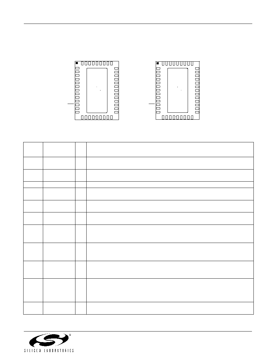
Si2107/08/09/10
Preliminary Rev. 0.7
75
9. Pin Descriptions
Si2108/10
Si2107/09
Pin
Number
Name
I/O
Description
1
VDD_LNA
I
Supply Voltage.
LNA power supply. Connect to 3.3 V.
2
REXT
I/O
External Reference Resistor.
Connect 4.53 k
to GND.
3
ADDR
I/O I2C Address Select.
4
VDD_MIX
I
Supply Voltage.
Mixer power supply. Connect to 3.3 V
5
VDD_BB
I
Supply Voltage.
Baseband power supply. Connect to 1.8 V.
6
VDD_ADC
I
Supply Voltage.
ADC power supply. Connect to 3.3 V.
7
VSEN/TDET
I
Voltage Sense/Tone Detect.
VSEN (Si2108/10 only)--Line voltage of LNB supply circuit.
TDET--Detect input of external tone or tone envelope.
8
LNB1/TGEN
O
LNB Control 1/Tone Generation.
LNB1 (Si2108/10 only)--Required connection to LNB supply circuit.
TGEN--Outputs tone or tone envelope.
9
ISEN
I
Current Sense (Si2108/10 only).
Monitors current of LNB supply circuit. When LNB supply circuit is not populated or
when using Si2107/09, leave pin unconnected.
10
LNB2/DRC
I/O
LNB Control 2/Direction Control.
LNB2 (Si2108/10 only)--required connection to LNB supply circuit.
DRC--Outputs signal to indicate message transmission (HIGH) or reception
(LOW).
11
RESET
I
Device Reset.
Active low.
14 15 16 17 18 19 20 21 22
36
37
38
39
40
41
42
43
44
VD
D_
S
Y
N
T
H
VD
D_
L
O
GN
D
RF
I
P
1
RF
I
N
1
RF
I
N
2
RF
I
P
2
VDD_LNA
REXT
ADDR
VDD_MIX
VDD_BB
VDD_ADC
VSEN/TDET
LNB1/TGEN
ISEN
PWM/DCS
VDD_DIG18
TS_
D
AT
A
[
1]
TS_DATA[7]
TS
_
C
L
K
SCL
SDA
TS_SYNC
TS_VAL
TS_ERR
INT/RLK/GPO
VDD_PLL33
XTOUT
VDD_XTAL
XTAL2
XTAL1
RESET
LNB2/DRC
TS_
D
AT
A
[
0]
TS_
D
AT
A
[
3]
TS_
D
AT
A
[
2]
TS_
D
AT
A
[
4]
TS_
D
AT
A
[
5]
TS_DATA[6]
VD
D_
D
I
G
3
3
VD
D_
D
I
G
3
3
GN
D
GN
D
Top
View
1
2
3
4
5
6
7
8
9
10
11
12
13
23
24
25
26
27
28
29
30
31
32
33
34
35
GND
GND
14 15 16 17 18 19 20 21 22
36
37
38
39
40
41
42
43
44
VD
D_
S
Y
NT
H
VD
D_
L
O
GN
D
RF
IP
1
RF
IN
1
RF
IN
2
RF
IP
2
VDD_LNA
REXT
ADDR
VDD_MIX
VDD_BB
VDD_ADC
TDET
TGEN
NC
DCS
VDD_DIG18
T
S
_
D
ATA[
1
]
TS_DATA[7]
T
S
_CLK
SCL
SDA
TS_SYNC
TS_VAL
TS_ERR
INT/RLK/GPO
VDD_PLL33
XTOUT
VDD_XTAL
XTAL2
XTAL1
RESET
DRC
T
S
_
D
ATA[
0
]
T
S
_
D
ATA[
3
]
T
S
_
D
ATA[
2
]
T
S
_
D
ATA[
4
]
T
S
_
D
ATA[
5
]
TS_DATA[6]
VD
D
_
D
I
G
3
3
VD
D
_
D
I
G
3
3
GN
D
GN
D
Top
View
1
2
3
4
5
6
7
8
9
10
11
12
13
23
24
25
26
27
28
29
30
31
32
33
34
35
GND
GND

Si2107/08/09/10
76
Preliminary Rev. 0.7
12
PWM/DCS
O
PWM/DC Voltage Select.
PWM (Si2108/10 only)--Connected to gate of power MOSFET for LNB supply cir-
cuit.
DCS--Outputs signal to indicate 18 V (HIGH) or 13 V (LOW) LNB supply voltage
selection.
13
VDD_DIG18
I
Supply voltage.
Digital power supply. Connect to 1.8 V.
14≠17,
21≠24
TS_DATA[7:0]
O
Transport Stream Data Bus.
Serial data is output on TS_DATA[0].
18, 20
VDD_DIG33
I
Supply Voltage.
Digital power supply. Connect to 3.3 V.
19
TS_CLK
O Transport Stream Clock.
25
SCL
I
I2C Clock.
26
SDA
I/O I2C Data.
27
TS_SYNC
O Transport Stream Sync.
28
TS_VAL
O Transport Stream Valid.
29
TS_ERR
O Transport Stream Error.
30
INT / RLK /
GPO
O
Multi Purpose Output Pin.
This pin can be configured to one of the following outputs using the Pin Ctrl 2 (05h)
register.
INT = Interrupt
RLK = Receiver lock indicator
GPO = General purpose output
31
VDD_PLL33
I
Supply Voltage.
Analog PLL power supply. Connect to 3.3 V.
32
XTOUT
O
No Connect/Crystal oscillator output.
If this device is to be used as the clock master in a multi-channel design, this pin
should be connect to the XTAL1 pin of a clock slave device. (Otherwise, this pin
should be left unconnected.)
33
VDD_XTAL
I
Supply Voltage.
Crystal Oscillator power supply. Connect to 3.3 V.
34
XTAL2
O
Crystal Oscillator.
Connect to 20 MHz crystal unit.
35
XTAL1
I
Crystal Oscillator.
Connect to 20 MHz crystal unit.
36
VDD_SYNTH
I
Supply Voltage.
Synth power supply. Connect to 3.3 V.
37
VDD_LO
I
Supply Voltage.
Local Oscillator power supply. Connect to 3.3 V.
38,41,44
GND
I
Ground.
Reference ground.
39, 43
RFIP1, RFIP2
I
RF Input.
These pins must be connected together on the board.
40, 42
RFIN1, RFIN2
I
RF Input.
These pins must be connected together on the board.
ePad
GND
I
Ground.
Reference ground.

Si2107/08/09/10
Preliminary Rev. 0.7
77
10. Ordering Guide
1,2
Ordering Part #
Description
Temperature
Si2110-X-FM
Satellite receiver for DVB-S/DSS with LNB step-up dc-dc controller
and on-chip blindscan accelerator, Lead-free and RoHS Compliant
0 to 70
∞C
Si2109-X-FM
Satellite receiver for DVB-S/DSS with on-chip blindscan accelerator,
Lead-free and RoHS Compliant
0 to 70
∞C
Si2108-X-FM
Satellite receiver for DVB-S/DSS with step-up dc-dc controller, Lead-
free and RoHS Compliant
0 to 70
∞C
Si2107-X-FM
Satellite receiver for DVB-S/DSS, Lead-free and RoHS Compliant
0 to 70
∞C
Notes:
1. "X" denotes product revision.
2. Add an "R" at the end of the device to denote tape and reel option; 2500 quantity per reel.
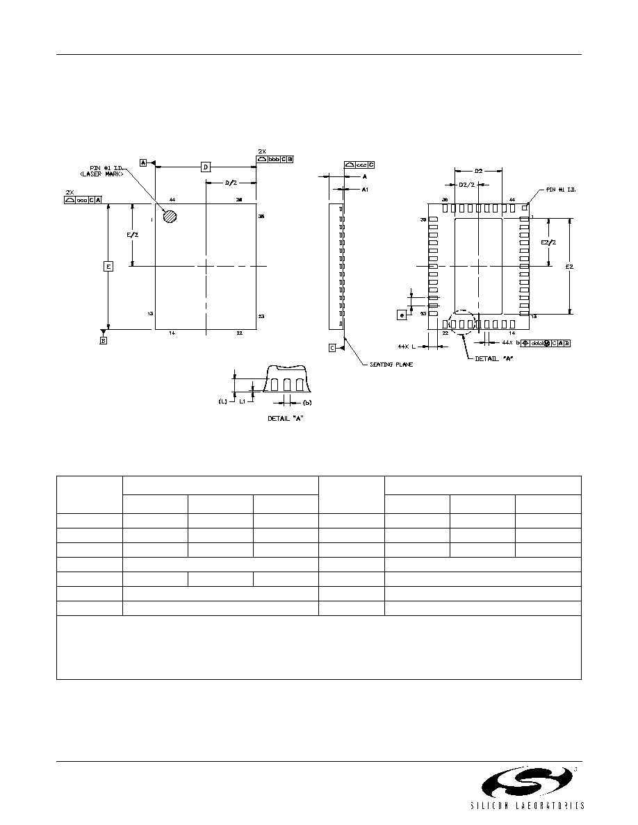
Si2107/08/09/10
78
Preliminary Rev. 0.7
11. Package Outline: 44-pin QFN
Figure 18 illustrates the package details for the Si2110. Table 20 lists the values for the dimensions shown in the
illustration.
Figure 18. 44-Pin QFN
Table 20. Package Diagram Dimensions
Dimension
Millimeters
Dimension
Millimeters
Min
Nom
Max
Min
Nom
Max
A
0.80
0.90
1.00
E2
6.00
6.10
6.20
A1
0.00
0.02
0.05
L
0.45
0.55
0.65
b
0.18
0.25
0.30
L1
0.03
0.05
0.08
D
6.00 BSC.
aaa
0.10
D2
2.70
2.80
2.90
bbb
0.10
e
0.50 BSC.
ccc
0.08
E
8.00 BSC.
ddd
0.10
Notes:
1. Dimensioning and tolerancing per ANSI Y14.5M-1994.
2. This drawing conforms to the JEDEC Solid State Outline MO-220, Variation VJLD.
3. Recommended card reflow profile is per the JEDEC/IPC J-STD-020C specification for small body Components.
4. The pin 1 I.D. pad is for component orientation only and is not to be soldered to the PCB.

Si2107/08/09/10
Preliminary Rev. 0.7
79
D
OCUMENT
C
HANGE
L
IST
Revision 0.4 to Revision 0.5
Package dimensions changed to 6 x 8 mm.
Updated pin numbering and pin descriptions.
Schematics updated.
I2C interface description added.
MPEG-TS timing specifications added.
Revision 0.5 to revision 0.6
Data sheet for Si2107/08/09/10.
Added detailed operational description.
Register map changed for Rev. C silicon.
Various editorial changes and corrections.
Revision 0.6 to revision 0.7
Updated application diagram and BOM.
Added table for multi-device I2C address support.

Si2107/08/09/10
80
Preliminary Rev. 0.7
C
ONTACT
I
NFORMATION
Silicon Laboratories Inc.
4635 Boston Lane
Austin, TX 78735
Tel: 1+(512) 416-8500
Fax: 1+(512) 416-9669
Toll Free: 1+(877) 444-3032
Email: DBSinfo@silabs.com
Internet: www.silabs.com
Silicon Laboratories and Silicon Labs are trademarks of Silicon Laboratories Inc.
Other products or brandnames mentioned herein are trademarks or registered trademarks of their respective holders.
The information in this document is believed to be accurate in all respects at the time of publication but is subject to change without notice.
Silicon Laboratories assumes no responsibility for errors and omissions, and disclaims responsibility for any consequences resulting from
the use of information included herein. Additionally, Silicon Laboratories assumes no responsibility for the functioning of undescribed features
or parameters. Silicon Laboratories reserves the right to make changes without further notice. Silicon Laboratories makes no warranty, rep-
resentation or guarantee regarding the suitability of its products for any particular purpose, nor does Silicon Laboratories assume any liability
arising out of the application or use of any product or circuit, and specifically disclaims any and all liability, including without limitation conse-
quential or incidental damages. Silicon Laboratories products are not designed, intended, or authorized for use in applications intended to
support or sustain life, or for any other application in which the failure of the Silicon Laboratories product could create a situation where per-
sonal injury or death may occur. Should Buyer purchase or use Silicon Laboratories products for any such unintended or unauthorized ap-
plication, Buyer shall indemnify and hold Silicon Laboratories harmless against all claims and damages.