Preliminary Rev. 0.96 2/05
Copyright � 2005 by Silicon Laboratories
Si3232
This information applies to a product under development. Its characteristics and specifications are subject to change without notice.
Si3232
D
U A L
P
R O G R A M M A B L E
CMOS SLIC
W I T H
L
I N E
M
O N I T O R I N G
Features
Applications
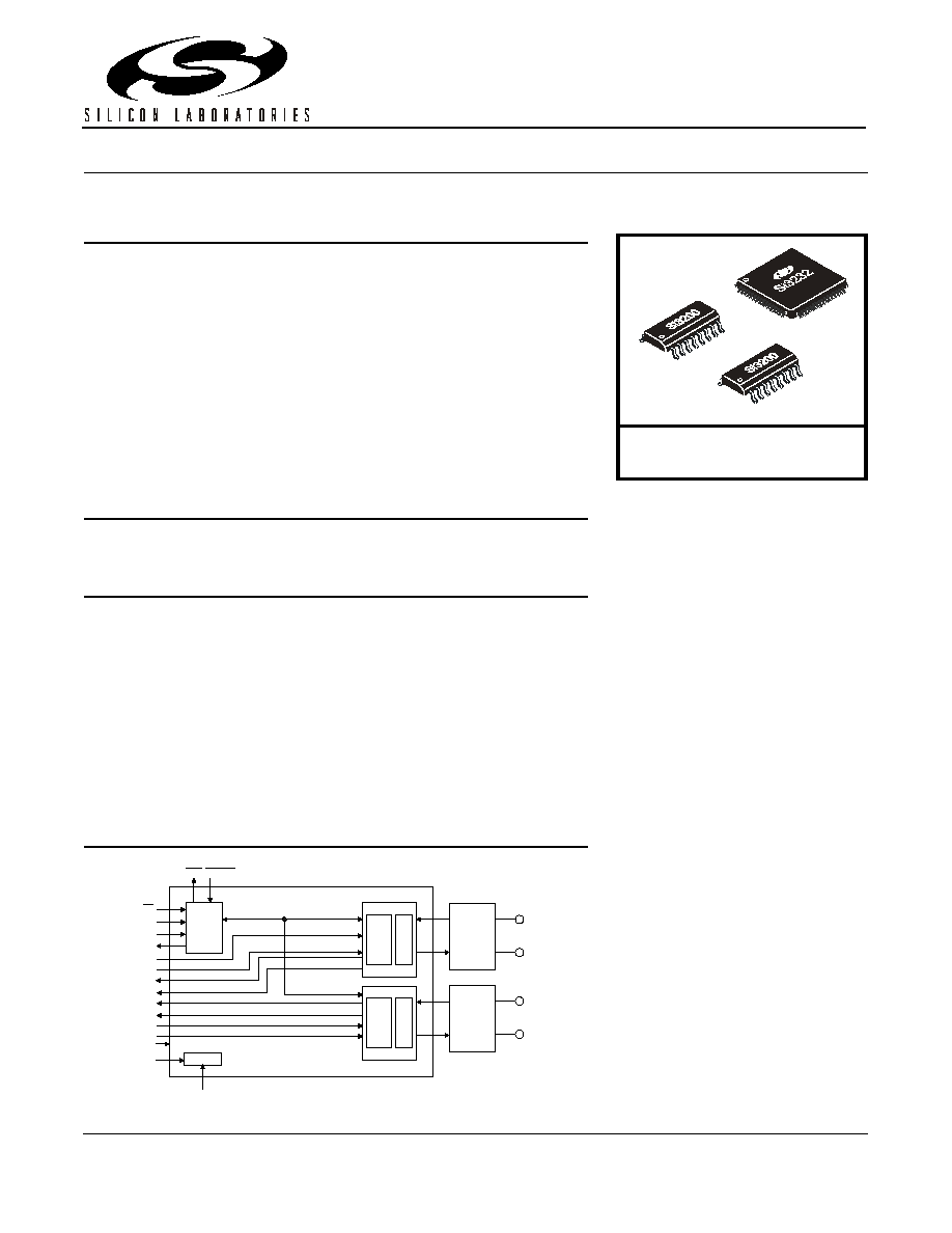
Description
The Si3232 is a low-voltage CMOS SLIC that offers a low-cost, fully software-
programmable, dual-channel, analog telephone interface for customer premise
(CPE) applications. Internal ringing generation eliminates centralized ringers and
ringing relays, and on-chip subscriber loop testing allows remote line card and
loop diagnostics with no external test equipment or relays. The Si3232 performs
all programmable SLIC functions in compliance with all relevant LSSGR, ITU, and
ETSI specifications; all high-voltage functions are performed by the Si3200
linefeed interface IC. The Si3232 operates from a single 3.3 V supply and
interfaces to a standard SPI bus digital interface for control. The Si3200 operates
from a 3.3 V supply as well as high-voltage battery supplies up to 100 V. The
Si3232 is available in a 64-pin thin quad flat package (TQFP), and the Si3200 is
available in a thermally-enhanced 16-pin small-outline (SOIC) package.
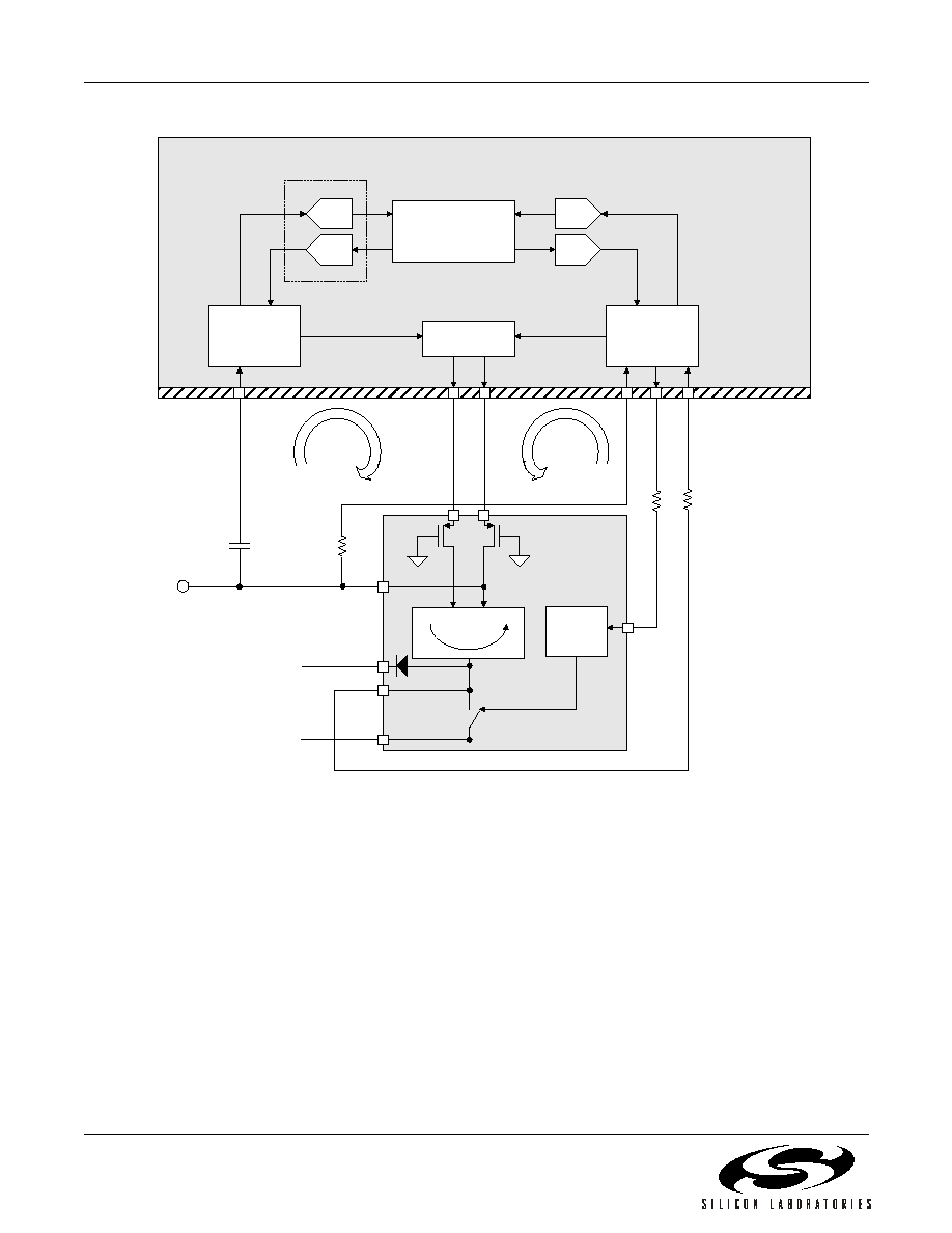
Functional Block Diagram
Ideal for customer premise applications
Low standby power consumption:
<65 mW per channel
Internal balanced ringing to 65 V
rms
Software programmable parameters:
Ringing frequency, amplitude,
cadence, and waveshape
Two-wire ac impedance
DC loop feed (18�45 mA)
Loop closure and ring trip thresholds
Ground key detect threshold
Automatic switching of up to three
battery supplies
On-hook transmission
Loop or ground start operation with
smooth/abrupt polarity reversal
SPI bus digital interface with
programmable interrupts
3.3 V operation
GR-909 loop diagnostics and
loopback testing
12 kHz/16 kHz pulse metering
Lead-free/RoHS compatible
packages available
Cable telephony
Wireless local loop
Voice over IP/voice over DSL
ISDN terminal adapters
L
i
ne
f
e
ed
& M
o
n
i
t
o
r
Ring
Sou
r
c
e
Li
nefe
e
d
& Mo
nitor
Ring
Sou
r
c
e
Si3200
Linefeed
Interface
Si3200
Linefeed
Interface
TIP
RING
TIP
RING
INT RESET
SPI
Control
Interface
SCLK
SDI
CS
VRXPa
VRXNa
VTXPb
VTXNb
VTXPa
VTXNa
VRXPb
VRXNb
PLL
PCLK
Si3232
VCM
SDO
FSYNC
U.S. Patent #6,567,521
U.S. Patent #6,812,744
Other patents pending
Ordering Information
See page 122.

Si3232
2
Preliminary Rev. 0.96

Si3232
Preliminary Rev. 0.96
3
T
A B L E
O F
C
O N T E N TS
Section
Page
1. Electrical Specifications . . . . . . . . . . . . . . . . . . . . . . . . . . . . . . . . . . . . . . . . . . . . . . . . . . .4
2. Typical Application Schematic . . . . . . . . . . . . . . . . . . . . . . . . . . . . . . . . . . . . . . . . . . . . .17
3. Bill of Materials . . . . . . . . . . . . . . . . . . . . . . . . . . . . . . . . . . . . . . . . . . . . . . . . . . . . . . . . . .18
4. Functional Description . . . . . . . . . . . . . . . . . . . . . . . . . . . . . . . . . . . . . . . . . . . . . . . . . . .19
4.1. Linefeed Architecture . . . . . . . . . . . . . . . . . . . . . . . . . . . . . . . . . . . . . . . . . . . . . . . .19
4.2. Power Supply Transients on the Si3200 . . . . . . . . . . . . . . . . . . . . . . . . . . . . . . . . . .19
4.3. DC Feed Characteristics . . . . . . . . . . . . . . . . . . . . . . . . . . . . . . . . . . . . . . . . . . . . . .20
4.4. Linefeed Calibration . . . . . . . . . . . . . . . . . . . . . . . . . . . . . . . . . . . . . . . . . . . . . . . . .25
4.5. Automatic Dual Battery Switching . . . . . . . . . . . . . . . . . . . . . . . . . . . . . . . . . . . . . . .29
4.6. Ringing Generation . . . . . . . . . . . . . . . . . . . . . . . . . . . . . . . . . . . . . . . . . . . . . . . . . .37
4.7. Internal Unbalanced Ringing . . . . . . . . . . . . . . . . . . . . . . . . . . . . . . . . . . . . . . . . . . .39
4.8. Ring Trip Detection . . . . . . . . . . . . . . . . . . . . . . . . . . . . . . . . . . . . . . . . . . . . . . . . . .41
4.9. Ring Trip Timeout Counter . . . . . . . . . . . . . . . . . . . . . . . . . . . . . . . . . . . . . . . . . . . .41
4.10. Ring Trip Debounce Interval . . . . . . . . . . . . . . . . . . . . . . . . . . . . . . . . . . . . . . . . . .41
4.11. Loop Closure Mask . . . . . . . . . . . . . . . . . . . . . . . . . . . . . . . . . . . . . . . . . . . . . . . . .42
4.12. Relay Driver Considerations . . . . . . . . . . . . . . . . . . . . . . . . . . . . . . . . . . . . . . . . . .44
4.13. Two-Wire Impedance Synthesis . . . . . . . . . . . . . . . . . . . . . . . . . . . . . . . . . . . . . . .46
4.14. Audio Path Processing . . . . . . . . . . . . . . . . . . . . . . . . . . . . . . . . . . . . . . . . . . . . . .48
4.15. System Clock Generation . . . . . . . . . . . . . . . . . . . . . . . . . . . . . . . . . . . . . . . . . . . .49
4.16. SPI Control Interface . . . . . . . . . . . . . . . . . . . . . . . . . . . . . . . . . . . . . . . . . . . . . . . .50
4.17. Si3232 RAM and Register Space . . . . . . . . . . . . . . . . . . . . . . . . . . . . . . . . . . . . . .52
4.18. System Testing . . . . . . . . . . . . . . . . . . . . . . . . . . . . . . . . . . . . . . . . . . . . . . . . . . . .57
5. 8-Bit Control Register Summary . . . . . . . . . . . . . . . . . . . . . . . . . . . . . . . . . . . . . . . . . . . .61
6. 8-Bit Control Descriptions . . . . . . . . . . . . . . . . . . . . . . . . . . . . . . . . . . . . . . . . . . . . . . . . .63
7. 16-Bit RAM Address Summary . . . . . . . . . . . . . . . . . . . . . . . . . . . . . . . . . . . . . . . . . . . . .90
8. 16-Bit Control Descriptions . . . . . . . . . . . . . . . . . . . . . . . . . . . . . . . . . . . . . . . . . . . . . . . .93
9. Pin Descriptions: Si3232 . . . . . . . . . . . . . . . . . . . . . . . . . . . . . . . . . . . . . . . . . . . . . . . . .117
10. Pin Descriptions: Si3200 . . . . . . . . . . . . . . . . . . . . . . . . . . . . . . . . . . . . . . . . . . . . . . . .120
11. Ordering Guide . . . . . . . . . . . . . . . . . . . . . . . . . . . . . . . . . . . . . . . . . . . . . . . . . . . . . . . .122
12. Product Identification . . . . . . . . . . . . . . . . . . . . . . . . . . . . . . . . . . . . . . . . . . . . . . . . . .122
12.1. Part Designators (Partial List) . . . . . . . . . . . . . . . . . . . . . . . . . . . . . . . . . . . . . . . .122
13. Package Outline: 64-Pin eTQFP . . . . . . . . . . . . . . . . . . . . . . . . . . . . . . . . . . . . . . . . . .123
14. Package Outline: 16-Pin ESOIC . . . . . . . . . . . . . . . . . . . . . . . . . . . . . . . . . . . . . . . . . .124
Support Documentation . . . . . . . . . . . . . . . . . . . . . . . . . . . . . . . . . . . . . . . . . . . . . . . . . . .125
Document Change List . . . . . . . . . . . . . . . . . . . . . . . . . . . . . . . . . . . . . . . . . . . . . . . . . . . .126
Contact Information . . . . . . . . . . . . . . . . . . . . . . . . . . . . . . . . . . . . . . . . . . . . . . . . . . . . . . .128

Si3232
4
Preliminary Rev. 0.96
1. Electrical Specifications
Table 1. Absolute Maximum Ratings and Thermal Information
1
Parameter
Symbol
Test Condition
Value
Unit
Supply Voltage, Si3200 and Si3232
V
DD
, V
DD1
�V
DD4
�0.5 to 6.0
V
High Battery Supply Voltage
2
V
BATH
Continuous
0.4 to �104
V
10 ms
0.4 to �109
Low Battery Supply Voltage, Si3200
2
V
BAT
,
V
BATL
Continuous
V
BATH
V
TIP or RING Voltage, Si3200
V
TIP
, V
RING
Continuous
Pulse < 10
�s
Pulse < 4
�s
�104
V
BATH
�15
V
BATH
�35
V
V
V
TIP, RING Current, Si3200
I
TIP
, I
RING
�100
mA
STIPAC, STIPDC, SRINGAC,
SRINGDC Current, Si3232
�20
mA
Input Current, Digital Input Pins
I
IN
Continuous
�10
mA
Digital Input Voltage
V
IND
�0.3 to (
V
DD
+ 0.3)
V
Operating Temperature Range
T
A
�40 to 100
�C
Storage Temperature Range
T
STG
�40 to 150
�C
Si3232 Thermal Resistance, Typical
3
(TQFP-64 ePad)
JA
25
�C/W
Si3200 Thermal Resistance, Typical
3
(SOIC-16 ePad)
JA
55
�C/W
Continuous Power Dissipation,
Si3200
4
P
D
T
A
= 85 �C, SOIC-16
1
W
Continuous Power Dissipation,
Si3232
P
D
T
A
= 85 �C, TQFP-64
1.6
W
Notes:
1. Permanent device damage may occur if the above Absolute Maximum Ratings are exceeded. Functional operation
should be restricted to the conditions as specified in the operational sections of this data sheet. Exposure to absolute
maximum rating conditions for extended periods may affect device reliability.
2. The dv/dt of the voltage applied to the V
BAT
, V
BATH
, and V
BATL
pins must be limited to 10 V/
�s.
3. The thermal resistance of an exposed pad package is assured when the recommended PCB layout guidelines are
followed correctly. The specified performance requires that the exposed pad be soldered to an exposed copper surface
of equal size and that multiple vias are added to enable heat transfer between the top-side copper surface and a large
internal copper ground plane. Refer to "AN55: Dual ProSLICTM User Guide" or to the Si3232 evaluation board data
sheet for specific layout examples.
4. On-chip thermal limiting circuitry will shut down the circuit at a junction temperature of approximately 150 �C. For
optimal reliability, operation above 140 �C junction temperature should be avoided.

Si3232
Preliminary Rev. 0.96
5
Table 2. Recommended Operating Conditions
Parameter
Symbol
Test
Condition
Min*
Typ
Max*
Unit
Ambient Temperature
T
A
K-grade
0
25
70
o
C
Ambient Temperature
T
A
B-grade
�40
25
85
o
C
Si3232 Supply Voltage
V
DD1
�V
DD4
3.13
3.3
3.47
V
Si3200 Supply Voltage
V
DD
3.13 3.3
3.47
V
High Battery Supply Voltage, Si3200
V
BATH
�15
--
�99
V
Low Battery Supply Voltage, Si3200
V
BATL
�15
--
V
BATH
V
*Note: All minimum and maximum specifications are guaranteed and apply across the recommended operating conditions.
Typical values apply at nominal supply voltages and an operating temperature of 25
o
C unless otherwise stated.

Si3232
6
Preliminary Rev. 0.96
Table 3. Power Supply Characteristics
1
(V
DD
, V
DD1
�V
DD4
=
3.3 V, T
A
=
0 to 70 �C for K-Grade, �40 to 85 �C for B-Grade)
Parameter
Symbol
Test Condition
Min
Typ
Max
Unit
V
DD1
�V
DD4
Supply Current
(Si3232)
I
VDD1
�I
VDD4
Sleep mode, RESET = 0
--
1
--
mA
Open (high impedance)
--
15
--
mA
Active on-hook standby
--
15
--
mA
Forward/reverse active off-hook
ABIAS = 4 mA
--
20
--
mA
Forward/reverse active OHT
OBIAS = 4 mA
--
12 +
I
LIM
--
mA
Ringing, V
RING
= 45 V
rms
,
V
BAT
= �70 V, Sine Wave, 1 REN load
2
--
28
--
mA
V
DD
Supply
Current (Si3200)
I
VDD
Sleep mode, RESET = 0
--
100
--
�A
Open (high impedance)
--
100
--
�A
Active on-hook standby
--
110
--
�A
Forward/reverse active off-hook,
ABIAS = 4 mA, V
BAT
= �24 V
--
110
--
�A
Forward/reverse OHT, OBIAS = 4 mA,
V
BAT
= �70 V
--
110
--
�A
Ringing, V
RING
= 45 V
rms
,
VBAT = �70 V, Sine Wave, 7 REN load
--
110
--
�A
V
BAT
Supply
Current (Si3200)
I
VBAT
Sleep mode, RESET = 0, V
BAT
= �70 V
--
100
--
�A
Open (high impedance), V
BAT
= �70 V
--
225
--
�A
Active on-hook standby, V
BAT
= �70 V
--
400
--
�A
Forward/reverse active off-hook,
ABIAS = 4 mA, V
BAT
= �24 V
--
4.4 +
I
LIM
--
mA
Forward/reverse OHT, OBIAS = 4 mA,
V
BAT
= �70 V
--
8.4
--
mA
Ringing, V
RING
= 45 V
rms
,
V
BAT
= �70 V, Sine wave, 1 REN load
2
--
6
--
mA
Notes:
1. All specifications are for a single channel based on measurements with both channels in the same operating state.
2. See "4.7.4. Ringing Power Considerations" for current and power consumption under other operating conditions.
3. Power consumption does not include additional power required for dc loop feed. Total system power consumption must
include an additional V
BAT
x I
LIM
term.

Si3232
Preliminary Rev. 0.96
7
Power Consumption
P
SLEEP
Sleep mode, RESET = 0, V
BAT
= �70 V
--
8
--
mW
P
OPEN
Open (high impedance), V
BAT
= �70 V
--
65
--
mW
P
STBY
Active on-hook standby, V
BAT
= �48 V
--
70
--
mW
P
STBY
Active on-hook standby, V
BAT
= �70 V
--
80
--
mW
P
ACTIVE
3
Forward/reverse active off-hook,
ABIAS = 4 mA, V
BAT
= �24 V
--
175
--
mW
P
ACTIVE
3
Forward/reverse active off-hook,
ABIAS = 4 mA, V
BAT
= �48 V
--
280
--
mW
P
OHT
Forward/reverse OHT, OBIAS = 4 mA,
V
BAT
= �48 V
--
500
--
mW
P
OHT
Forward/reverse OHT, OBIAS = 4 mA,
V
BAT
= �70 V
--
685
--
mW
P
RING
Ringing, V
RING
= 45 V
rms
,
V
BAT
= �70 V, Sine Wave, 1 REN load
2
--
516
--
mW
Table 3. Power Supply Characteristics
1
(Continued)
(V
DD
, V
DD1
�V
DD4
=
3.3 V, T
A
=
0 to 70 �C for K-Grade, �40 to 85 �C for B-Grade)
Parameter
Symbol
Test Condition
Min
Typ
Max
Unit
Notes:
1. All specifications are for a single channel based on measurements with both channels in the same operating state.
2. See "4.7.4. Ringing Power Considerations" for current and power consumption under other operating conditions.
3. Power consumption does not include additional power required for dc loop feed. Total system power consumption must
include an additional V
BAT
x I
LIM
term.

Si3232
8
Preliminary Rev. 0.96
Table 4. AC Characteristics
(V
DD
, V
DD1
�V
DD4
=
3.13 to 3.47 V, T
A
=
0 to 70 �C for K-Grade, �40 to 85 �C for B-Grade)
Parameter
Test Condition
Min
Typ
Max
Unit
TX/RX Performance
TX Full Scale Output
VTXP�XTXN
0.1
--
V
DD
�0.1
V
RX Full Scale Input
VRXP�VRXN, ARX = 0 dB
ARX = �3.52 dB
ARX = �6.02 dB
0.25
0
0
--
--
--
V
DD
�0.25
V
DD
V
DD
V
V
V
Analog Input/Output Common
Mode Voltage
CMTXSEL = 1
CMTXSEL = 0
0.6
--
--
1.5
1.5
--
V
V
Overload Level
ATX stage = 0 dB, THD = 1.5%
2.5
--
--
V
PK
Overload Compression
Figure 4
--
--
Single Frequency Distortion
1
2-wire to 4-wire or 4-wire to 2-wire:
200 Hz�3.4 kHz
--
�74
�68
dB
2-wire to 4-wire to 2-wire:
200 Hz�3.4 kHz
--
�74
�65
dB
Signal-to-(Noise + Distortion)
Ratio
2
200 Hz�3.4 kHz
Active off-hook, and OHT, any Z
T
--
�74
�68
Intermodulation Distortion
--
--
�41
dB
Gain Accuracy
2
2-Wire to 4-Wire or 4-Wire to 2-Wire,
1014 Hz, Any gain setting
�0.25
--
+0.25
dB
Gain Distortion vs. Frequency
�3 dB corners
0.01
--
10
kHz
Gain Tracking
1014 Hz sine wave,
reference level �10 dBm
signal level:
3 dB to �37 dB
�37 dB to �50 dB
�50 dB to �60 dB
--
--
--
--
--
--
�0.25
�0.5
�1.0
dB
dB
dB
Crosstalk between channels
TX or RX to TX
TX to RX to RX
0 dBm0,
300 Hz to 3.4 kHz
300 Hz to 3.4 kHz
--
--
--
--
�75
�75
dB
dB
2-Wire Return Loss
3
200 Hz to 3.4 kHz
26
30
--
dB
Notes:
1. The input signal level should be 0 dBm0 for frequencies greater than 100 Hz. For 100 Hz and below, the level should
be �10 dBm0. The output signal magnitude at any other frequency will be smaller than the maximum value
specified.
2. Analog signal measured as V
TIP
� V
RING
. Assumes ideal line impedance matching.
3. V
DD
=
3.3 V, V
BAT
=
�52 V, no fuse resistors, R
L
=
600
, Z
S
=
600
synthesized using RS register coefficients.
4. The level of any unwanted tones within the bandwidth of 0 to 4 kHz will not exceed �55 dBm.
5. The OBIAS and ABIAS registers program the dc bias current through the SLIC in the on-hook transmission and off-
hook active conditions, respectively. This per-pin total current setting should be selected such that it can
accommodate the sum of the metallic and longitudinal currents through each of the TIP and RING leads for a given
application.

Si3232
Preliminary Rev. 0.96
9
Noise Performance
Idle Channel Noise
4
C-Message weighted
--
12
15
dBrnC
Psophometric weighted
--
�78
�75
dBmP
3 kHz flat
--
--
18
dBrn
PSRR from V
DD1
� V
DD4
RX and TX, dc to 3.4 kHz
40
--
--
dB
PSRR from V
BAT
RX and TX, dc to 3.4 kHz
60
--
--
dB
Longitudinal Performance
Longitudinal to Metallic Bal-
ance (forward or reverse)
200 Hz to 1 kHz
58
63
--
dB
1 kHz to 3.4 kHz
53
58
--
dB
Metallic to Longitudinal Bal-
ance
200 Hz to 3.4 kHz
40
--
--
dB
Longitudinal Impedance
5
200 Hz to 3.4 kHz at TIP or RING
Register-dependent
OBIAS/ABIAS
00 = 4 mA
01 = 8 mA
10 = 12 mA
11 = 16 mA
--
--
--
--
50
25
25
20
--
--
--
--
Longitudinal Current per Pin
5
Active off-hook
200 Hz to 3.4 kHz
Register-dependent
OBIAS/ABIAS
00 = 4 mA
01 = 8 mA
10 = 12 mA
11 = 16 mA
--
--
--
--
4
8
8
10
--
--
--
--
mA
mA
mA
mA
Table 4. AC Characteristics (Continued)
(V
DD
, V
DD1
�V
DD4
=
3.13 to 3.47 V, T
A
=
0 to 70 �C for K-Grade, �40 to 85 �C for B-Grade)
Parameter
Test Condition
Min
Typ
Max
Unit
Notes:
1. The input signal level should be 0 dBm0 for frequencies greater than 100 Hz. For 100 Hz and below, the level should
be �10 dBm0. The output signal magnitude at any other frequency will be smaller than the maximum value
specified.
2. Analog signal measured as V
TIP
� V
RING
. Assumes ideal line impedance matching.
3. V
DD
=
3.3 V, V
BAT
=
�52 V, no fuse resistors, R
L
=
600
, Z
S
=
600
synthesized using RS register coefficients.
4. The level of any unwanted tones within the bandwidth of 0 to 4 kHz will not exceed �55 dBm.
5. The OBIAS and ABIAS registers program the dc bias current through the SLIC in the on-hook transmission and off-
hook active conditions, respectively. This per-pin total current setting should be selected such that it can
accommodate the sum of the metallic and longitudinal currents through each of the TIP and RING leads for a given
application.

Si3232
10
Preliminary Rev. 0.96
Table 5. Linefeed Characteristics
(V
DD
, V
DD1
�V
DD4
=
3.13 to 3.47 V, T
A
=
0 to 70 �C for K-Grade, �40 to 85 �C for B-Grade)
Parameter
Symbol
Test Condition
Min
Typ
Max
Unit
DC Loop Current Accuracy
I
LIM
= 18 mA
--
--
�10
%
DC Open Circuit Voltage
Accuracy
Active Mode; V
OC
= 48 V,
V
TIP
� V
RING
--
--
�4
V
DC Differential Output
Resistance
R
DO
I
LOOP
< I
LIM
--
320
--
DC On-Hook Voltage
Accuracy--Ground Start
V
OHTO
I
RING
<I
LIM
; V
RING
wrt ground
V
RING
= �51 V
--
--
�4
V
DC Output Resistance--
Ground Start
R
ROTO
I
RING
<I
LIM
; RING to ground
--
320
--
DC Output Resistance--
Ground Start
R
TOTO
TIP to ground
300
--
--
k
Loop Closure Detect
Threshold Accuracy
I
THR
= 13 mA
--
�10
�15
%
Ground Key Detect
Threshold Accuracy
I
THR
= 13 mA
--
�10
�15
%
Ring Trip Threshold
Accuracy
ac Detection, V
RING
= 70 V
PK
,
I
TH
= 80 mA
--
�4
�5
mA
dc detection,
20 V dc offset, I
TH
= 13 mA
--
�1.5
�2
mA
Ringing Amplitude*
V
RING
Open circuit, V
BATH
= 100 V
93
--
--
V
PK
5 REN load, R
LOOP
= 0
,
V
BATH
= 100 V
82
--
--
V
PK
Sinusoidal Ringing Total
Harmonic Distortion
R
THD
--
2
--
%
Ringing Frequency Accuracy
f = 16 Hz to 100 Hz
--
--
�1
%
Ringing Cadence Accuracy
Accuracy of ON/OFF times
--
--
�50
ms
Calibration Time
CAL to CAL bit
--
--
600
ms
Loop Voltage Sense
Accuracy
Accuracy of boundaries for each
output Code;
V
TIP
� V
RING
= 48 V
--
�2
�4
%
Loop Current Sense
Accuracy
Accuracy of boundaries for each
output code;
I
LOOP
= 18 mA
--
�7
�10
%
Power Alarm Threshold
Accuracy
Power Threshold = 300 mW
--
--
�25
%
*Note: Ringing amplitude is set for 93 V peak using the RINGAMP RAM address and measured at TIP-RING using no series
protection resistance.

Si3232
Preliminary Rev. 0.96
11
Table 6. Monitor ADC Characteristics
(V
DD
, V
DD1
�V
DD4
=
3.13 to 3.47 V, T
A
=
0 to 70 �C for K-Grade, �40 to 85 �C for B-Grade)
Parameter
Symbol
Test Condition
Min
Typ
Max
Unit
Resolution
--
8
--
Bits
Differential Nonlinearity
DNL
--
�1.0
�0.75
--
--
+1.5
LSB
LSB
Integral Nonlinearity
INL
--
�0.6
�1.5
LSB
Gain Error
--
�0.1
�0.25
LSB
Table 7. Si3200 Characteristics
(V
DD
=
3.13 to 3.47 V, T
A
=
0 to 70 �C for K-Grade, �40 to 85 �C for B-Grade)
Parameter
Symbol
Test Condition
Min
Typ
Max
Unit
TIP/RING Pulldown Transistor
Saturation Voltage
V
CM
V
RING
� V
BAT
(Forward),
V
TIP
� V
BAT
(Reverse)
I
LIM
= 22 mA, I
ABIAS
= 4 mA
1
I
LIM
= 45 mA, I
ABIAS
= 16 mA
1
3
4
--
V
V
TIP/RING Pullup Transistor
Saturation Voltage
V
OV
GND � V
TIP
(Forward)
GND � V
RING
(Reverse)
I
LIM
= 22 mA
1
I
LIM
= 45 mA
1
3
4
--
V
V
Battery Switch Saturation
Impedance
R
SAT
(V
BAT
� V
BATH
)/I
OUT
(Note 2)
15
W
OPEN State TIP/RING Leakage
Current
I
LKG
R
L
= 0
100
�A
Internal Blocking Diode Forward
Voltage
V
F
V
BAT
� V
BATL
(Note 2)
0.8
V
Notes:
1. V
AC
=
2.5 V
PK
, R
LOAD
=
600
.
2. I
OUT
= 60 mA

Si3232
12
Preliminary Rev. 0.96
Table 8. DC Characteristics, V
DDA
= V
DDD
= V
CC
= 3.3 V
(V
DD
, V
DD1
�V
DD4
= 3.13 V to 3.47 V, T
A
= 0 to 70 �C for K-Grade, �40 to 85 �C for B-Grade)
Parameter
Symbol
Test Condition
Min
Typ
Max
Unit
High Level Input
Voltage
V
IH
0.7 x
V
DD
--
3.47
V
Low Level Input Voltage
V
IL
--
--
0.3 x
V
DD
V
High Level Output
Voltage
V
OH
I
O
= 4 mA
V
DD
� 0.6
--
--
V
Low Level Output
Voltage
V
OL
SDO, INT, SDITHRU
I
O
= �4 mA
--
--
0.4
V
BATSELa/b, GPOa/b:
I
O
= �40 mA
--
--
0.72
V
SDITHRU Internal
Pullup Resistance
35
50
--
k
GPO Relay Driver
Source Impedance
R
OUT
V
DD1
�V
DD4
= 3.13 V,
I
O
< 28 mA
--
63
--
GPO Relay Driver Sink
Impedance
R
IN
V
DD1
�V
DD4
= 3.13 V,
I
O
< 85 mA
--
11
--
Input Leakage Current
I
L
--
--
�10
�A
Note: All timing (except Rise and Fall time) is referenced to the 50% level of the waveform. Input test levels are V
IH
=
V
DD
�
0.4 V, V
IL
=
0.4 V. Rise and Fall times are referenced to the 20% and 80% levels of the waveform.
Table 9. Switching Characteristics--General Inputs
(V
DD
, V
DD1
�V
DD4
=
3.13 to 3.47 V, T
A
=
0 to 70 �C for K-Grade, �40 to 85 �C for B-Grade, C
L
=
20 pF)
Parameter
Symbol
Min
Typ
Max
Unit
Rise Time, RESET
t
r
--
--
5
ns
RESET Pulse Width
*
t
rl
500
--
--
ns
RESET Pulse Width*, SDI Daisy Chain Mode
t
rl
6
--
--
�s
*Note: The minimum RESET pulse width assumes the SDITHRU pin is tied to ground via a pulldown resistor no greater than
10 k
per device.

Si3232
Preliminary Rev. 0.96
13
Figure 1. SPI Timing Diagram
Table 10. Switching Characteristics--SPI
(V
DD
, V
DD1
�V
DD4
=
3.13 to 3.47 V, T
A
=
0 to 70 �C for K-Grade, �40 to 85 �C for B-Grade, C
L
=
20 pF)
Parameter
Symbol
Test
Conditions
Min
Typ
Max
Unit
Cycle Time SCLK
t
c
0.062
--
--
�s
Rise Time, SCLK
t
r
--
--
25
ns
Fall Time, SCLK
t
f
--
--
25
ns
Delay Time, SCLK Fall to SDO
Transition
t
d2
--
--
20
ns
Delay Time, CS Rise to SDO Tristate
t
d3
--
--
20
ns
Setup Time, CS to SCLK Rise
t
su1
15
--
--
ns
Hold Time, SCLK Rise to CS Rise
t
h1
20
--
--
ns
Setup Time, SDI to SCLK Rise
t
su2
25
--
--
ns
Hold Time, SCLK Rise to SDI Rise
t
h2
20
--
--
ns
SDI to SDITHRU Propagation Delay
--
6
--
ns
Note: All timing is referenced to the 50% level of the waveform. Input test levels are V
IH
� V
DD
�0.4 V, V
IL
=
0.4 V
SCLK
CS
SDI
t
h1
t
d3
SDO
t
d2
t
su1
t
r
t
r
t
c
t
su2
t
h2

Si3232
14
Preliminary Rev. 0.96
Figure 2. PCLK, FSYNC Timing Diagram
Table 11. Switching Characteristics--PCLK and FSYNC Timing
(V
DD
, V
DD1
�V
DD4
=
3.13 to 3.47 V, T
A
=
0 to 70 �C for K-Grade, �40 to 85 �C for B-Grade, C
L
=
20 pF)
Parameter
Symbol
Test
Conditions
Min
1
Typ
1
Max
1
Units
PCLK Period
t
p
122
--
3706
ns
Valid PCLK Inputs
--
--
--
--
--
--
--
--
--
256
512
768
1.024
1.536
1.544
2.048
4.096
8.192
--
--
--
--
--
--
--
--
--
kHz
kHz
kHz
MHz
MHz
MHz
MHz
MHz
MHz
FSYNC Period
2
t
fs
--
125
--
�s
PCLK Duty Cycle Tolerance
t
dty
40
50
60
%
PCLK Period Jitter Tolerance
t
jitter
--
--
�120
ns
Rise Time, PCLK
t
r
--
--
25
ns
Fall Time, PCLK
t
f
--
--
25
ns
Setup Time, FSYNC to PCLK Fall
t
su1
25
--
--
ns
Hold Time, FSYNC to PCLK Fall
t
h1
20
--
--
ns
FSYNC Pulse Width
t
wfs
t
p
/2
--
125
�s�t
p
ns
Notes:
1. All timing is referenced to the 50% level of the waveform. Input test levels are V
IH �
V
I/O �
0.4 V, V
IL
=
0.4 V.
2. FSYNC source is assumed to be 8 kHz under all operating conditions.
PCLK
FSYNC
t
r
t
p
t
s u 1
t
f
t
f s
t
h 1

Si3232
Preliminary Rev. 0.96
15
Figure 3. Si3232 Simplified Audio Path Block Diagram
Figure 4. Overload Compression Performance
+
+
Pulse
Metering DAC
I
buf
G
m
Z
A
ATX
TIP/
RING
Pulse Metering
Generation
Mute
Mute
ARX
To off-chip
A/D
Pulse Metering
Detection
D/A
To DSP
Codec
Loopback
From
off-chip
D/A
1
2
3
4
5
6
7
8
9
1
2
3
4
5
6
7
8
9
0
2.6
Acceptable
Region
Fundamental Input Power (dBm0)
Fundamental
Output Power
(dBm0)

Si3232
16
Preliminary Rev. 0.96
Figure 5. Typical Connection Diagram between Si3232 and Broadcom� BCM3341
(One SLIC channel shown: Channel "a")
VRXP
VRXN
VTXP
VTXN
CMlevel
BCM3341
INT
SCLK
CS
SDI
C41 3.3 nF
C42 3.3 nF
C43 3.3 nF
C45 150 pF
C46 150 pF
C47 150 pF
R40
20 k
R41
20 k
SRINGDCa
SRINGACa
STIPDCa
SRINGDACa
ITIPPa
IRINGNa
IRINGPa
ITIPNa
Si
32
00
SPI
Port
Si3232
V
BAT
TIP
RING
VCM
VTXNa
VTXPa
VRXNa
VRXPa
SDO

Si3232
Preliminary Rev. 0.96
17
2. Typical Application Schematic
VRXPa
V
T
XPa
VT
X
N
a
VT
X
P
VRXP
CM
Le
v
e
l
VBLO
DETn
/
R
E
SET
T
IPa
_
EXT
+5V
VRXPb
V
T
XPb
VT
X
N
b
VRXNb
CM
Le
v
e
l
VB
HI
VT
X
N
a
VTXN
VT
X
N
b
VRXNb
V
T
XPa
VT
X
P
V
T
XPb
VRXPa
VRXP
VRXPb
VRXN
VRXNa
VRXNa
DETn
TI
P
b
TI
P
a
RINGa
RINGb
VRXN
VTXN
RI
NGa
_
E
X
T
VDD
VDD
VBL
O
VDD
VDD
VB
HI
VBL
O
VB
HI
SD
I
T
HRU
/R
ES
E
T
/I
NT
TIPa
TIPb
RIN
G
b
/CS
SC
L
K
SD
O
SDI
FSYNC
PC
L
K
RIN
G
a
R
I
NGb_ex
t
R
I
NGa_ex
t
TI
P
b_ex
t
TI
P
a_ex
t
P
r
ot
ect
i
o
n
P
r
ot
ect
i
o
n
VRX
P
VRX
N
C
h
annel
a
b
a
b
VTX
P
VTX
N
GP
O
a
GP
O
b
R10
4
0
.
2
k
TP
1
Tip A
1
TP
2
R
i
ng A
1
TP
3
Tip B
1
TP
4
R
i
ng B
1
C
1
0.
1u
100V
X7
R
TP
5
GND
1
C3
10n
100V
C1
1
0
.
1
u
100V
X7
R
C5
1u
6V
TP
6
GND
1
R2
2
3
9
0
J2
1
2
J1
R
J
-11 S
M
D
1
2
3
4
5
6
C1
2
0
.
1
u
100V
X7
R
R2
4
39
k
C3
2
0.
1u
100V
C3
3
0.
1
u
100V
JC
P
4
con50_c
h
a
m
p
_
m
5-175473-6
AMP
21
22
23
24
25
19
20
5
4
3
2
1
12
11
10
9
8
7
6
18
17
16
15
14
13
26
27
28
29
30
31
32
33
34
35
36
37
38
39
40
41
42
43
44
45
46
47
48
49
50
J11
R
J
-11 S
M
D
1
2
3
4
5
6
TP
8
GND
1
C2
3
0.
1u
C4
10n
100V
C6
1u
6V
C30
0.
1u
100V
C2
4
0.
1u
R2
0
390
C1
6
1u
6V
C31
0.
1u
100V
R
1
1
4
02k
R
1
2
4
02k
C1
3
10n
100V
U1
Si3232
QGND
8
CAPPb
11
STIPDCb
17
VCM
28
VTXNb
32
VTXNa
50
VTXPa
51
VTXPb
31
VRXPa
53
RPOa
2
ITIPNb
21
ITIPPb
23
GND2
25
VDD2
24
STIPACa
63
THERMa
54
SRINGACa
62
IRINGNa
59
IRINGPa
55
ITIPPa
58
CAPPa
6
SRINGDCa
61
VDD1
57
ITIPNa
60
RPIa
3
RNIa
4
STIPACb
18
SRINGACb
19
VRXNa
52
IRINGPb
26
RPOb
15
RNOa
5
CAPMa
7
IRINGNb
22
RPIb
14
STIPDCa
64
GND1
56
SRINGDCb
20
CAPMb
10
IREF
9
RNOb
12
RNIb
13
FSYNC
34
VRXPb
29
VRXNb
30
SVBATa
1
BATSELB
35
SVBATb
16
/CS
47
PCLK
39
SDO
44
GPOb
36
VDD3
37
SDITHRU
46
THERMb
27
SDI
45
GND3
38
/RST
33
SCLK
43
BATSELa
49
VDD4
42
/INT
40
GPOa
48
GND4
41
C1
5
1u
6V
R2
3
15
R
1
3
4.
7k
R7
182
R
1
4
4.
7k
C
2
0.
1u
100V
X7
R
R
1
5
806
k
R18
1
8
2
TP7
GND
1
U2
Si3200
TIP
1
NC
2
RING
3
VBAT
4
VBATH
5
VBATL
6
GND
7
VDD
8
NC
11
NC
10
BATSEL
9
IRINGP
13
IRINGN
12
THERM
14
ITIPP
16
ITIPN
15
GND
epad
R17
1
8
2
U3
Si3200
TIP
1
NC
2
RING
3
VBAT
4
VBATH
5
VBATL
6
GND
7
VDD
8
NC
11
NC
10
BATSEL
9
IRINGP
13
IRINGN
12
THERM
14
ITIPP
16
ITIPN
15
GND
epad
R
1
402
k
R
2
402
k
JP
3
1
1
2
2
3
3
4
4
5
5
6
6
R4
4
.
7
k
JP
4
1
1
2
2
3
3
4
4
5
5
6
6
R2
1
15
R3
4
.
7
k
R8
182
R6
4
0
.
2
k
R
5
806
k
J3
1
2
R16
4
0
.
2
k
C1
4
10n
100V

Si3232
18
Preliminary Rev. 0.96
3. Bill of Materials
Component
Value
Function
C1, C2, C11, C12
100 nF, 100 V, X7R, �20%
Filter capacitors for TIP, RING ac-sensing inputs.
C3, C4, C13, C14
10 nF, 100 V, X7R, �20%
TIP/RING compensation capacitors.
C5, C6, C15, C16
1 �F, 10 V, X7R, �20%
Low-pass filter capacitor to stabilize differential and
common mode SLIC feedback loops.
C20�C25
0.1 �F, 10 V, Y5V
Decoupling for analog and digital chip supply pins.
C30�C33
0.1 �F, 100 V, Y5V
Decoupling for battery voltage supply pins.
C41�43*
3.3 nF, 10 V, X7R, �20%
Reconstruction filter for DAC of BCM3341.
C45�47*
150 nF, 10 V, X7R, �20%
Anti-aliasing filter for ADC of BCM3341.
R1, R2, R11, R12
402 k
, 1/10 W, �1%
Sense resistors for TIP, RING dc sensing nodes.
R3, R4, R13, R14
4.7 k
, 1/10 W, �5%
Current limiting resistors for TIP, RING ac-sensing
inputs.
R5, R15
806 k
, 1/10 W, �1%
Sense resistor for battery voltage sensing node.
R6, R16
40.2 k
, 1/10 W, �5%
Sets bias current for battery switching logic circuit.
R7, R8, R17, R18
182
, 1/10 W, �1%
Reference resistors for internal transconductance
amplifier.
R10
40.2 k
, 1/10 W, �1%
Generates a high accuracy reference current.
R40, R41*
20 k
, 1/10 W, �1%
Anti-aliasing filter for ADC of BCM3341.
*Note: These components are only required when used with BCM3341 and other interface-compatible Broadcom products.

Si3232
Preliminary Rev. 0.96
19
4. Functional Description
The Si3232 dual SLIC is a low-voltage CMOS device
that provides a fully-programmable SLIC with line
monitoring and test functions to create a dual-channel
analog telephone interface. Intended for multiple
channel applications, the Si3232 provides high
integration and low-power operation for applications,
such as integrated access devices (IADs), voice-over
DSL systems, cable telephony systems, and voice-over
IP systems. These devices meet all relevant Bellcore
LSSGR, ITU, and ETSI standards.
The Si3232 performs the battery, overvoltage, ringing,
supervision, hybrid, and test functions on-chip in a low-
power, small-footprint solution. All high-voltage
functions are implemented using the Si3200 linefeed
interface IC allowing a highly-integrated solution that
offers the lowest total system cost.
The internal linefeed circuitry provides programmable
on-hook voltage and off-hook loop current, reverse
battery operation, loop or ground start operation, and
on-hook transmission. Loop current and voltage are
continuously monitored using an integrated 8-bit
monitor A/D converter. The Si3232 provides on-chip,
balanced, 5 REN ringing with or without a
programmable dc offset eliminating the need for an
external bulk ring generator and per-channel ringing
relay typically used in unbalanced ringing applications.
Both sinusoidal and trapezoidal ringing waveshapes are
available. Ringing parameters, such as frequency,
waveshape, cadence, and offset, can be programmed
into registers to reduce external controller requirements.
All ringing options are software-programmable over a
wide range of parameters to address a wide variety of
application requirements.
The Si3232 also provides a variety of line monitoring
and subscriber loop testing. It has the ability to
continuously monitor and store all line voltage and
current parameters for fault detection, and all values are
available in registers for later use. In addition, the
Si3232 provides line card and subscriber loop
diagnostic functions to eliminate the need for system-
level test equipment. These test and diagnostic
functions are intended to comply with relevant LSSGR
and ITU requirements for line-fault detection and
reporting, and all measured values are stored in
registers for later use or further calculations.
The Si3232 is software-programmable allowing a single
hardware design to meet international requirements.
Programmability is supported using a standard 4-wire
serial peripheral interface (SPI). The Si3232 is available
in a 64-lead thin quad flat package (TQFP), and the
Si3200 is available in a thermally-enhanced 16-lead
SOIC.
4.1. Linefeed Architecture
The Si3232 is a low-voltage CMOS device that uses a
low-cost integrated linefeed interface IC to control the
high voltages required for subscriber line interfaces.
Figure 6 is a simplified single-ended model of the
linefeed control loop circuit for both the TIP and RING
leads.
The Si3232 uses both voltage and current sensing to
control TIP and RING. DC line voltages on TIP and
RING are measured through sense resistors R
DC
. AC
line voltages on TIP and RING are measured through
sense resistors R
AC
. The Si3232 uses the Si3200
linefeed interface to drive TIP and RING.
The Si3232 measures voltage at various nodes to
monitor the linefeed current. R
DC
and R
BAT
provide
access to these measuring points. The sense circuitry is
calibrated on-chip to guarantee measurement accuracy.
See "4.4. Linefeed Calibration" on page 25 for details on
linefeed calibration.
4.2. Power Supply Transients on the
Si3200
The Si3200 features an ESD clamp protection circuit
connected between the V
DD
and VBATH rails. This
clamp protects the Si3200 against ESD damage when
the device is being handled out-of-circuit during
manufacture. Precautions must be taken in the V
DD
and
VBATH system power supply design. At power-up, the
V
DD
and VBATH rails must ramp-up from 0 V to their
respective target values in a linear fashion and must not
exhibit fast transients or oscillations which could cause
the ESD clamp to be activated for an extended period of
time resulting in damage to the Si3200. The resistors
shown as R20 through R23 together with capacitors
C23, C24, C30 and C31 in the Application Schematic
(Figure on page 17) provide some measure of
protection against in-circuit ESD clamp activation by
forming a filter time constant and by providing current
limitting action in case of momentary clamp activation
during power-up. These resistors and capacitors must
be included in the application circuit, while ensuring that
the V
DD
and VBATH system power supplies are
designed to exhibit start-up behavior that is free of
undesirable transients or oscillations. Once the V
DD
and
VBATH are in their steady state final values, the ESD
clamp has circuitry that prevents it from being activated
by transients slower than 10 V/us. In the steady
powered-up state, the V
DD
and VBATH rails must
therefore not exhibit transients resulting in a voltage
slew rate greater than 10 V/�s.
Si3232
20
Preliminary Rev. 0.96
Figure 6. Simplified Linefeed Architecture for TIP and RING Leads
(Diagram illustrates either TIP or RING lead of a single channel)
4.3. DC Feed Characteristics
The Si3232 offers programmable constant voltage and
constant current operating regions as illustrated in
Figure 7 and Figure 8. The constant voltage region is
defined by the open-circuit voltage, V
OC
, and is
programmable from 0 to 63.3 V in 1 V steps. The
constant current region is defined by the loop current
limit, I
LIM
, and is programmable from 18 to 45 mA in
0.87 mA steps. The Si3232 exhibits a characteristic dc
impedance of 320
during Active mode.
The TIP-RING voltage, V
OC
, is offset from ground by a
programmable voltage, V
CM
, to provide sufficient
voltage headroom to the most positive terminal
(typically the TIP lead in normal polarity or the RING
lead in reverse polarity) for carrying audio signals. A
similar programmable voltage, V
OV
, is provided as an
offset between the most negative terminal and the
battery supply rail for carrying audio signals. (See
Figure 7.) The user-supplied battery voltage must have
sufficient amplitude under all operating states to ensure
sufficient headroom. The Si3200 may be powered by a
lower secondary battery supply, V
BATL
, to reduce total
power dissipation when driving short loop lengths.
DSP
A/D
D/A
D/A
A/D
SLIC
Control
Audio
Control
SLIC
Control
Loop
Audio
Control
Loop
V
BAT
Sense
R
DC
R
BAT
TIP or
RING
C
AC
Si3232
Monitor A/D
SLIC DAC
Current
Mirror
Battery
Select
Control
V
BATL
V
BATH
Si3200
Pulse
Metering
V
BAT
STI
P
D
C
/
S
RI
NG
DC
BA
T
SEL
SVB
AT
I
T
I
P
P
/IR
IN
GP
ITIP
N
/
I
R
I
N
GN
ST
IPA
C
/
S
RI
NG
AC

Si3232
Preliminary Rev. 0.96
21
Figure 7. DC Linefeed Overhead Voltages
(Forward State)
4.3.1. Calculating Overhead Voltages
The two programmable overhead voltages, V
OV
and
V
CM
, represent one portion of the total voltage between
V
BAT
and ground as illustrated in Figure 7. In normal
operating conditions, these overhead voltages are
sufficiently low to maintain the desired TIP-RING
voltage, V
OC
. There are, however, certain conditions
under which the user must exercise care in providing a
battery supply with enough amplitude to supply the
required TIP-RING voltage as well as enough margin to
accommodate these overhead voltages. The V
CM
voltage is programmed for a given operating condition.
Therefore, the open-circuit voltage, V
OC
, varies
according to the required overhead voltage, V
OV
, and
the supplied battery voltage, V
BAT
. The user should pay
special attention to the maximum V
OV
and V
CM
that
might be required for each operating state.
In the off-hook active state, sufficient V
OC
must be
maintained to correctly power the phone from the
battery supply that has been provided. Since the battery
supply depends on the state of the input supply (i.e.,
charging, discharging, or battery backup mode), the
user must decide how much loop current is required and
determine the maximum loop impedance that can be
driven based on the battery supply provided.
The minimum battery supply required can be calculated
according to the following equation.
V
CM
and V
OV
are provided in Table 8.
The default V
CM
value of 3 V provides sufficient
overhead for a 3.1 dBm signal into a 600
loop
impedance.
A V
OV
value of 4 V provides sufficient headroom to
source a maximum I
LOOP
of 45 mA along with a
3.1 dBm audio signal and an ABIAS setting of 16 mA.
For a typical operating condition, V
BAT
= �56 V and
I
LIM
= 22 mA:
V
OC,MAX
= 56 V � (3 V + 4 V) = 49 V
These conditions apply when the dc-sensing inputs,
STIPDCa/b and SRINGDCa/b, are placed on the SLIC
side of any protection resistance placed in series with
the TIP and RING leads. If line-side sensing is desired,
both V
OV
and V
CM
must be increased by a voltage
equal to R
PROT
x I
LIM
where R
PROT
is the value of each
protection resistor. Other safety precautions may apply.
See "4.7.3. Linefeed Overhead Voltage Considerations
During Ringing" on page 40 for details on calculating the
overhead voltage during the ringing state.
The Si3232 uses both voltage and current information to
control TIP and RING. Sense resistor R
DC
(see
Figure 6) measures dc line voltages on TIP and RING;
capacitor C
AC
couples the ac line voltages on the TIP
and RING leads to be measured. The Si3232 uses the
Si3200 linefeed interface IC to drive TIP and RING and
to isolate the high-voltage line from the low-voltage
Si3232.
The Si3232 measures voltage at various nodes to
monitor the linefeed current. R
DC
and R
BAT
provide
these measuring points. The sense circuitry is
calibrated on-chip to ensure measurement accuracy.
See "4.4. Linefeed Calibration" on page 25 for details.
Constant I Region
Constant V Region
V
CM
V
OC
V
OV
V
OV
R
LOOP
V
BATH
V
TIP
V
RING
V
BATL
Secondary V
BAT
Selected
V
Loop Closure Threshold
V
BAT
V
OC
V
CM
V
OV
+
+

Si3232
22
Preliminary Rev. 0.96
4.3.2. Linefeed Operation States
The linefeed interface includes eight different operating
states as described in Table 12. The Linefeed register
settings (LF[2:0], Linefeed Register) are also listed. The
Open state is the default condition in the absence of any
pre-loaded register settings. The device may also
automatically enter the Open state if any excess power
consumption is detected in the Si3200. See "4.4.3.
Power Monitoring and Power Fault Detection" on page
26 for more details.
The register and RAM locations used for programming
the linefeed parameters are provided in Table 13. Also
see "4.4.2. Loop Voltage and Current Monitoring" and
"4.4.3. Power Monitoring and Power Fault Detection" on
page 26 for more detailed descriptions and register/
RAM locations for these specific functions.
Table 12. Linefeed States
Open (LF[2:0] = 000).
The Si3200 output is high-impedance. This mode can be used in the presence of line fault conditions and to gen-
erate Open Switch Intervals (OSIs). The device can also automatically enter the Open state if any excess power
consumption is detected in the Si3200.
Forward Active (LF[2:0] = 001).
Linefeed is active, but audio paths are powered down until an off-hook condition is detected. The Si3232 will
automatically enter a low-power state to reduce power consumption during on-hook standby periods.
Forward On-Hook Transmission (LF[2:0] = 010).
Provides data transmission during an on-hook loop condition (e.g., transmitting FSK caller ID information
between ringing bursts).
Tip Open (LF[2:0] = 011).
Sets the portion of the linefeed interface connected to the TIP side of the subscriber loop to high impedance and
provides an active linefeed on the RING side of the loop for ground start operation.
Ringing (LF[2:0] = 100).
Drives programmable ringing waveforms onto the subscriber loop.
Reverse Active (LF[2:0] = 101).
Linefeed circuitry is active, but audio paths are powered down until an off-hook condition is detected. The Si3232
will automatically enter a low-power state to reduce power consumption during on-hook standby periods.
Reverse On-Hook Transmission (LF[2:0] = 110).
Provide data transmission during an on-hook loop condition.
Ring Open (LF[2:0] = 111).
Sets the portion of the linefeed interface connected to the RING side of the subscriber loop to high impedance
and provides an active linefeed on the TIP side of the loop for ground start operation.
Si3232
Preliminary Rev. 0.96
23
The dc linefeed circuitry generates the necessary TIP/RING I/V characteristics along with loop closure and ring trip
detection. For loop start applications, V
TIP
�V
RING
is programmable. The loop current limit, I
LIM
, is software-
programmable with a range from 18�45 mA.
Figure 8. V
TIP�RING
vs. I
LOOP
Characteristic for Loop Start Operation
Table 13. Register and RAM Locations used for Linefeed Control
Parameter
Register /
RAM
Mnemonic
Register/RAM Bits
Programmable
Range
LSB Size
Effective
Resolution
Linefeed
LINEFEED
LF[2:0]
See Table 12
N/A
N/A
Linefeed Shadow
LINEFEED
LFS[2:0]
Monitor only
N/A
N/A
Battery Feed Control
RLYCON
BATSEL
VBATH/VBATL
N/A
N/A
Loop Current Limit
ILIM
ILIM[4:0]
18�45 mA
0.875 mV
0.875 mA
On-Hook Line Voltage
VOC
VOC[14:0]
0 to 63.3 V
4.907 mV
1.005 V
Common Mode Voltage
VCM
VCM[14:0]
0 to 63.3 V
4.907 mV
1.005 V
V
OC
Delta for Off-Hook
VOCDELTA
VOCDELTA[14:0]
0 to 63.3 V
4.907 mV
1.005 V
V
OC
Delta Threshold, Low
VOCLTH
VOCTHD[15:0]
0 to 63.3 V
4.907 mV
1.005 V
V
OC
Delta Threshold, High
VOCHTH
VOCTHD[15:0]
0 to 63.3 V
4.907 mV
1.005 V
Overhead Voltage
VOV
VOV[14:0]
0 to 63.3 V
4.907 mV
1.005 V
Ringing Overhead Voltage
VOVRING
VOVRING[14:0]
0 to 63.3 V
4.907 mV
1.005 V
V
OC
During Battery Tracking
VOCTRACK
VOCTRACK[15:0]
0 to 63.3 V
4.907 mV
1.005 V
0
10
20
30
40
50
10
20
30
40
50
60
I
LIM
= 24 mA
I
LIM
R
O
= 600
V
TI
P
�
RI
NG
(V
)
I
LOOP
(mA)
V
OC
R
O
= 320
Loop Closure
Threshold
Si3232
24
Preliminary Rev. 0.96
Figure 9. V
RING
vs. I
RING
Characteristic for
Ground Start Operation
Figure 8 illustrates the linefeed characteristics for a
typical application using an I
LOOP
setting of 24 mA and
a TIP-RING open circuit voltage (V
OC
) of 48 V. The
VOC and VOCTRACK RAM locations are used to
program the TIP-RING voltage, and these two values
are equal provided that V
BAT
> V
OC
+ V
OV
+ V
CM
. When
the battery voltage drops below that point, VOCTRACK
decreases at the same rate as V
BAT
in order to provide
sufficient headroom to accommodate both V
OV
and V
CM
levels below V
BAT
.
The equation for calculating the RAM address value for
VOC, VCM, VOCDELTA, VOV, VOVRING, RINGOF,
VOCLTH, and V
OCHTH
is shown below. The CEILING
function rounds up the result to the next integer.
For example, to program a VOC value of 51 V:
During the on-hook state, the Si3232 is in the constant-
voltage operating area and typically presents a 640
output impedance (Figure 8). The Si3232 includes a
special modified linefeed scheme that adjusts the
ProSLIC's output impedance based on the linefeed
voltage level in order to ensure the ability to source
extended loop lengths. When the terminal equipment
transitions to the off-hook state, the linefeed voltage
typically collapses and transitions through the preset
threshold voltage causing the Si3232 to reduce its
output impedance to 320
. The TIP-RING voltage will
then continue decreasing until the preset loop current
limit (I
LIM
) setting is reached. Loop closure and ring trip
detection thresholds are programmable, and internal
debouncing is provided. A high-gain common-mode
loop generates a low impedance from TIP or RING to
ground, effectively reducing the effects of longitudinal
interference.
For ground-start operation, the active lead presents a
640
output impedance during the on-hook state and a
320
output impedance in the off-hook state. The
"open" lead presents a high-impedance feed (>150 k
).
Figure 9 illustrates a typical ground-start application
using V
OC
= 48 V and I
LIM
= 24 mA in the TIP OPEN
state. The ring ground-detection threshold and
debouncing interval are both programmable.
Figure 10. V
TIP�RING
vs. I
LOOP
Characteristics
using Modified Linefeed Scheme
The modified linefeed scheme also allows the user to
modify the apparent V
OC
voltage as a means of
boosting the linefeed voltage when the battery voltage
drops below a certain level. Figure 10 illustrates a
typical Si3232 application sourcing a loop from a 48 V
battery. For V
OV
and V
CM
values of 3 V, the
VOCTRACK RAM location will be set to 42 V when
given a programmed value of 42 V for the VOC RAM
location. When a loop closure event occurs, the TIP-
RING voltage decreases linearly until it reaches a
preset voltage threshold that is lower than VOCTRACK
by an amount programmed into the VOCLTH RAM
location. Exceeding this threshold causes the Dual
ProSLIC to increase its "target" V
OC
level by an amount
programmed into the VOCDELTA RAM location to
provide additional overhead for driving the higher-
impedance loop. In the on-hook condition, the TIP-
RING voltage increases linearly until it rises above a
second preprogrammed voltage threshold, which is
higher than VOCTRACK by an amount programmed
into the VOCHTH RAM location. This scheme offers the
ability to drive very long loop lengths while using the
lowest possible battery voltage. Consult the factory for
optimal register and RAM location settings for specific
applications.
0
�20
�40
�60
10
20
30
40
50
I
LIM
= 24 mA
R
O
= 600
I
RING
(mA)
V
RI
N
G
(V
)
R
O
= 320
Loop Closure
Threshold
RAM VALUE
2 CEILING ROUND
desired voltage
1.005V
----------------------------------------
512
5
----------
�
�
=
VOC
2 CEILING ROUND
51 V
1.005 V
--------------------
512
5
----------
�
�
28CEh
=
=
0
10
20
10
20
30
40
50
V
TIP
�
RING
(V)
I
LIM
(mA)
1930
load line
R
O
= 320
R
O
= 600
VOCTRACK
VOCDELTA
V
OC

Si3232
Preliminary Rev. 0.96
25
4.4. Linefeed Calibration
An internal calibration algorithm corrects for internal and
external component errors. The calibration is initiated by
setting the CAL register bit. Upon completion of the
calibration cycle, this bit is automatically reset.
It is recommended that a calibration be executed
following system powerup. Upon release of the chip
reset, the device is in the Open state, and calibration
can be initiated. Only one calibration should be
necessary as long as the system remains powered up.
The Dual ProSLIC calibration sequence consists of
SLIC mode calibration, monitor ADC calibration, and
audio path calibration. The calibration bits that are set in
registers CALR1 and CALR2 are executed in order of
MSB to LSB for each sequential register. CALR1, bit 7
starts the calibration sequence. CALR2 calibration bits
should be set before the CALR1 is written. The reserved
bit (bit 6) of CALR1 must always be cleared to 0. The
interrupt bit, bit 7 of IRQ3, will report an error in the
calibration process. The error could include the line
becoming off-hook during the common mode balance
calibration.
During all calibrations, the calibration engine controls
VTIP and VRING to provide the correct external voltage
conditions for the calibration algorithm. The TIP and
RING leads must not be connected to ground during
any calibration.
The leakage calibrations (CALR1, bits 4�5) can be done
at regular intervals to provide optimal performance over
temperature variations. The TIP/RING leakage
calibrations can be performed every hour. Invoke these
leakage calibrations, only during on-hook, by setting
CALR1 to 0xB0. The leakage calibration takes 5 ms and
interferes with dc feed and voice transmission during its
process.
4.4.1. Common Mode Calibration
To optimize common mode (longitudinal) balance
performance, it is recommended that the user perform
the following steps when running the common-mode
calibration routine:
1. Write the Register values as shown in Table 15.
These coefficient values select a 600
impedance
synthesis
2. Set Common Mode Balance Interrupt
(IRQEN3 = 0x80)
3. Set CALR2 = 0x01. This enables only the AC
longitudinal balance calibration routine (CALCMBAL)
4. Set CALR2 = 0x80. This begins the calibration
process.
5. Wait for the CALR1 register to clear to 0x0,
indicating the longitudinal balance calibration is
complete (up to 100ms).
6. Ensure that a common mode balance error interrupt
did not occur. Retry calibration if true.
7. Rewrite desired register values that were changed
during this calibration.
During all calibrations, the calibration engine controls
VTIP and VRING to provide the correct external voltage
conditions for the calibration algorithm. The TIP and
RING leads must not be connected to ground during
any calibration. Note that the channel being calibrated
must be on-hook.
Table 14. Register and RAM Locations used for Loop Monitoring
Parameter
Register/RAM
Mnemonic
Register/
RAM Bits
Measurement Range
LSB Size
Effective
Resolution
Loop Voltage Sense
(V
TIP
� V
RING
)
VLOOP
VLOOP[15:0]
0 to 64.07 V
64.07 to 160.173 V
4.907 mV
251 mV
628 mV
TIP Voltage Sense
VTIP
VTIP[15:0]
0 to 64.07 V
64.07 V to 160.173 V
4.907 mV
251 mV
628 mV
RING Voltage Sense
VRING
VRING[15:0]
0 to 64.07 V
64.07 V to 160.173 mA
4.907 mV
251 mV
628 mV
Loop Current Sense
ILOOP
ILOOP[15:0]
0 to 101.09 mA
3.907
�A
500
�A*
Longitudinal Current
Sense
ILONG
ILONG[15:0]
0 to 101.09 mA
3.907
�A
500
�A*
Battery Voltage Sense
VBAT
VBAT[15:0]
0 to 64.07 V
64.07 to 160.173 V
4.907 mV
251 mV
628 mV
*Note: I
LOOP
and I
LONG
are calculated values based on measured I
Q1
�I
Q4
currents. The resulting effective resolution is
approximately 500
�A.
Si3232
26
Preliminary Rev. 0.96
4.4.2. Loop Voltage and Current Monitoring
The Si3232 continuously monitors the TIP and RING
voltages and currents. These values are available to the
user in registers. An internal 8-bit A/D converter
samples the measured voltages and currents from the
analog sense circuitry and translates them into the
digital domain. The A/D updates the samples at an
800 Hz rate. Two derived values, the loop voltage
(V
TIP
� V
RING
) and the loop current are also reported.
For ground start operation, the values reported are
V
RING
and the current flowing in the RING lead.
Table 14 lists the register set associated with the loop
monitoring functions.
The Si3232 also includes the ability to perform loop
diagnostics functions as outlined in "4.18.2. Line Test
and Diagnostics" on page 57.
4.4.3. Power Monitoring and Power Fault Detection
The Si3232 line monitoring functions can be used to
protect the high-voltage circuitry against excessive
power dissipation and thermal-overload conditions. The
Si3232 also has the ability to prevent thermal overloads
by regulating the total power inside the Si3200 or in
each of the external bipolar transistors (if using a
discrete linefeed circuit). The DSP engine performs all
power calculations and provides the ability to
automatically transition the device into the OPEN state
and generate a power alarm interrupt when excessive
power is detected. Table 16 describes the register and
RAM locations used for power monitoring.
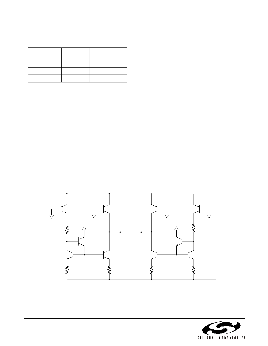
4.4.4. Transistor Power Equations
(Using Discrete Transistors)
When using the Si3232 along with discrete bipolar
transistors, it is possible to control the total power of the
solution by regulating the power in each discrete
transistor individually. Figure 11 illustrates the basic
transistor-based linefeed circuit for one channel. The
power dissipation of each external transistor is
estimated based on the A/D sample values. The
approximate power equations for each external BJT are
as follows:
P
Q1
V
CE1
x I
Q1
(|V
TIP
| + 0.75 V) x (I
Q1
)
P
Q2
V
CE2
x I
Q2
(|V
RING
| + 0.75 V) x (I
Q2
)
P
Q3
V
CE3
x I
Q3
(|V
BAT
| � R7 x I
Q5
) x (I
Q3
)
P
Q4
V
CE4
x I
Q4
(|V
BAT
| � R6 x I
Q6
) x (I
Q4
)
P
Q5
V
CE5
x I
Q5
(|V
BAT
| � |V
RING
|
� R7 x I
Q5
) x (I
Q5
)
P
Q6
V
CE6
x I
Q6
(|V
BAT
| � |V
TIP
|
� R6 x I
Q6
) x (I
Q6
)
Figure 11. Discrete Linefeed Circuit for Power Monitoring
Table 15. Register Values for CM Calibration
(600
Impedance Synthesis)
Register
Name
Register
Location
(decimal)
Register
Value
(hexadecimal)
ZRS
33
0x5
ZZ
34
0x1
Q2
Q5
R7
IRINGP
Q9
R7*gain
IRINGN
Q3
RING
Q1
Q6
R6
ITIPP
Q10
R6*gain
ITIPN
Q4
TIP
VBAT
RBQ6
RBQ5
Q8
Q7
82.5
1.74k
82.5
1.74k

Si3232
Preliminary Rev. 0.96
27
The maximum power threshold for each device is
software-programmable and should be set based on the
characteristics of the transistor package, PCB design,
and available airflow. If the peak power exceeds the
programmed threshold for any device, the power alarm
bit is set for that device. Each external bipolar has its
own register bit (PQ1S�PQ6S bits of the IRQVEC3
register) which goes high on a rising edge of the
comparator output and remains high until the user
clears it. Each transistor power alarm bit is also
maskable by setting the PQ1E�PQ6E bits in the
IRQEN3 register.
4.4.5. Si3200 Power Calculation
When using the Si3200, it is also possible to detect the
thermal conditions of the linefeed circuit by calculating
the total power dissipated within the Si3200. This case
is similar to the Transistor Power Equations case, with
the exception that the total power from all transistor
devices is dissipated within the same package
enclosure and the total power result is placed in the
PSUM RAM location. The power calculation is derived
using the following set of equations:
P
Q1
(|V
TIP
| + 0.75 V) x I
Q1
P
Q2
(|V
RING
| + 0.75 V) x I
Q2
P
Q3
(|V
BAT
|+ 0.75 V) x I
Q3
P
Q4
(|V
BAT
| + 0.75 V) x I
Q4
P
Q5
(|V
BAT
| � |V
RING
|) x I
Q5
P
Q6
(|V
BAT
| � |V
TIP
|) x I
Q6
PSUM = total dissipated power = P
Q1
+ P
Q2
+ P
Q3
+
P
Q4
+ P
Q5
+ P
Q6
Note: The Si3200 THERM pin must be connected to the
THERM a/b pin of the Si3232 in order for the Si3200
power calculation to work correctly.
4.4.6. Power Filter and Alarms
The power calculated during each A/D sample period
must be filtered before being compared to a user-
programmable maximum-power threshold. A simple
digital low-pass filter is used to approximate the
transient thermal behavior of the package, with the
output of the filter representing the effective peak power
within the package or, equivalently, the peak junction
temperature.
For Q1, Q2, Q3, Q4 in SOT23 and Q5, and Q6 in
SOT223 packages, the settings for thermal low-pass
filter poles and power threshold settings are (for an
ambient temperature of 70 �C) calculated as follows:
Suppose that the thermal time constant of the package
is
thermal
. The decimal values of RAM locations
PLPF12, PLPF34, and PLPF56 are given by rounding
to the next integer the value given by the following
equation:
where 4096 is the maximum value of the 12-bit plus
sign RAM locations, PLPF12, PLPF34, and PLPF56,
and 800 is the power calculation clock rate in Hz. The
equation is an excellent approximation of the exact
equation for
thermal
= 1.25 ms ... 5.12 s. With the
above equations in mind, example values of the RAM
locations, PTH12, PTH34, PTH56, PLPF12, PLPF34,
and PLPF56 follow:
PTH12 = power threshold for Q1, Q2 = 0.3 W (0x25A)
PTH34 = power threshold for Q3, Q4 = 0.22 W
(0x1BSE)
PTH56 = power threshold for Q5, Q6 = 1 W (0x7D8)
PLPF12 = Q1/Q2 Thermal LPF pole = 0x0012 (for SOT-
89 package)
PLPF34 = Q3/Q4 Thermal LPF pole = 0x008C (for
SOT-23 package)
PLPF56 = Q5/Q6 thermal LPF pole = 0x000E (for SOT-
223 package)
When Si3200 is used, the thermal filtering needs to be
performed on the total power reflected in the PSUM
RAM location. When the filter output exceeds the total
power threshold, an interrupt is issued. The PTH12
RAM location is used to preset the total power threshold
for the Si3200, and the PLPF12 RAM location is used to
preset the thermal low-pass filter pole.
When the THERM pin is connected from the Si3232 to
the Si3200 (indicating the presence of an Si3200), the
resolution of the PTH12 and PSUM RAM locations is
modified from 498
�W/LSB to 1059.6 �W/LSB.
Additionally, the
THERMAL
value must be modified to
accommodate the Si3200.
THERMAL
for the Si3200 is
typically 0.7 s assuming the exposed pad is connected
to the recommended ground plane as stated in Table 1.
THERMAL
decreases if the PCB layout does not provide
sufficient thermal conduction. See "AN58: Si3220/
Si3225 Programmer's Guide" for details.
Example calculations for PTH12 and PLPF12 in Si3200
mode are shown below:
PTH12 = Si3200 power threshold = 1 W (0x3B0)
PLPF12 = Si3200 thermal LPF pole = 2 (0x0010)
4.4.7. Automatic State Change Based on Power
Alarm
If any of the following situations occurs, the device
automatically transitions to the OPEN state:
Any of the transistor power alarm thresholds is
exceeded (in the case of the discrete transistor
circuit).
PLPFxx (decimal value)
4096
800
thermal
�
------------------------------------ 2
3
�
=

Si3232
28
Preliminary Rev. 0.96
The total power threshold is exceeded (when using
the power calculator method along with the Si3200).
To provide optimal reliability, the device automatically
transitions into the open state until the user changes the
state manually, independent of whether or not the power
alarm interrupt has been masked. The PQ1E to PQ6E
bits of the IRQEN3 register are used to enable the
interrupts for each transistor power alarm, and the
PQ1S to PQ6S bits of the IRQVEC3 register are set
when a power alarm is triggered in the respective
transistor. When using the Si3200, the PQ1E bit is used
to enable the power alarm interrupt, and the PQ1S bit is
set when a Si3200 power alarm is triggered.
4.4.8. Power Dissipation Considerations
The Si3232 relies on the Si3200 to power the line from
the battery supply. The PCB layout and enclosure
conditions should be designed to allow sufficient
thermal dissipation out of the Si3200, and a
programmable power alarm threshold ensures product
safety under all operating conditions. See "4.4.3. Power
Monitoring and Power Fault Detection" for more details
on power alarm considerations. The Si3200's thermally-
enhanced SOIC-16 package offers an exposed pad that
improves thermal dissipation out of the package when
soldered to a topside PCB pad connected to inner
power planes. Using appropriate layout practices, the
Si3200 can provide thermal performance of 55 �C/W.
The exposed path should be connected to a low-
impedance ground plane via a topside PCB pad directly
under the part. See package outlines for PCB pad
dimensions. In addition, an opposite-side PCB pad with
multiple vias connecting it to the topside pad directly
under the exposed pad further improves the overall
thermal performance of the system. Refer to "AN55:
Dual ProSLICTM User Guide" or the Si3232 evaluation
board data sheet for layout guidelines for optimal
thermal dissipation.
Table 16. Register and RAM Locations used for Power Monitoring and Power Fault Detection
Parameter
Location
Register/RAM
Bits
Measurement
Range
Resolution
Si3200 Power Output Monitor
PSUM
PSUM[15:0]
0 to 34.72 W
1059.6
�W
Si3200 Power Alarm Interrupt Pending
IRQVEC3
PQ1S
N/A
N/A
Si3200 Power Alarm Interrupt Enable
IRQEN3
PQ1E
N/A
N/A
Q1/Q2 Power Alarm Threshold (discrete)
Q1/Q2 Power Alarm Threshold (Si3200)
PTH12
PTH12[15:0]
0 to 16.319 W
0 to 34.72 W
498
�W
1059.6
�W
Q3/Q4 Power Alarm Threshold
PTH34
PTH34[15:0]
0 to 1.03 W
31.4
�W
Q5/Q6 Power Alarm Threshold
PTH56
PTH56[15:0]
0 to 16.319 W
498
�W
Q1/Q2 Thermal LPF Pole
PLPF12
PLPF12[15:3]
See "4.4.6. Power Filter and
Alarms"
Q3/Q4 Thermal LPF Pole
PLPF34
PLPF34[15:3]
See "4.4.6. Power Filter and
Alarms"
Q5/Q6 Thermal LPF Pole
PLPF56
PLPF56[15:3]
See "4.4.6. Power Filter and
Alarms"
Q1�Q6 Power Alarm Interrupt Pending
IRQVEC3
TBD
N/A
Q71�Q6 Power Alarm Interrupt Enable
IRQEN3
TBD
N/A

Si3232
Preliminary Rev. 0.96
29
4.5. Automatic Dual Battery Switching
The Si3232 and Si3200 provide the ability to switch
between several user-provided battery supplies to aid
thermal management. This method is required during
the ringing to off-hook and on-hook to off-hook state
transitions.
During the on-hook operating state, the Si3232 must
operate from the ringing battery supply in order to
quickly provide the desired ringing signal when
required. Once an off-hook condition has been
detected, the Si3232 must transition to the lower battery
supply (typically �24 V, in order to reduce power
dissipation during the active state). The low current
consumed by the Si3232 during the on-hook state
results in very little power dissipation while being
powered from the ringing battery supply, which can
have an amplitude as high as 100 V depending on the
desired ringing amplitude.
The BATSEL pins serve to switch between the two
battery voltages based on the operating state and the
TIP-RING voltage. Figure 12 illustrates the chip
connections required to implement an automatic dual
battery switching scheme. When BATSEL is pulled low,
the desired channel is powered from the V
BLO
supply.
When BATSEL is pulled high, the V
BHI
source will
supply power to the desired channel.
The BATSEL pins for both channels are controlled using
the BATSEL bit of the RLYCON register and should be
programmed to automatically switch to the lower battery
supply (V
BLO
) whenever an off-hook condition is
sensed.
Two thresholds are provided to enable battery switching
with hysteresis. The BATHTH RAM location specifies
the threshold at which the Si3232 will switch from the
low battery, V
BLO
, to the high battery, V
BHI
, due to an
off-hook to on-hook transition. The BATLTH RAM
location specifies the threshold at which the Si3232 will
switch from V
BHI
to V
BLO
due to a transition from the on-
hook or ringing state to the off-hook state or because
the overhead during active off-hook mode is sufficient to
feed the subscriber loop using a lower battery voltage.
The low-pass filter coefficient is calculated using the
equation below and is entered into the BATLPF RAM
location.
BATLPF = [(2
f x 4096)/800] x 2
3
Where f = the desired cutoff frequency of the filter
The programmable range of the filter is from 0 (blocks
all signals) to 4000h (unfiltered). A typical value of 10
(0A10h) is sufficient to filter out any unwanted ac
artifacts while allowing the dc information to pass
through the filter.
Table 17 provides the register and RAM locations used
for programming the battery switching functions.
Table 17. Register and RAM Locations used for Battery Switching
Parameter
Register/RAM
Mnemonic
Register/RAM
Bits
Programmable
Range
Resolution
(LSB Size)
High Battery Detect Threshold
BATHTH
BATHTH[14:0]
0 to 160.173 V
*
628 mV
(4.907 mV)
Low Battery Detect Threshold
BATLTH
BATLTH[14:0]
0 to 160.173 V
*
628 mV
(4.907 mV)
Ringing Battery Switch
RLYCON
GPO
Toggle
N/A
Battery Select Indicator
RLYCON
BSEL
Toggle
N/A
Battery Switching LPF
BATLPF
BATLPF[15:3]
0 to 4000
N/A
*Note: The usable range for BATHTH and BATLTH is limited to the
V
BHI
voltage.

Si3232
30
Preliminary Rev. 0.96
Figure 12. External Battery Switching Using the Si3232 and Si3200
When generating a high-voltage ringing amplitude using the Si3220, the power dissipated during the OHT state
typically increases due to operating from the ringing battery supply in this mode. To reduce power, the Si3232/
Si3200 chipset provides the ability to accommodate up to three separate battery supplies by implementing a
secondary battery switch using a few low-cost external components as illustrated in Figure 13. The Si3232's
BATSEL pin is used to switch between the V
BHI
(typically �48 V) and V
BLO
(typically �24 V) rails using the switch
internal to the Si3200. The Si3232's GPO pin is used along with the external transistor circuit to switch the V
BRING
rail (the ringing voltage battery rail) onto the Si3200's VBAT pin when ringing is enabled. The GPO signal is driven
automatically by the ringing cadence provided that the RRAIL bit of the RLYCON register is set to 1 (signifying that
a third battery rail is present).
Si3232
BATSEL
Linefeed
Circuitry
VBATL
V
BLO
V
BHI
Si3200
BATSEL
Battery
Sensing
Circuit
Battery
Select
Control
806 k
SVBAT
40.2 k
Battery
Logic
Control
VBAT
VBATH

Si3232
Preliminary Rev. 0.96
31
Figure 13. Three-Battery Switching with Si3232
Si3232
Si3200
SVBAT
BAT
SEL
GP
O
VBAT
VBATH
VBATL
BATSEL
806 k
0.1
�F
0.1
�F
D1
IN4003
R101
Q1
CXT5401
Q2
CXT5551
R102
10 k
R103
402 k
V
BRING
V
BLO
R5
V
BHI
R9
40.2 k

Si3232
32
Preliminary Rev. 0.96
4.5.1. Loop Closure Detection
Loop closure detection is required to accurately signal a
terminal device going off-hook during the Active or On-
Hook Transmission linefeed states (forward or reverse
polarity). The functional blocks required to implement a
loop closure detector are shown in Figure 14, and the
register set for detecting a loop closure event is
provided in Table 19. The primary input to the system is
the Loop Current Sense value provided by the voltage/
current/power monitoring circuitry and reported in the
ILOOP RAM address. The loop current (I
LOOP
) is
computed by the ISP using the equations shown below.
Refer to Figure 11 on page 26 for the discrete bipolar
transistor references used in the equation below (Q1,
Q2, Q5 and Q6 � note that the Si3200 has
corresponding MOS transistors). The same I
LOOP
equation applies to the discrete bipolar linefeed as well
as the Si3200 linefeed device. The following equation is
conditioned by the CMH status bit in register LCRRTP
and by the linefeed state as indicated by the LFS field in
the LINEFEED register.
If the CMHITH (RAM 36) threshold is exceeded, the
CMH bit is 1, and I
Q1
is forced to zero in the
FORWARD-ACTIVE and TIP-OPEN states, or I
Q2
is
forced to zero in the REVERSE-ACTIVE and RING-
OPEN states. The other currents in the equation are
allowed to contribute normally to the I
LOOP
value.
The conditioning due to the CMH bit (LCRRTP Register)
and LFS field (LINEFEED Register) states can be
summarized as follows:
IQ1 = 0 if (CMH = 1 AND (LFS = 1 OR LFS = 3))
IQ2 = 0 if (CMH = 1 AND (LFS = 5 OR LFS = 7))
The output of the Input Signal Processor is the input to a
programmable digital low-pass filter, which can be used
to remove unwanted ac signal components before
threshold detection.
The low-pass filter coefficient is calculated using the
following equation and is entered into the LCRLPF RAM
location.
LCRLPF = [(2
f x 4096)/800] x 2
3
Where f is the desired cutoff frequency of the filter.
The programmable range of the filter is from 0h (blocks
all signals) to 4000h (unfiltered). A typical value of 10
(0A10h) is sufficient to filter out any unwanted ac
artifacts while allowing the dc information to pass
through the filter.
The output of the low-pass filter is compared to a
programmable threshold, LCROFFHK. Hysteresis is
enabled by programming a second threshold,
LCRONHK, to detect the loop going to an OPEN or on-
hook state. The threshold comparator output feeds a
programmable debounce filter. The output of the
debounce filter remains in its present state unless the
input remains in the opposite state for the entire period
of time programmed by the loop-closure debounce
interval, LCRDBI. There is also a loop-closure mask
interval, LCRMASK, that is used to mask transitions
caused when an internal ringing burst (no dc offset)
ends in the presence of a high REN load. If the
debounce interval has been satisfied, the LCR bit will be
set to indicate that a valid loop closure has occurred.
Table 18. 3-Battery Switching Components
Component
Value
Comments
D1
200 V, 200 mA
IN4003 or similar
Q1
100 V PNP
CXT5401 or similar
Q2
100 V NPN
CXT5551 or similar
R101
1/10 W, �5%
2.4 k
for V
DD
= 3.3 V
3.9 k
for V
DD
= 5 V
R102
10 k
, 1/10 W, �5%
R103
402 k
, 1/10 W, �1%
I
loop
I
Q1
I
Q6
�
I
Q5
I
Q2
in TIP-OPEN or RING-OPEN
I
Q1
I
Q6
�
I
Q5
I
Q2
�
+
2
---------------------------------------------------- in all other states
=
�
+
=
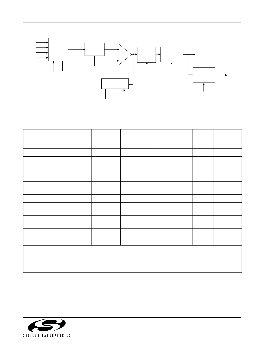
Si3232
Preliminary Rev. 0.96
33
Figure 14. Loop Closure Detection Circuitry
Table 19. Register and RAM Locations used for Loop Closure Detection
Parameter
Register/
RAM
Mnemonic
Register/RAM
Bits
Programmable
Range
LSB
Size
Resolution
Loop Closure Interrupt Pending
IRQVEC2
LOOPS
Yes/No
N/A
N/A
Loop Closure Interrupt Enable
IRQEN2
LOOPE
Yes/No
N/A
N/A
Linefeed Shadow
LINEFEED
LFS[2:0]
Monitor only
N/A
N/A
Loop Closure Detect Status
LCRRTP
LCR
Monitor only
N/A
N/A
Loop Closure Detect Debounce
Interval
LCRDBI
LCRDBI[15:0]
0 to 40.96 s
1.25 ms
1.25 ms
Loop Current Sense
ILOOP
ILOOP[15:0]
0 to 101.09 mA
3.097
�A
500
�A
1
Loop Closure Threshold (on-hook to
off-hook)
LCROFFHK
LCROFFHK[15:0]
0 to 101.09 mA
2
3.097
�A
396.4
�A
Loop Closure Threshold (off-hook to
on-hook)
LCRONHK
LCRONHK[15:0]
0 to 101.09 mA
2
3.097
�A
396.4
�A
Loop Closure Filter Coefficient
LCRLPF
LCRLPF[15:3]
0 to 4000h
N/A
N/A
Loop Closure Mask Interval
LCRMASK
LCRMASK[15:0]
0 to 40.96 s
1.25 ms
1.25 ms
Notes:
1. I
LOOP
is a calculated value based on measured I
Q1
�I
Q4
currents. The resulting effective resolution is approximately
500
�A.
2. The usable range for LCRONHK and LCROFFHK is limited to 61 mA. Entering a value >61 mA disables threshold
detection.
I
Q1
LFS
LCRLPF
LCROFFHK
Input
Signal
Processor
Digital
LPF
Loop Closure
Threshold
Debounce
Filter
+
�
LCR
LCRONHK
LOOPS
LOOPE
Interrupt
Logic
LCRDBI
Loop
Closure
Mask
LCRMASK
I
Q2
I
Q5
I
Q6
CMH
I
LOOP

Si3232
34
Preliminary Rev. 0.96
4.5.2. Ground Key Detection
Ground key detection detects an alerting signal from the
terminal equipment during the tip open or ring open
linefeed states. The functional blocks required to
implement a ground key detector are shown in
Figure 15, and the register set for detecting a ground
key event is provided in Table 22 on page 36. The
primary input to the system is the longitudinal current
sense value provided by the voltage/current/power
monitoring circuitry and reported in the ILONG RAM
address. The I
LONG
value is produced in the ISP
provided the LFS bits in the linefeed register indicate
the device is in the tip open or ring open state.
The longitudinal current (I
LONG
) is computed as shown
in the following equation. Refer to Figure 11 on page 26
for the transistor references used in the equation (Q1,
Q2, Q5 and Q6 � note that the Si3200 has
corresponding MOS transistors). The same I
LONG
equation applies to the discrete bipolar linefeed as well
as the Si3200 linefeed device.
The output of the ISP (I
LONG
) is the input to a
programmable, digital low-pass filter, which removes
unwanted ac signal components before threshold
detection.
The low-pass filter coefficient is calculated using the
following equation and is entered into the LONGLPF
RAM location:
Where f = the desired cutoff frequency of the filter.
The programmable range of the filter is from 0h (blocks
all signals) to 4000h (unfiltered). A typical value of 10
(0A10h) is sufficient to filter out any unwanted ac
artifacts while allowing the dc information to pass
through the filter.
The output of the low-pass filter is compared to the
programmable threshold, LONGHITH. Hysteresis is
enabled by programming a second threshold,
LONGLOTH, to detect when the ground key is released.
The threshold comparator output feeds a programmable
debounce filter.
The output of the debounce filter remains in its present
state unless the input remains in the opposite state for
the entire period of time programmed by the loop
closure debounce interval, LONGDBI. If the debounce
interval is satisfied, the LONGHI bit is set to indicate
that a valid ground key event has occurred.
When the Si3220/25 detects a ground key event, the
linefeed automatically transitions from the TIP-OPEN
(or RING-OPEN) state to the FORWARD-ACTIVE (or
REVERSE-ACTIVE) state. However, this automatic
state transition is triggered by the LCR bit becoming
active (i.e., =1), and not by the LONGHI bit.
While I
LONG
is used to generate the LONGHI status bit,
a transition from TIP-OPEN to the FORWARD-ACTIVE
state (or from the RING-OPEN to the REVERSE-
ACTIVE state) occurs when the RING terminal (or TIP
terminal) is grounded and is based on the LCR bit and
implicitly on exceeding the LCROFFHK threshold.
As an example of ground key detection, suppose that
the Si3220/25 has been programmed with the current
values shown in Table 20.
With the settings of Table 20, the behavior of I
LOOP
,
I
LONG
, LCR, LONGHI, and CMHIGH is as shown in
Table 21. The entries under "Loop State" indicate the
condition of the loop, as determined by the equipment
terminating the loop. The entries under "LINEFEED
Setting" indicate the state initially selected by the host
CPU (e.g., TIP-OPEN) and the automatic transition to
the FORWARD-ACTIVE state due to a ground key
event (when RING is connected to GND). The transition
from state #2 to state #3 in Table 21 is the automatic
transition from TIP-OPEN to FWD-ACTIVE in response
to LCR = 1.
I
LONG
I
Q1
I
Q6
�
I
Q5
�
I
Q2
+
2
----------------------------------------------------
=
LONGLPF
2
f 4096
�
(
)
800
---------------------------------
2
3
�
=
Table 20. Settings for Ground Key Example
ILIM
21 mA
LCROFFHK
14 mA
LCRONHK
10 mA
LONGHITH
7 mA
LONGLOTH
5 mA

Si3232
Preliminary Rev. 0.96
35
Figure 15. Ground Key Detection Circuitry
Table 21. State Transitions During Ground Key Detection
#
Loop
State
LINEFEED
State
I
LOOP
(mA) I
LONG
(mA)
LCR
LONGHI
CMHIGH
1
LOOP OPEN
LFS = 3
(TIP-OPEN)
0
0
0
0
0
2
RING-GND
LFS = 3
(TIP-OPEN)
22
�11
1
1
0
3
RING-GND
LFS = 1
(FWD-ACTIVE)
22
�11
1
1
1
4
LOOP CLOSURE
LFS = 1
(FWD-ACTIVE)
21
0
1
0
0
5
LOOP OPEN
LFS = 1
(FWD-ACTIVE)
0
0
0
0
0
I
Q1
LFS
LONGLPF
LONGHITH
Input
Signal
Processor
Digital
LPF
Ground Key
Threshold
Debounce
Filter
+
�
LONGHI
LONGLOTH
LONGS
LONGE
Interrupt
Logic
LONGDBI
I
Q2
I
Q5
I
Q6
I
LONG

Si3232
36
Preliminary Rev. 0.96
Table 22. Register and RAM Locations used for Ground Key Detection
Parameter
Register/
RAM
Mnemonic
Register/RAM
Bits
Programmable
Range
LSB Size
Resolutio
n
Ground Key Interrupt Pend-
ing
IRQVEC2
LONGS
Yes/No
N/A
N/A
Ground Key Interrupt Enable
IRQEN2
LONGE
Yes/No
N/A
N/A
Linefeed Shadow
LINEFEED
LFS[2:0]
Monitor only
N/A
N/A
Ground Key Detect Status
LCRRTP
LONGHI
Monitor only
N/A
N/A
Ground Key Detect
Debounce Interval
LONGDBI
LONGDBI[15:0]
0 to 40.96 s
1.25 ms
1.25 ms
Longitudinal Current Sense
ILONG
ILONG[15:0]
Monitor only
See
Table 14
Ground Key Threshold (high)
LONGHITH
LONGHITH[15:0]
0 to 101.09 mA
*
3.097 �A
396.4 �A
Ground Key Threshold (low)
LONGLOTH
LON-
GLOTH[15:0]
0 to 101.09 mA
*
3.097 �A
396.4 �A
Ground Key Filter Coefficient
LONGLPF
LONGLPF[15:3]
0 to 4000h
N/A
N/A
Note: The usable range for LONGHITH and LONGLOTH is limited to 16 mA. Setting a value >16 mA will disable threshold
detection

Si3232
Preliminary Rev. 0.96
37
4.6. Ringing Generation
The Si3232 is designed to provide a balanced ringing
waveform with or without dc offset. The ringing
frequency, cadence, waveshape, and dc offset are all
register-programmable.
Using a balanced ringing scheme, the ringing signal is
applied to both the TIP and the RING lines using ringing
waveforms that are 180� out of phase with each other.
The resulting ringing signal seen across TIP-RING is
twice the amplitude of the ringing waveform on either
the TIP or the RING line, which allows the ringing
circuitry to withstand only half the total ringing amplitude
seen across TIP-RING.
Figure 16. Balanced Ringing Waveform and
Components
The purpose of an internal ringing scheme is to provide
>40 V
rms
into a 5 REN load at the terminal equipment
using a user-provided ringing battery supply. The
specific ringing supply voltage required depends on the
ringing voltage desired.
The ringing amplitude at the terminal equipment
depends on the loop impedance as well as the load
impedance in REN. The following equation can be used
to determine the TIP-RING ringing amplitude required
for a specific load and loop condition.
Figure 17. Simplified Loop Circuit During
Ringing
where
When ringing longer loop lengths, adding a dc offset
voltage is necessary to reliably detect a ring trip
condition (off-hook phone). Adding dc offset to the
ringing signal decreases the maximum possible ringing
amplitude. Adding significant dc offset also increases
the power dissipation in the Si3200 and may require
additional airflow or a modified PCB layout to maintain
acceptable operating temperatures. The Si3232
automatically applies and removes the ringing signal
during V
OC
-crossing periods to reduce noise and
crosstalk to adjacent lines. Table 23 provides a list of
registers required for internal ringing generation.
RING
TIP
V
RING
V
TIP
SLIC
V
OFF
GND
V
TIP
V
RING
V
BATH
V
PK
V
OV
V
CM
V
OFF
R
LOOP
V
RING
R
LOAD
V
TERM
+
�
R
OUT
V
TERM
V
RING
R
LOAD
R
LOAD
R
LOOP
R
OUT
+
+
----------------------------------------------------------------
�
=
R
LOOP
0.09
per foot for 26 AWG wire
=
R
OUT
320
=
R
LOAD
7000
#REN
--------------------
=

Si3232
38
Preliminary Rev. 0.96
4.6.1. Internal Sinusoidal Ringing
A sinusoidal ringing waveform is generated by using an
on-chip digital tone generator. The tone generator used
to generate ringing tones is a two-pole resonator with a
programmable frequency and amplitude. Since ringing
frequencies are low compared to the audio band
signaling frequencies, the sinusoid is generated at a
1 kHz rate. The ringing generator is programmed via the
RINGFREQ, RINGAMP, and RINGPHAS RAM
locations. The equations are as follows:
For example, to generate a 60 V
rms
(87 V
PK
), 20 Hz
ringing signal, the equations are as follows:
Table 23. Register and RAM Locations used for Ringing Generation
Parameter
Register/RAM
Mnemonic
Register/RAM
Bits
Programmable
Range
Resolution
(LSB Size)
Ringing Waveform
RINGCON
TRAP
Sinusoid/Trapezoid
N/A
Ringing Active Timer Enable
RINGCON
TAEN
Enabled/Disabled
N/A
Ringing Inactive Timer Enable
RINGCON
TIEN
Enabled/Disabled
N/A
Ringing Oscillator Enable Monitor
RINGCON
RINGEN
Enabled/Disabled
N/A
Ringing Oscillator Active Timer
RINGTALO/
RINGTAHI
RINGTA[15:0]
0 to 8.19 s
125 ms
Ringing Oscillator Inactive Timer
RINGTILO/
RINGTIHI
RINGTI[15:0]
0 to 8.19 s
125 ms
Linefeed Control (Initiates Ringing
State)
LINEFEED
LF[2:0]
000 to 111
N/A
On-Hook Line Voltage
VOC
VOC[15:0]
0 to 63.3 V
1.005 V
(4.907 mV)
Ringing Voltage Offset
RINGOF
RINGOF[15:0]
0 to 63.3 V
1.005 V
(4.907 mV)
Ringing Frequency
RINGFRHI/
RINGFRLO
RINGFRHI[14:3]/
RINGFRLO[14:3]
4 to 100 Hz
Ringing Amplitude
RINGAMP
RINGAMP[15:0]
0 to 160.173 V
628 mV
(4.907 mV)
Ringing Initial Phase
Sinusoidal
Trapezoid
RINGPHAS
RINGPHAS[15:0]
N/A
0 to 1.024 s
N/A
31.25
�s
Ringing Overhead Voltage
VOVRING
VOVRING[15:0]
0 to 63.3 V
1.005 V
(4.907 mV)
Ringing Speedup Timer
SPEEDUPR
SPEEDUPR[15:0]
0 to 40.96 s
1.25 ms
coeff
2
f
1000 Hz
-----------------------
cos
=
RINGFREQ
coeff 2
23
�
=
RINGAMP
1
4
--- 1 coeff
�
1 coeff
+
------------------------
2
15
(
)
�
Desired V
PK
160.173 V
-----------------------------------
�
=
RINGPHAS
0
=
coeff
2
20
1000 Hz
-----------------------
.99211
=
cos
=
RINGFREQ
.99211
2
23
(
)
�
8322461
0x7EFD9D
=
=
=

Si3232
Preliminary Rev. 0.96
39
In addition to the variable frequency and amplitude,
there is a selectable dc offset (V
OFF
) that can be added
to the waveform. The dc offset is defined in the RINGOF
RAM location. The ringing generator has two timers
which allow on/off cadence settings up to 8 s on/8 s off.
In addition to controlling ringing cadence, these timers
control the transition into and out of the ringing state.
To initiate ringing, the user must program the
RINGFREQ, RINGAMP, and RINGPHAS RAM
addresses as well as the RINGTA, and RINGTI
registers, and select the ringing waveshape and dc
offset. Once this is done, the TAEN and TIEN bits are
set as desired. Ringing state is invoked by a write to the
linefeed register. At the expiration of RINGTA, the
Si3232 turns off the ringing waveform and goes to the
on-hook transmission state. At the expiration of RINGTI,
ringing is initiated again. This process continues as long
as the two timers are enabled and the linefeed register
remains in the ringing state.
4.6.2. Internal Trapezoidal Ringing
In addition to the traditional sinusoidal ringing
waveform, the Si3232 can generate a trapezoidal
ringing waveform similar to the one illustrated in
Figure 19. The RINGFREQ, RINGAMP, and
RINGPHAS RAM locations are used for programming
the ringing wave shape as follows:
RINGPHAS = 4 x Period x 8000
RINGAMP = (Desired V/160.8 V) x (2
15
)
RINGFREQ = (2 x RINGAMP) / (t
RISE
x 8000)
RINGFREQ is a value that is added or subtracted from
the waveform to ramp the signal up or down in a linear
fashion. This value is a function of rise time, period, and
amplitude, where rise time and period are related
through the following equation for the crest factor of a
trapezoidal waveform.
where
So, for a 90 V
PK
, 20 Hz trapezoidal waveform with a
crest factor of 1.3, the period is 0.05 s, and the rise time
requirement is 0.015 s.
RINGPHAS = 4 x 0.05 x 8000 = 1600 (0x0640)
RINGAMP = 90/160.8 x (2
15
) = 18340 (0x47A5)
RINGFREQ = (2 x RINGAMP) (0.0153 x 8000) =
300 (0x012C)
The time registers and interrupts described in the
sinusoidal ring description also apply to the trapezoidal
ring waveform.
4.7. Internal Unbalanced Ringing
The Si3232 also provides the ability to generate a
traditional battery-backed unbalanced ringing waveform
for ringing terminating devices that require a high dc
content or for use in ground-start systems that cannot
tolerate a ringing waveform on both the TIP and RING
leads. The unbalanced ringing scheme applies the
ringing signal to the RING lead; the TIP lead remains at
the programmed VCM voltage that is very close to
ground. A programmable dc offset can be preset to
provide dc current for ring trip detection. Figure 18
illustrates the internal unbalanced ringing waveform.
Figure 18. Internal Unbalanced Ringing
To enable unbalanced ringing, set the RINGUNB bit of
the RINGCON register. As is the case with internal
balanced ringing, the unbalanced ringing waveform is
generated by using the on-chip ringing tone generator.
The tone generator used to generate ringing tones is a
two-pole resonator with programmable frequency and
amplitude. Since ringing frequencies are low compared
to the audio band signaling frequencies, the ringing
waveform is generated at a 1 kHz rate.
The ringing generator is programmed via the RINGAMP,
RINGFREQ, and RINGPHAS registers. The RINGOF
register is used to set the dc offset position around
RINGAMP
1
4
--- .00789
1.99211
---------------------
2
15
(
)
�
85
160.173
---------------------
�
273
0x111
=
=
=
t
RISE
3
4
---T 1
1
CF
2
-----------
�
=
T
Period
1
f
RING
--------------
CF
desired crest factor
=
=
=
RING
TIP
V
RING
Si3232
DC Offset
GND
V
TIP
V
RING
V
BATR
-80V
V
OVRING
V
CM
DC Offset
V
OFF

Si3232
40
Preliminary Rev. 0.96
which the RING lead oscillates. The dc offset is set at a
dc point equal to V
CM
� (�80 V + V
OFF
), where V
OFF
is
the value that is input into the RINGOF RAM location.
Positive V
OFF
values cause the dc offset point to move
closer to ground (lower dc offset), and negative V
OFF
values have the opposite effect. The dc offset can be
set to any value; however, the ringing signal is clipped
digitally if the dc offset is set to a value that is less than
half the ringing amplitude. In general, the following
equation must hold true to ensure the battery voltage is
sufficient to provide the desired ringing amplitude:
|V
BATR
| > |V
RING,PK
+ (�80 V + V
OFF
) + V
OVRING
|
It is possible to create reverse polarity unbalanced
ringing waveforms (the TIP lead oscillates while the
RING lead stays constant) by setting the UNBPOLR bit
of the RINGCON register. In this mode, the polarity of
V
OFF
must also be reversed (in normal ringing polarity,
V
OFF
is subtracted from �80 V, and in reverse polarity,
ringing V
OFF
is added to �80 V).
4.7.1. Ringing Coefficients
The ringing coefficients are calculated in decimal for
sinusoidal and trapezoidal waveforms. The RINGPHAS
and RINGAMP hex values are decimal-to-hex
conversions in 16-bit, 2's complement representations
for their respective RAM locations.
To obtain sinusoidal RINGFREQ RAM values, the
RINGFREQ decimal number is converted to a 24-bit 2's
complement value. The lower 12 bits are placed in
RINGFRLO bits 14:3. RINGFRLO bits 15 and 2:0 are
cleared to 0. The upper 12 bits are set in a similar
manner in RINGFRHI, bits 13:3. RINGFRHI bit 14 is the
sign bit and RINGFRHI bits 2:0 are cleared to 0.
For example, the register values for
RINGFREQ = 0x7EFD9D are as follows:
RINGFRHI = 0x3F78
RINGFRLO = 0x6CE8
To obtain trapezoidal RINGFREQ RAM values, the
RINGFREQ decimal number is converted to an 8-bit, 2's
complement value. This value is loaded into RINGFRHI.
RINGFRLO is not used.
Figure 19. Trapezoidal Ringing Waveform
4.7.2. Ringing DC Offset Voltage
A dc offset voltage can be added to the Si3232's ac
ringing waveform by programming the RINGOF RAM
address to the appropriate setting. The value of
RINGOF is calculated as follows:
4.7.3. Linefeed Overhead Voltage Considerations
During Ringing
The ringing mode output impedance allows ringing
operation without overhead voltage modification
(V
OVR
= OV). If an offset of the ringing signal from the
RING lead is desired, V
OVR
can be used for this
purpose.
4.7.4. Ringing Power Considerations
The total power consumption of the Si3232/Si3200
chipset using internal ringing generation is dependent
on the V
DD
supply voltage, the desired ringing
amplitude, the total loop impedance, and the ac load
impedance (number of REN). The following equations
can be used to approximate the total current required
for each channel during ringing mode.
Where:
time
V
OFF
T=1/freq
t
RISE
V
TIP-RING
RINGOF
V
OFF
160.8
--------------- 2
15
�
=
I
DD,AVE
V
RING,PK
Z
LOOP
----------------------- 2
--- I
DD,OH
+
�
=
I
BAT,AVE
V
RING,PK
Z
LOOP
----------------------- 2
---
�
=
V
RING,PK
V
RING,RMS
2
�
=
Z
LOOP
R
LOOP
R
LOAD
R
OUT
+
+
=
R
LOAD
7000
REN
------------- (for North America)
=

Si3232
Preliminary Rev. 0.96
41
4.8. Ring Trip Detection
A ring trip event signals that the terminal equipment has
transitioned to an off-hook condition after ringing has
commenced, thus ensuring that the ringing signal is
removed before normal speech begins. The Si3232 is
designed to implement either an ac- or dc-based
internal ring trip detection scheme or a combination of
both schemes. This allows system-design flexibility for
addressing varying loop lengths of different
applications. An ac ring trip detection scheme cannot
reliably detect an off-hook condition when sourcing
longer loop lengths, as the 20 Hz ac impedance of an
off-hook long loop is indistinguishable from a heavily-
loaded (5 REN) short loop in the on-hook state.
Because of this situation, a dc ring trip detection
scheme is required when sourcing longer loop lengths.
The Si3232 can implement either an ac- or dc-based
ring trip detection scheme depending on the application.
Table 25 on page 43 lists the registers that must be
written or monitored to correctly detect a ring trip
condition.
The Si3232 provides the ability to process a ring trip
event using only an ac-based detection scheme. Using
this scheme eliminates the need for adding dc offset to
the ringing signal, which reduces the total power
dissipation during the ringing state and maximizes the
available ringing amplitude. This scheme is only valid
for shorter loop lengths, as it may not be possible to
reliably detect a ring trip event if the off-hook line
impedance overlaps the on-hook impedance at 20 Hz.
The Si3232 also provides the ability to add a dc offset
component to the ringing signal and detect a ring trip
event by monitoring the dc loop current flowing once the
terminal equipment transitions to the off-hook state.
Although adding dc offset reduces the maximum
available ringing amplitude (using the same ringing
supply), this method is required to reliably detect a valid
ring trip event when sourcing longer loop lengths. The
dc offset can be programmed from 0 to 63.3 V in the
RINGOF RAM address as required to produce
adequate dc loop current in the off-hook state.
Depending on the loop length and the ring trip method
desired, the ac or dc ring trip detection circuits can be
disabled by setting their respective ring trip thresholds
(RTACTH or RTDCTH) sufficiently high so it will not trip
under any condition.
Figure 20 illustrates the internal functional blocks that
serve to correctly detect and process a ring trip event.
The primary input to the system is the loop current
sense (ILOOP) value provided by the loop monitoring
circuitry and reported in the ILOOP RAM location
register. This ILOOP register value is processed by the
input signal processor block provided that the LFS bits
in the Linefeed register value indicate the device is in
the ringing state. The output of the input signal
processor then feeds into a pair of programmable digital
low-pass filters; one for the ac ring trip detection path
and one for the dc path. The ac path also includes a full-
wave rectifier block prior to the LPF block. The outputs
of each low-pass filter block are then passed on to a
programmable ring trip threshold (RTACTH for ac
detection and RTDCTH for dc detection). Each
threshold block output is then fed to a programmable
debounce filter that ensures a valid ring trip event. The
output of each debounce filter remains constant unless
the input remains in the opposite state for the entire
period of time set using the ac and dc ring trip debounce
interval registers, RTACDB and RTDCDB, respectively.
The outputs of both debounce filter blocks are then
ORed together. If either the ac or the dc ring trip circuits
indicate a valid ring trip event has occurred, the RTP bit
is set. Either the ac or dc ring trip detection circuits can
be disabled by setting the respective ring trip threshold
sufficiently high so it will not trip under any condition. A
ring trip interrupt is also generated if the RTRIPE bit has
been enabled.
4.9. Ring Trip Timeout Counter
The Dual ProSLIC incorporates a ringtrip timeout
counter, RTCOUNT, that monitors the status of the
ringing control. When exiting ringing, the Dual ProSLIC
will allow the ringtrip timeout counter amount of time
(RTCOUNT x 1.25 ms/LSB) for the mode to switch to
On-hook Transmission or Active. The mode that is
being exited to is governed by whether the command to
exit ringing is a ringing active timer expiration (on-hook
transmission) or ringtrip/manual mode change (Active
mode). The ringtrip timeout counter will assure ringing is
exited within its time setting (RTCOUNT x 1.25 ms/LSB,
typically 200 ms).
4.10. Ring Trip Debounce Interval
The ac and dc ring trip debounce intervals can be
calculated based on the following equations:
RTACDB = t
debounce
(1600/RTPER)
RTDCDB = t
debounce
(1600/RTPER)
R
LOOP
loop impedance
=
R
OUT
Si3232 ouput impedance
320
=
=
I
DD,OH
I
DD
overhead current
12 mA
=
=
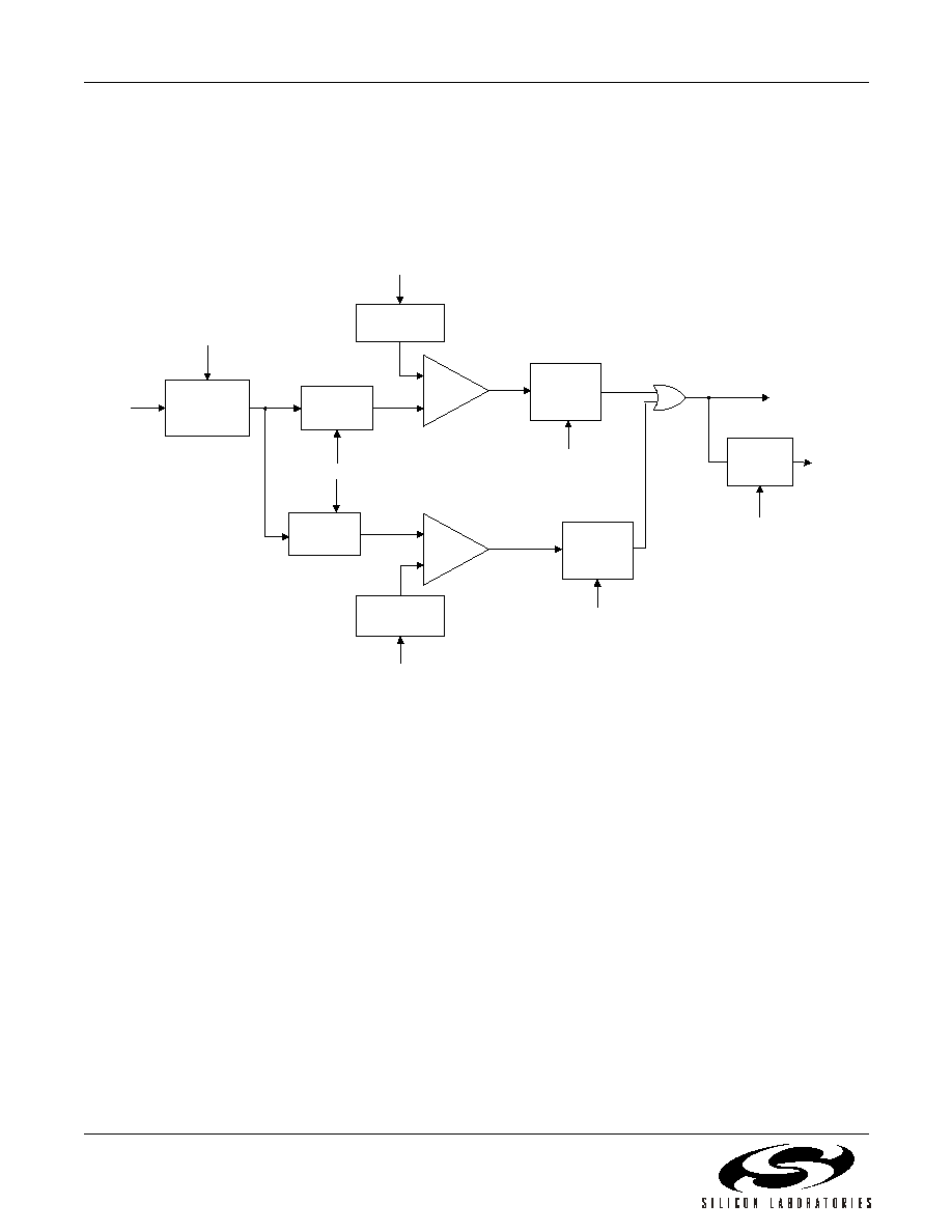
Si3232
42
Preliminary Rev. 0.96
4.11. Loop Closure Mask
The Dual ProSLIC implements a loop closure mask to
ensure mode change between Ringing and Active or
On-hook Transmission without causing an erroneous
loop-closure detection. The loop-closure mask register,
LCRMASK, should be set such that loop-closure
detections are ignored for (LCRMASK x 1.25 ms/LSB)
amount of time. The programmed time is set to mask
detection of transitional currents that occur when exiting
the ringing mode while driving a reactive load (i.e.,
5 REN). A typical setting is 80 ms (LCRMASK = 0x40).
Figure 20. Ring Trip Detect Processing Circuitry
Input
Signal
Processor
Digital
LPF
+
_
AC Ring Trip
Threshold
RTPER
LFS
ILOOP
RTACTH
Debounce
Filter_AC
Interrupt
Logic
RTRIPS
RTP
RTRIPE
+
_
DC Ring Trip
Threshold
RTDCTH
RTACDB
Digital
LPF
Debounce
Filter_DC
RTDCDB

Si3232
Preliminary Rev. 0.96
43
Table 24. Recommended Ring Trip Detection Values
1
Ringing
Frequency
DC Offset
Added?
RTPER
RTACTH
RTDCTH
RTACDB/
RTDCDB
16�32 Hz
Yes
800/f
RING
221 x RTPER
0.577(RTPER x V
OFF
)
See
Note 2
No
800/f
RING
1.59 x V
RING,PK
x RTPER
32767
33�60 Hz
Yes
2(800/f
RING
)
221 x RTPER
0.577(RTPER x V
OFF
)
No
2(800/f
RING
)
1.59 x V
RING,PK
x RTPER
32767
Notes:
1. All calculated values should be rounded to the nearest integer.
2. Refer to Ring Trip Debounce Interval for RTACDB and RTDCDB equations.
Table 25. Register and RAM Locations for Ring Trip Detection
Parameter
Register/RAM
Mnemonic
Register/
RAM Bits
Programmable
Range
Resolution
Ring Trip Interrupt Pending
IRQVEC2
RTRIPS
Yes/No
N/A
Ring Trip Interrupt Enable
IRQEN2
RTRIPE
Enabled/Disabled
N/A
AC Ring Trip Threshold
RTACTH
RTACTH[15:0]
See Table 24
DC Ring Trip Threshold
RTDCTH
RTDCTH[15:0]
See Table 24
Ring Trip Sample Period
RTPER
RTPER[15:0]
See Table 24
Linefeed Shadow (monitor only)
LINEFEED
LFS[2:0]
N/A
N/A
Ring Trip Detect Status (monitor only)
LCRRPT
RTP
N/A
N/A
AC Ring Trip Detect Debounce Interval
RTACDB
RTACDB[15:0]
0 to 40.96 s
1.25 ms
DC Ring Trip Detect Debounce Interval
RTDCDB
RTDCDB[15:0]
0 to 40.96 s
1.25 ms
Loop Current Sense (monitor only)
ILOOP
ILOOP[15:0]
0 to 101.09 mA
See Table 14

Si3232
44
Preliminary Rev. 0.96
4.12. Relay Driver Considerations
The Si3232 includes a general-purpose driver output for
each channel (GPOa, GPOb) to drive external test
relays. In most applications, the relay can be driven
directly from the Si3232 with no external relay drive
circuitry required. Figure 21 illustrates the internal relay
driver circuitry using a 3 V relay.
Figure 21. Si3232 Internal Relay Drive Circuitry
The internal driver logic and drive circuitry is powered
from the same 3.3 V supply as the chip's main supply
(VDD1�VDD4 pins). When operating external relays
from a V
CC
supply that is equal to the chip's V
DD
supply,
an internal diode network provides protection against
overvoltage conditions caused by flyback spikes when
the relay is opened. Only 3 V relays may be used in the
configuration shown in Figure 21, and either polarized
or non-polarized relays are acceptable provided both
V
CC
and V
DD
are powered by a 3.3 V supply. The input
impedance, R
IN
, of the relay driver pins is a constant
11
while sinking less than the maximum rated 85 mA
into the pin.
If the desired operating voltage of the relay, V
CC
, is
higher than the Si3232's V
DD
supply voltage, an
external drive circuit is required to eliminate leakage
from V
CC
to V
DD
through the internal protection diode.
In this configuration, a polarized relay is recommended
to provide optimal overvoltage protection with minimal
external components. Figure 22 illustrates the required
external drive circuit, and Table 26 provides
recommended values for R
DRV
for typical relay
characteristics and V
CC
supplies. The output
impedance, R
OUT
, of the relay driver pins is a constant
63
while sourcing less than the maximum rated
28 mA out of the pin.
Figure 22. Driving Relays with V
CC
> V
DD
The maximum allowable R
DRV
value can be calculated
using the following equation:
where
Q1,MIN
~ 30 for a 2N2222
Si3232
Relay
Driver
Logic
V
DD
GND
GPOa/b
V
CC
3 V/5 V Relay
(polarized or
non-polarized)
Table 26. Recommended R
DRV
Values
ProSLIC
V
DD
Relay
V
CC
Relay
R
COIL
Maximum
R
DRV
Recom-
mended
5% Value
3.3 V
�5%
3.3 V
�5%
64
Not
Required
--
3.3 V
�5%
5 V
�5%
178
2718
2.7 k
3.3 V
�5%
12 V
�10%
1028
6037
5.6 k
3.3 V
�5%
24 V
�10%
2880
8364
8.2 k
3.3 V
�5%
48 V
�10%
7680
11092
11 k
Si3232
V
DD
GPOa
GPOb
V
CC
Polarized
relay
R
DRV
I
DRV
Q1
MaxR
DRV
V
DD,MIN
0.6 V
�
(
) R
RELAY
(
)
Q1,MIN
(
)
V
CC,MAX
0.3 V
�
------------------------------------------------------------------------------------------------- R
SOURCE
�
=

Si3232
Preliminary Rev. 0.96
45
4.12.1. Polarity Reversal
The Si3232 supports polarity reversal for message-
waiting functionality as well as various signaling modes.
The ramp rate can be programmed for a smooth
transition or an abrupt transition to accommodate
different application requirements. A wink function is
also provided for special equipment that responds to a
smooth ramp to V
OC
= 0 V. Table 27 illustrates the
register bits required to program the polarity-reversal
modes.
An immediate reversal (hard reversal) of the line polarity
is achieved by setting the Linefeed register to the
opposite polarity. For example, a transition from
Forward Active mode to Reverse Active mode is
achieved by changing LF[2:0] from 001 to 101. Polarity
reversal can also be accommodated in the OHT and
ground-start modes. The POLREV bit is a read-only bit
that reflects whether the device is in polarity reversal
mode. A smooth polarity reversal is achieved by setting
the PREN bit to 1 and setting the RAMP bit to 0 or 1
depending on the desired ramp rate (see Table 27).
Polarity reversal is then accomplished by toggling the
linefeed register from forward to reverse modes as
desired.
A wink function is used to slowly ramp down the TIP-
RING voltage (V
OC
) to 1 followed by a return to the
original VOC value (set in the VOC RAM 0 location).
This scheme is used to light a message-waiting lamp in
certain handsets. To enable this function, no change to
the linefeed register is necessary. Instead, the user
must set the VOCZERO bit to 1 to cause the TIP-RING
voltage to collapse to 0 V at the rate programmed by the
RAMP bit. Setting the VOCZERO bit back to 0 causes
the TIP-RING voltage to return to its normal setting. A
software timer provided by the user can automate the
cadence of the wink function. Figure 23 illustrates the
wink function.
Table 27. Register and RAM Locations used for Polarity Reversal
Parameter
Programmable Range
Register/RAM Bits
Location
Linefeed See
Table 12
LF[2:0]
LINEFEED
Polarity Reversal Status
Read only
POLREV
POLREV
Wink Function
(Smooth transition to Voc = 0 V)
1 = Ramp to 0 V
0 = Return to previous V
OC
VOCZERO
POLREV
Smooth Polarity Reversal Enable
0 = Disabled
1 = Enabled
PREN
POLREV
Smooth Polarity Reversal Ramp
Rate
0 = 1 V/125 �s
1 = 2 V/125 �s
RAMP
POLREV
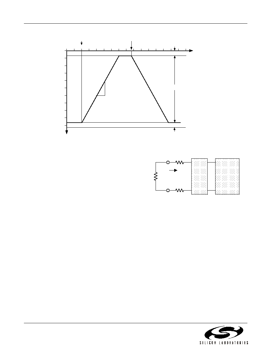
Si3232
46
Preliminary Rev. 0.96
Figure 23. Wink Function with Programmable Ramp Rate
4.13. Two-Wire Impedance Synthesis
Two-wire impedance synthesis is performed on-chip to
optimally match the output impedance of the Si3232 to
the impedance of the subscriber loop, thus minimizing
the receive path signal reflected back onto the transmit
path. The Si3232 provides on-chip selectable analog
two-wire impedances to meet return loss requirements.
The subscriber loop varies with any series impedance
due to protection devices placed between the Si3200
outputs and the TIP/RING pair according to the
following equation:
Where:
Z
T
is the termination impedance presented
to the TIP/RING pair
R
PROT
is the series resistance caused by
protection devices
R
A
is the analog portion of the selected
impedance
Therefore, the user must also consider the value of
R
PROT
when programming the on-chip analog
impedance.
The Si3232's analog impedance synthesis scheme is
sufficient for many short loop applications. If a unique
complex ac impedance is required, the Si3232's
impedance scheme must be augmented or replaced by
a DSP-based impedance generator. To turn off the
analog impedance coefficients (RS, ZP, and ZZ), set the
ZSDIS bit of the ZZ register to 0.
Figure 24. Two-Wire Impedance Simplified
Circuit
4.13.1. Transhybrid Balance Filter
The Si3232 is intended to be used with DSP-based
codecs that provide the transhybrid balance function.
No transhybrid capability exists in the Si3232.
4.13.2. Pulse Metering Generation
The Si3232 offers an internal tone generator suitable for
generating tones above the audio frequency band. This
oscillator is provided for the generation of billing tones
which are typically 12 kHz or 16 kHz. The equations for
calculating the pulse metering coefficients are as
follows:
Coeff = cos (2
f/64000 Hz)
PMFREQ = coeff
�
(2
14
� 1)
V
TIP/RING
(V)
0
-10
-20
-30
-40
-50
Time (ms)
50
40
30
20
10
60
70
80
0
2V/125 �s slope
set by RAMP bit
Set VOCZERO bit to 1
Set VOCZERO bit to 0
V
cm
V
ov
V
oc
V
TIP
V
BAT
V
RING
Z
T
2R
PROT
R
A
+
=
Si3232
Z
T
Z
L
R
PROT
R
PROT
Si32
00
TIP
RING

Si3232
Preliminary Rev. 0.96
47
where Full Scale V
PK
= 0.5 V.
The pulse metering oscillator has a volume envelope
(linear ramp) on the on/off transitions of the oscillator.
The ramp is controlled by the value entered into the
PMRAMP RAM address, and the sinusoidal generator
output is multiplied by this volume before being sent to
the pulse metering DAC. The volume value is
incremented by the value in PMRAMP at an 8 kHz rate.
The volume ramps from 0 to 7FFF in increments of
PMRAMP, thus allowing the value of PMRAMP to set
the slope of the ramp. The clip detector stops the ramp
once the signal seen at the transmit path exceeds the
amplitude threshold set by PMAMPTH, thus providing
an automatic gain control (AGC) function to prevent the
audio signal from clipping. When the pulse metering
signal is turned off, the volume ramps down to 0 by
decrementing according to the value of PMRAMP.
Figure 24 illustrates the functional blocks involved in
pulse-metering generation, and Table 28 presents the
register and RAM locations required that must be set to
generate pulse-metering signals.
PMAMPL
1
4
--- 1 coeff
�
1 coeff
+
------------------------
2
15
1
�
(
)
�
Desired V
PK
Full Scale V
PK
------------------------------------------
�
=
Table 28. Register and RAM Locations Used for Pulse Metering Generation
Parameter
Register/RAM
Mnemonic
Register/RAM
Bits
Description / Range
(LSB Size)
Pulse-Metering Frequency
Coefficient
PMFREQ
PMFREQ[15:3]
Sets oscillator frequency
Pulse-Metering Amplitude
Coefficient
PMAMPL
PMAMPL[15:0]
Sets oscillator amplitude
Pulse-Metering Attack/Decay
Ramp Rate
PMRAMP
PMRAMP[15:0]
0 to PMAMPL
(full amplitude)
Pulse-Metering Active Timer
PMTALO/PMTAHI
PULSETA[15:0]
0 to 8.19 s (125 �s)
Pulse-Metering Inactive Timer
PMTILO/PMTIHI
PULSETI[15:0]
0 to 8.19 s (125 �s)
Pulse-Metering,
Control Interrupt
IRQVEC1,
IRQEN1
PULSTAE,
PULSTIE,
PULSTAS,
PULSTIS
Interrupt status and control
registers
Pulse-Metering AGC
Amplitude Threshold
PMAMPTH
PMAMPTH[15:0]
0 to 500 mV
PM Waveform Present
PMCON
ENSYNC
Indicates Signal Present
PM Active Timer Enable
PMCON
TAEN1
Enable/disable
PM Inactive Timer Enable
PMCON
TIEN1
Enable/disable
Pulse-Metering Enable
PMCON
PULSE1
Enable/disable
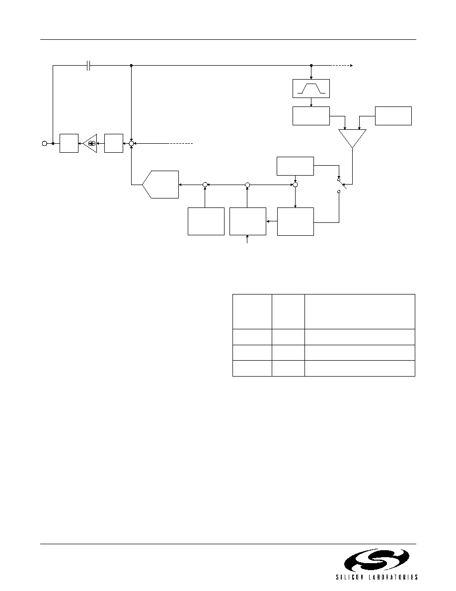
Si3232
48
Preliminary Rev. 0.96
Figure 25. Pulse Metering Generation Block Diagram
4.14. Audio Path Processing
The Si3232 is designed to connect directly to integrated
access device (IAD) chipsets, such as the Broadcom
BCM3341, as well as other standard codecs that use a
differential audio interface. Figure 3 on page 15
illustrates the simplified block diagram for the Si3232.
4.14.1. Transmit Path
In the transmit path, the analog signal fed by the
external ac-coupling capacitors, C1 and C2, is amplified
by the analog transmit amplifier, ATX, prior to the
differential analog output to the A/D converter in the
external codec. The ATX stage can be used to add 3 dB
of attenuation by programming the ATX bit of the
AUDGAIN register. A mute function is also available by
setting the ATXMUTE bit of the AUDGAIN register to 1.
The main role of the ATX stage is to attenuate incoming
signals to best match the input scale of the external A/D
converter to maximize signal-to-noise ratio.
The resulting gain levels using the ATX stage are
summarized in Table 29. All settings assume a 0 dBm0
TIP-RING audio input signal with the audio TX level
measured differentially at VTXPa-VTXNa (for channel
a) or VTXPb-VTXNb (for channel b).
4.14.2. Receive Path
In the receive path, the incoming audio signal from the
D/A converter in the external codec is passed through
an ARX stage where the user can attenuate audio
signals in the analog domain prior to transmission to
TIP/RING. Settings of 0, �3, and �6 dB are available by
programming the ARX[1:0] bits of the AUDGAIN
register to the appropriate settings. A mute function is
also available by setting the ARXMUTE bit of the
AUDGAIN register to 1. When not muted, the resulting
analog signal is applied at the input of the
transconductance amplifier, Gm, which drives the off-
chip current buffer, I
BUF
.
Pulse
Metering
DAC
Pulse
Metering
Oscillator
Volume
PMRAMP
Peak Detector
PMAMPTH
Z
A
I
BUF
+
+
�
+
8 kHz
7FFF
or 0
Clip
Logic
� +
12/16 kHz
Bandpass
To VTX outputs
From VRX inputs
+
Table 29. ATX Attenuation Stage Settings
ATXMUT
E
Setting
ATX
Setting
Typical TX Path Gain
1
X
Mute (no output)
0
0
�1.584 dB (G = 10/12)
0
1
�4.682 dB (G = 7/12)

Si3232
Preliminary Rev. 0.96
49
The resulting gain levels using the ARX stage are
summarized in Table 30. All settings assume an
external codec with 475
per leg of source impedance
driving the RX inputs differentially at VRXPa-VRXNa
(for channel a) or VRXPb-VRXNb (for channel b) to
achieve a 0 dBm0 TIP-RING audio output signal.
4.15. System Clock Generation
The Si3232 generates the necessary internal clock
frequencies from the PCLK input. PCLK must be
synchronous to the 8 kHz FSYNC clock and run at one
of the following rates: 256 kHz, 512 kHz, 786 kHz,
1.024 MHz, 1.536 MHz, 1.544 MHz, 2.048 MHz,
4.096 MHz, or 8.192 MHz. The ratio of the PCLK rate to
the FSYNC rate is determined by a counter clocked by
PCLK. The 3-bit ratio information is automatically
transferred into an internal register, PLL_MULT,
following a device reset. PLL_MULT is used to control
the internal PLL, which multiplies PCLK as needed to
generate the rate required to run the internal filters and
other circuitry.
The PLL clock synthesizer settles quickly after powerup
or update of the PLL-MULT register. The PLL lock
process begins immediately after the RESET pin is
pulled high and will take approximately 5 ms to achieve
lock after RESET is released with stable PCLK and
FSYNC. However, the settling time depends on the
PCLK frequency and can be predicted based on the
following equation:
t
SETTLE
= 64 / f
PCLK
Note: Therefore, the RESET pin must be held low during
powerup and should only be released when both PCLK
and FSYNC signals are known to be stable.
4.15.1. Interrupt Logic
The Si3232 is capable of generating interrupts for the
following events:
Loop current/ring ground detected.
Ground key detected.
Ring trip detected.
Power alarm.
Ringing active timer expired.
Ringing inactive timer expired.
Pulse metering active timer expired.
Pulse metering inactive timer expired.
RAM address access complete.
The interface to the interrupt logic consists of six
registers. Three interrupt status registers (IRQ0�IRQ3)
contain one bit for each of the above interrupt functions.
These bits are set when an interrupt is pending for the
associated resource. Three interrupt mask registers
(IRQEN1�IRQEN3) also contain one bit for each
interrupt function. In the case of the interrupt mask
registers, the bits are active high. Refer to the
appropriate functional description text for operational
details of the interrupt functions.
Figure 26. PLL Frequency Synthesizer
Table 30. ARX Attenuation Stage Settings
ARXMUTE
Setting
ARX[1:0]
Setting
Typical TX Path Gain
1
xx
Mute (no T-R output)
0
00
0 dB (G = 1)
0
01
�3.52 dB (G = 2/3)
0
10
�6.02 dB (G = 1/2)
0
11
Reserved. Do not use.
PFD
DIV M
PLL_MULT
VCO
�2
�2
RESET
28.672 MHz
PCLK

Si3232
50
Preliminary Rev. 0.96
When a resource reaches an interrupt condition, it
signals an interrupt to the interrupt control block. The
interrupt control block then sets the associated bit in the
interrupt status register if the mask bit for that interrupt
is set. The INT pin is a NOR of the bits of the interrupt
status registers. Therefore, if a bit in the interrupt status
registers is asserted, IRQ asserts low. Upon receiving
the interrupt, the interrupt handler should read interrupt
status registers to determine which resource is
requesting service. All interrupt bits in the interrupt
status registers, IRQ0�IRQ3, are cleared following a
register read operation. While the interrupt status
registers are non-zero, the INT pin remains asserted.
4.16. SPI Control Interface
The Si3232 has a 4-wire serial peripheral interface
(SPI) control bus modeled after commonly-available
micro-controller and serial peripheral devices. The
interface consists of a clock (SCLK), chip select (CSB),
serial data input (SDI), and serial data output (SDO). In
addition, the Si3232 includes a serial data through
output (SDI_THRU) to support daisy chain operation of
up to eight devices (up to sixteen channels). The device
can operate with both 8-bit and 16-bit SPI controllers.
Each SPI operation consists of a control byte, an
address byte (of which only the seven LSBs are used
internally), and either one or two data bytes depending
on the width of the controller and whether the access is
to a direct or indirect register. Bytes are always
transmitted MSB first.
There are a number of variations of usage on this four-
wire interface as follows:
Continuous clocking
. During continuous clocking,
the data transfers are controlled by the assertion of
the CSB pin. CSB must be asserted before the
falling edge of SCLK on which the first bit of data is
expected during a read cycle and must remain low
for the duration of the 8-bit transfer (command/
address or data), going high after the last rising of
SCLK after the transfer.
Clock only during transfer
. In this mode, the clock
cycles only during the actual byte transfers. Each
byte transfer will consist of eight clock cycles in a
return to 1 format.
SDI/SDO wired operation
. Independent of the
clocking options described, SDI and SDO can be
treated as two separate lines or wired together if the
master is capable of tri-stating its output during the
data byte transfer of a read operation.
Soft reset
. The SPI state machine resets whenever
CSB is asserted during an operation on an SCLK
cycle that is not a multiple of eight. This provides a
mechanism for the controller to force the state
machine to a known state in the case where the
controller and the device appear to be out of
synchronization.
The control byte has the following structure and is
presented on the SDI pin MSB first. The bits are defined
in Table 31.
7
6
5
4
3
2
1
0
BRDCST
R/W
REG/RAM Reserved
CID[0]
CID[1]
CID[2]
CID[3]

Si3232
Preliminary Rev. 0.96
51
Refer to "2. Typical Application Schematic" on page 17.
The pulldown resistor on the SDO pin is required to
allow this node to discharge after a logic high state to a
tri-state condition. The discharge occurs while SDO is
tri-stated during an 8 kHz transmission frame. The value
of the pulldown resistor depends on the capacitance
seen on the SDO pin. In the case of using a single
Si3232, the value of the pulldown resistor is 39 k
. This
assumes a 5 pF SDO pin capacitance and about a
15 pF load on the SDO pin. For applications using
multiple Si3232 devices or different capacitive loads on
the SDO pin, a different pulldown resistance needs to
be calculated.
The following design procedure is an example for
calculating the pulldown resistor on the SDO pin in a
system using eight Si3232 devices. A pullup resistor is
not allowed on the SDO pin.
1. The SDO node must discharge and remain discharged for
244 ns. The discharge occurs during the Hi-Z state;
therefore, the time to discharge is equal to the time in Hi-Z
time minus the 244 ns.
2. Allow five time constants for discharge where the
time constant, t = RC
3. SDO will be in Hi-Z while SDI is sending control and
address which are each 8 bits. Using the maximum
SCLK frequency of 16.13 MHz, the SDO will be in
Hi-Z for 16 / 16.13 MHz = 992 ns.
4. We want to discharge and remain discharged for
244 ns. Therefore, the discharge time is:
992 ns � 244 ns = 748 ns
5. To allow for some margin, let's discharge in 85% of
this time. 748nS x 85% = 635.8 ns
6. Determine capacitive load on the SDO pin:
a.Allow 5 pF for each Si3220 SDO pin that
connected together.
b.Allow ~2 pF/inch (~0.8 pF/cm) for PCB trace.
c.Include the load capacitance of the host IC input.
7. For a system with eight Si3220 devices, the
capacitance seen on the SDO pin would be:
a.8 x 5 pF for each Si3220 = 40 pF
b.Assume 5 inch of PCB trace: 5inch x 2 pF/
inch = 10 pF
c.Host IC input of 5 pF
d.Total capacitance is 55 pF
8. Using the equation t = RC, allowing five time
constants to decay, and solving for R
a.R = t / 5C = 635.8 ns / (5 x 55 pF)
b.R = 2.3 k
So, R must be less than 2.3 k
to allow the node to
discharge.
Table 31. SPI Control Interface
7
BRDCST Indicates a broadcast operation that is intended for all devices in the daisy chain. This is
only valid for write operations since it would cause contention on the SDO pin during a
read.
6
R/W
Read/Write Bit.
0 = Write operation.
1 = Read operation.
5
REG/RAM Register/RAM Access.
0 = RAM access.
1 = Register access.
4
Reserved
3:0
CID[3:0]
This field indicates the channel that is targeted by the operation. The 4-bit channel value is
provided LSB first. The devices reside on the daisy chain such that device 0 is nearest to
the controller, and device 15 is furthest down the SDI/SDU_THRU chain. (See Figure 26.)
As the CID information propagates down the daisy chain, each channel decrements the
CID by 1. The SDI nodes between devices will reflect a decrement of 2 per device since
each device contains two channels. The device receiving a value of 0 in the CID field will
respond to the SPI transaction. (See Figure 27.) If a broadcast to all devices connected to
the chain is requested, the CID will not decrement. In this case, the same 8-bit or 16-bit
data is presented to all channels regardless of the CID values.

Si3232
52
Preliminary Rev. 0.96
4.17. Si3232 RAM and Register Space
The Si3232 is a highly-programmable telephone
linecard solution that uses internal registers and RAM to
program operational parameters and modes. The
Register Summary and RAM Summary are compressed
listings for single-entry quick reference. The Register
Descriptions and RAM Descriptions give detailed
information of each register or RAM location's bits.
All RAM locations are cleared upon a hardware reset.
All RAM locations that are listed as "INIT" must be
initialized to a meaningful value for proper functionality.
Bit 4 of the MSTRSTAT register indicates the clearing
process is finished. This bit should be checked before
initializing the RAM space.
Accessing register and RAM space is performed
through the SPI. Register space is accessed by using
the standard three-byte access as described in the next
section. Bit 5 of the control byte specifies register
access when set to a 1. All register space is comprised
of 8-bit data.
4.17.1. RAM Access by Pipeline
Ram space can be accessed by two different methods.
One method is a pipeline method that employs a 4-byte
access plus a RAM status check. The control byte for
the pipeline method has bit 6 cleared to 0 to indicate a
RAM access. The control byte is followed by the RAM
address byte, then the two data bytes.
Reading RAM in the pipeline method requires "priming"
the data. First, check for register RAMSTAT, bit 0, to
indicate the previous access is complete and RAM is
ready (0). Then, perform the 4-byte RAM access. The
first read will yield unusable data. The data read on the
subsequent read access is the data for the previous
address read. A final address read yields the last
previously-requested data. The RAM-ready information
(RAMSTAT) must be read before every RAM access.
To write a RAM location, check for register RAMSTAT,
bit 0, to indicate the previous access is complete and
RAM is ready (0). Then, write the RAM address and
data in the 4-byte method. A write to RAM location
requires "priming" the data with subsequent accesses.
4.17.2. RAM Access by Register
An alternative method to access RAM space utilizes
three registers in sequence and monitors RAMSTAT
register, bit 0. These three registers are RAMADDR,
RAMDATLO, and RAMDATHI.
To read a RAM location in the Si3232, check for register
RAMSTAT (bit 0) to indicate the previous access is
complete and RAM is ready (0). Then, write the RAM
address to RAMADDR. Wait until RAMSTAT (bit 0) is a
1; then, the 16 bits of data can be read from the
RAMDATLO and RAMDATHI registers.
To write a RAM location in the Si3232, check for register
RAMSTAT (bit 0) to indicate the previous access is
completed and RAM is ready (0); then, write the 16 bits
of RAM data to the RAMDATLO, RAMDATHI. Finally,
write the RAM address to the RAMADDR register.
4.17.3. Chip Select
For register or RAM space access, there are three ways
to use chip select: byte length, 16-bit length, and access
duration length. The byte length method releases chip
select after every 8 bits of communication with the
Si3232. The time between chip select assertions must
be at least 220 ns.
The 16-bit length chip select method is similar to the
byte length method except that 16-bits are
communicated with the Si3232. This means that Si3232
communication consists of a control byte, address byte
for one 16-bit access, and two data bytes for a second
16-bit access.
In a single data byte communication (control byte,
address byte, data byte), the data byte should be
loaded into either the high byte or both bytes of the
second 16-bit access for a write. The 8-bit data exists in
the high and low byte of a 16-bit access for a read. The
time between chip select assertion must be at least
220 ns.
Access duration length allows chip select to be pulled
low for the length of a number of Si3232 accesses.
There are two very specific rules for this type of
communication. One rule is that the SCLK must be of a
frequency that is less than 1/2x220 ns (<2.25 MHz).
The second rule is that access must be done in a 16-bit
modulus. This 16-bit modulus follows the same rules as
described above for 16-bit length access where 8-bit
data is concerned.
4.17.4. Protected Register Bits
The Si3232 has protected register bits that are meant to
retain the integrity of the Si3232 circuit in the event of
unintentional software register access. To access the
user-protected bits, write the following sequence of data
bytes to register address 87 (0x57):
0x02
0x10
0x12
0x00
Following the modification of any protected bit, the
same sequence should be immediately written to place
these bits into their protected state.
Protected bits exist in registers SBIAS and THERM.

Si3232
Preliminary Rev. 0.96
53
Figure 27. SPI Daisy Chain Control Architecture
CPU
Channel 0
Channel 1
SDO
SDI
SDI
SDITHRU
Si3232 #8
Si3232 #2
Si3232 #1
CS
CS
SDO
Channel 2
Channel 3
SDI
SDITHRU
CS
SDO
Channel 14
Channel 15
SDI
SDITHRU
SDO
CS
SDI0
SDI1
SDI2
SDI3
SDI4
SDI15
SDI14
SCLK
SPI Clock
SCLK
SCLK

Si3232
54
Preliminary Rev. 0.96
In Figure 28, the CID field is 0. As this field is decremented (LSB to MSB order), the value decrements for each SDI
down the line. The BRDCST, R/W, and REG/RAM bits remain unchanged as the control word passes through the
entire chain. The odd SDIs are internal to the device and represent the SDI to SDI_THRU connection between
channels of the same device. A unique CID is presented to each channel, and the channel receiving a CID value of
0 is the target of the operation (channel 0 in this case). The last line of Figure 28 illustrates that in broadcast mode,
all bits are passed through the chain without permutation.
Figure 28. Sample SPI Control Word to Address Channel 0
Figure 29. Register Write Operation via an 8-Bit SPI Port
SPI Control Word
BRDCST
R/W
REG/RAM
Reserved
CID[0]
CID[1]
CID[2]
CID[3]
0
A
B
C
0
0
0
0
0
A
B
C
1
1
1
1
0
A
B
C
0
1
1
1
0
A
B
C
1
0
1
1
0
A
B
C
0
1
0
0
0
A
B
C
1
0
0
0
1
A
B
C
D
E
F
G
SDI0
SDI1 (Internal)
SDI2
SDI3 (Internal)
SDI 0-15
SDI15
SDI0-15
CONTROL
ADDRESS
DATA [7:0]
SCLK
SDI
SDO
Hi-Z
CS

Si3232
Preliminary Rev. 0.96
55
Figures 29 and 30 illustrate WRITE and READ operations to registers via an 8-bit SPI controller. These operations
are each performed as a 3-byte transfer. CS is asserted between each byte. It is necessary for CS to be asserted
before the first falling edge of SCLK after the DATA byte to indicate to the state machine that only one byte should
be transferred. The state of SDI is a "don't care" during the DATA byte of a read operation.
Figures 31 and 32 illustrate WRITE and READ operation to registers via a 16-bit SPI controller. These operations
require a 4-byte transfer arranged as two 16-bit words. The absence of CS going high after the eighth bit of data
indicates to the SPI state machine that eight more SCLK pulses will follow to complete the operation. In the case of
a WRITE operation, the last eight bits are ignored. In the case of a read operation, the 8-bit data value is repeated
so that the data can be captured during the last half of a data transfer if so desired by the controller.
During register accesses, the CONTROL, ADDRESS, and DATA are captured in the SPI module. At the completion
of the ADDRESS byte of a READ access, the contents of the addressed register are moved into the data register in
the SPI. At the completion of the DATA byte of a WRITE access, the data is transferred from the SPI to the
addressed register location.
Figure 30. Register Read Operation via an 8-Bit SPI Port
Figure 31. Register Write Operation via a 16-Bit SPI Port
Figure 32. Register Read Operation via a 16-Bit SPI Port
CONTROL
ADDRESS
X X X X X X X X
SCLK
SDI
SDO
Data [7:0]
CS
X X X X X X X X
SCLK
SDI
SDO
CONTROL
ADDRESS
Data [7:0]
Hi - Z
CS
X X X X X X X X
SCLK
SDI
SDO
Data [7:0]
CONTROL
ADDRESS
X X X X X X X X
Data [7:0]
Same byte repeated twice.
CS
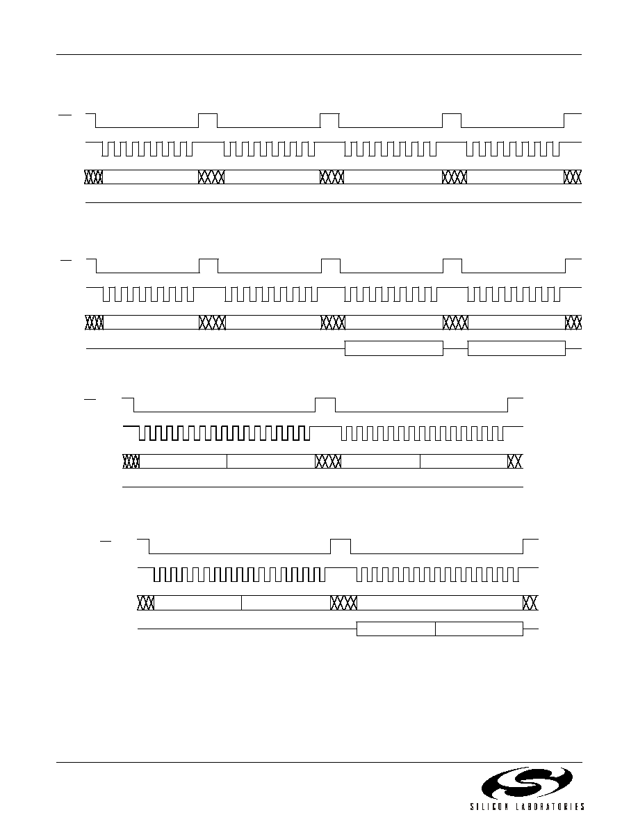
Si3232
56
Preliminary Rev. 0.96
Figures 33�36 illustrate the various cycles for accessing RAM address locations. RAM addresses are 16-bit
entities; therefore the accesses always require four bytes.
Figure 33. RAM Write Operation via an 8-Bit SPI Port
Figure 34. RAM Read Operation via an 8-Bit SPI Port
Figure 35. RAM Write Operation via a 16-Bit SPI Port
Figure 36. RAM Read Operation via a 16-Bit SPI Port
SCLK
SDI
SDO
CONTROL
ADDRESS
DATA [15:8]
DATA [7:0]
Hi-Z
CS
SCLK
SDI
SDO
x x x x x x x x
x x x x x x x x
DATA [15:8]
DATA [7:0]
CS
SCLK
SDI
SDO
CONTROL
ADDRESS
Data [15:8]
Hi - Z
Data [7:0]
CS
SCLK
SDI
SDO
CONTROL
ADDRESS
Data [15:8]
Data [7:0]
x x x x x x x x x x x x x x x x
CS

Si3232
Preliminary Rev. 0.96
57
During RAM address accesses, CONTROL,
ADDRESS, and DATA are captured in the SPI module.
At the completion of the ADDRESS byte of a READ
access, the contents of the channel-based data buffer
are moved into the data register in the SPI for shifting
out during the DATA portion of the SPI transfer. This is
the data loaded into the data buffer in response to the
previous RAM address read request. Therefore, there is
a one-deep pipeline nature to RAM address READ
operations. At the completion of the DATA portion of the
READ cycle, the ADDRESS is transferred to the
channel-based address buffer, and a RAM access
request is logged for that channel. The RAMSTAT bit in
each channel can be polled to monitor the status of
RAM address accesses that are serviced twice per
sample period at dedicated windows in the DSP
algorithm.
There is also a RAM access interrupt in each channel
which, when enabled, indicates that the pending RAM
access request has been serviced. For a RAM WRITE
access, the ADDRESS and DATA is transferred from
the SPI registers to the address and data buffers in the
appropriate channel. The RAM WRITE request is then
logged. As for READ operations, the status of the
pending request can be monitored by either polling the
RAMSTAT bit for the channel or enabling the RAM
access interrupt for the channel. By keeping the
address and data buffers as well as the RAMSTAT
register on a per-channel basis, RAM address accesses
can be scheduled for both channels without interface.
4.18. System Testing
The Si3232 includes a complete suite of test tools that
provide the user with the ability to test the functionality
of the line card as well as detect fault conditions present
on the TIP/RING pair. Using the included loopback test
mode along with the signal generation and
measurement tools, the user can typically eliminate the
need for per-line test relays as well as centralized test
equipment.
4.18.1. Loopback Test Mode
The codec loopback encompasses almost entirely the
electronics of both the transmit and receive paths. The
analog signal at the output of the system receive path
DAC is fed back to the input of the transmit path by way
of a feedback path. (See Figure 37.) The codec
loopback mode is enabled by setting the DLM bit in the
LBCON register. The impedance synthesis is disabled
in this mode.
4.18.2. Line Test and Diagnostics
The Si3232 provides a variety of diagnostics tools that
facilitate remote fault detection and parametric
diagnostics on the TIP/RING pair as well as line card
functionality verification. The Si3232 can generate dc
line currents and voltages as well as measure all
resulting line voltage and current levels on TIP, RING, or
across the TIP/RING pair. When used in conjunction
with an external codec that can generate discrete audio
tones and discriminate certain audio frequency bands,
the Si3232 can provide a vehicle to allow remote
diagnostics on the subscriber loop and the line card. All
parameters measured by the Si3232 are stored in
registers for further processing by the codec and DSP,
and all dc generation tools are register-programmable
to allow a software-configurable remote diagnostic
system.
The Si3232's signal generation and measurement tools
are summarized in Table 32. The accompanying text
describes the methodology that can be used to develop
a fully-programmable test suite to facilitate remote
diagnostics.
Figure 37. Digital Loopback Mode
TIP/
RING
+
ATX
I
BUF
Z
A
Codec
Loopback
To off-chip
ADC
Mute
+
Mute
G
m
ARX
From
off-chip
ADC

Si3232
58
Preliminary Rev. 0.96
4.18.3. Signal Generation Tools
TIP/RING dc signal generation.
The Si3232
linefeed D/A converter can program a constant
current linefeed from 18�45 mA in 0.87 mA steps
with a �10% total accuracy. In addition, the open-
circuit TIP/RING voltage can be programmed from 0
to 63 V in 1 V steps. The linefeed circuitry also has
the ability to generate a controlled polarity reversal.
Diagnostics mode ringing generation. The Si3232
can generate an internal low-level ringing signal to
test for the presence of REN without causing the
terminal equipment to ring audibly. This ringing
signal can be either balance or unbalanced
depending on the state of the RINGUNB bit of the
RINGCON register and the amplitude of the battery
supplies present.
4.18.4. Measurement Tools
8-Bit monitor A/D converter.
This 8-bit A/D
converter monitors all dc and low-frequency voltage
and current data from TIP to ground and RING to
ground. Two additional values, TIP-RING and
TIP+RING, are calculated and stored in on-chip
registers for analyzing metallic and longitudinal
effects. The A/D operates at an 800 Hz update rate
to allow measurement bandwidth from dc to 400 Hz.
A dual-range capability allows high-voltage/high-
current measurement in the high range but can also
measure lower voltages and currents with a tighter
resolution.
AC
rms
, AC
PK
and dc filter blocks.
Several post-
processing filter blocks are provided to allow the
measured parameters to be processed according to
the desired result.
SLIC diagnostics filter
Several post-processing filter blocks are provided for
monitoring PEAK, dc, and ac characteristics of the
Monitor A/D converter outputs as well as values
derived from these outputs. Setting the SDIAG bit in
the DIAG register enables the filters. There are
separate filters for each channel, and their control is
independent.
The following parameters can be selected as inputs
to the diagnostic block by setting the SDIAG_IN bits
in the DIAG register to values 0�5 corresponding to
the order below:
V
TIP
= voltage on the TIP lead
V
RI NG
= voltage on the RING lead
V
LOOP
=
V
TIP
�V
RING
=
metallic (loop) voltage
V
LONG
=
(V
TIP
+V
RING
)/2
=
longitudinal voltage
I
LOOP
=
I
TIP
�I
RING
=
metallic (loop) current
I
LONG
=
(I
TIP
+I
RING
)/2
=
longitudinal current
The SLIC diagnostic capability consists of a peak detect
block and two filter blocks, one for dc and one for ac.
The topology is illustrated in Figure 38.
Table 32. Summary of Signal Generation and Measurement Tools
Function
Range
Accuracy/
Resolution
Comments
Signal Generation Tools
DC Current Generation
18 to 45 mA
0.875 mA
DC Voltage Generation
0 to 63.3 V
1.005 V
Ringing Signal Generation
4 to 15 V
16 to 100 Hz
�5%
�1%
Measurement Tools
8-Bit DC/Low Frequency
Monitor A/D Converter
High Range:
0 to 160.173 V
0 to 101.09 mA
628 mV
396.4 �A
800 Hz update rate
AC
rms
, AC
PK
, and dc post-
processing blocks
Low Range: 0 to 64.07V
0 to 50.54 mA
251 mV
198.2 �A
AC Low-pass Filter
3 to 400 Hz

Si3232
Preliminary Rev. 0.96
59
Figure 38. SLIC Diagnostic Filter Structure
The peak detect filter block will report the magnitude of
the largest positive or negative value without sign. The
dc filter block consists of a single pole IIR low-pass filter
with a coefficient held in the DIAGDCCO indirect
register. The filter output can be read from the
DIAG_DC indirect register. The ac filter block consists of
a full-wave rectifier followed by a single-pole IIR low-
pass filter with a coefficient held in the DIAGACCO
indirect register. The peak value can be read from the
DIAGPK indirect register. The peak value is
automatically cleared, and the filters are flushed on the
0-1 transition of the SDIAG bit as well as any time the
input source is changed. The user can always write 0 to
the DIAGPK register to get peak information for a
specific time interval.
4.18.5. Diagnostics Capabilities
Foreign voltages test.
The Si3232 can detect the
presence of foreign voltages according to GR-909
requirements of ac voltages > 10 V and dc voltages
> 6 V from T-G or R-G. This test should only be
performed once it has been determined that a
hazardous voltage is not present on the line.
Resistive faults test.
Resistive fault conditions can
be measured from T-G, R-G, or T-R for dc resistance
per GR-909 specifications. If the dc resistance is
< 150 k
, it is considered a resistive fault. This test
can be performed by programming the Si3232 to
generate a constant open-circuit voltage and
measuring the resulting current. The resistance can
then be calculated in the system DSP.
Receiver off-hook test.
This test can use a similar
procedure as outlined in the Resistive Faults test
above but is measured only across T-R. In addition,
two measurements must be performed at different
open-circuit voltages in order to verify the resistive
linearity. If the calculated resistance has more than
15% nonlinearity between the two calculated points
and the voltage/current origin, it is determined to be
a resistive fault.
Ringers (REN) test.
This test verifies the presence
of REN at the end of the TIP/RING pair per GR-909
specifications. It can be implemented by generating
a 20 Hz ringing signal between 7 V
rms
and 17 V
rms
and measuring the 20 Hz ac current using the 8-bit
monitor ADC. The resistance (REN) can then be
calculated using the system DSP. The acceptable
REN range is > 0.175 REN (<40 k
) or < 5 REN
(> 1400
). A returned value of <1400 is
determined to be a resistive fault from T-R, and a
returned value > 40 k
is determined to be a loop
with no handset attached.
AC line impedance measurement.
This test can
determine the loop length across T-R. It can be
implemented by sending out multiple discrete tones
from the system DSP/codec, one at a time, and
measuring the returned amplitude, with the system
hybrid balance filter disabled. By calculating the
voltage difference between the initial amplitude and
the received amplitude and dividing the result by the
audio current, the line impedance can then be
calculated in the system processor.
Line capacitance measurement.
This test can be
implemented in the same manner as the ac line
impedance measurement
test above, but the
frequency band of interest is between 1 kHz and
3.4 kHz. Knowing the synthesized 2-wire impedance
of the Si3232, the roll-off effect can be used to
calculate the ac line capacitance. An external codec
is required for this test.
PEAK
DETECT
LPF
LPF
FULL WAVE
RECTIFIER
DIAGDCCO
DIAGACCO
SDIAG_PK
SDIAG_DC
SDIAG_AC
VTIP
VRING
VLOOP
VLONG
ILOOP
ILONG

Si3232
60
Preliminary Rev. 0.96
Ringing voltage verification.
This test verifies that
the desired ringing signal has been correctly applied
to the TIP/RING pair and can be measured in the 8-
bit monitor ADC, which senses low-frequency
signals directly across T-R.
Power induction measurement.
This test can
detect the presence of a power supply coupled onto
the TIP/RING pair. It can be implemented by
measuring the energy content at 50/60 Hz (normal
induction) or at 100/120 Hz (rectified power
induction). This is achieved by measuring the line
voltage using a low-pass filter in the system DSP on
the 8-bit monitor ADC while making certain there is
no ringing signal present on the line.

Si3232
Preliminary Rev. 0.96
61
5. 8-Bit Control Register Summary
1,2
Any register not listed here is reserved and must not be written. Shaded registers are read only. All registers are
assigned a default value during initialization and following a system reset. Only registers 0, 2, 3, and 14 are
available until a PLL lock is established or during a clock failure.
(Ordered alphabetically by mnemonic.)
Reg
Addr
3
Mnemonic
Description
Bit 7
Bit 6
Bit 5
Bit 4
Bit 3
Bit 2
Bit 1
Bit 0
Type
R/W
Def.
Hex
Audio
21
AUDGAIN
Audio Gain Control
CMTXSEL
ATXMUTE
ATX
ARXMUTE
ARX[1:0]
Init
R/W
0x00
Calibration
11
CALR1
Calibration Register 1
CAL
CALOFFR
CALOFFT
CALOFFRN
CALOFFTN
CALDIFG
CALCMG
Init
R/W
0x3F
12
CALR2
Calibration Register 2
CALLKGR
CALLKGT
CALMADC
CALDACO
CALADCO
CALCMBAL
Init
R/W
0x3F
Diagnostic Tools
13
DIAG
Diagnostics Tool Enable
IQ2HR
IQ1HR
TSTRING
TXFILT
SDIAG
SDIAGIN[2:0]
Diag
R/W
Chip ID
0
ID
Chip ID
PARTNUM[2:0]
4
REV[3:0]
4
Init
R
0x--
Loop Current Limit
10
ILIM
Loop Current Limit
ILIM[4:0]
Init
R/W
0x05
Interrupts
14
IRQ0
Interrupt Status 0
CLKIRQ
4,6
IRQ3B
4,6
IRQ2B
4,6
IRQ1B
4,6
IRQ3A
4,6
IRQ2A
4,6
IRQ1A
4,6
Oper
R
0x00
15
IRQ1
Interrupt Status 1
PULSTAS
PULSTIS
RINGTAS
RINGTIS
Oper
R/W
0x00
16
IRQ2
Interrupt Status 2
RAMIRS
DTMFS
VOCTRKS
LONGS
LOOPS
RTRIPS
Oper
R/W
0x00
17
IRQ3
Interrupt Status 3
CMBALS
PQ6S
PQ5S
PQ4S
PQ3S
PQ2S
PQ1S
Oper
R/W
0x00
18
IRQEN1
Interrupt Enable 1
PULSTAE
PULSTIE
RINGTAE
RINGTIE
Init
R/W
0x00
19
IRQEN2
Interrupt Enable 2
RAMIRE
DTMFE
VOCTRKE
LONGE
LOOPE
RTRIPE
Init
R/W
0x00
20
IRQEN3
Interrupt Enable 3
CMBALE
PQ6E
PQ5E
PQ4E
PQ3E
PQ2E
PQ1E
Init
R/W
0x00
Loopback Enable
22
LBCON
Loopback Enable
DLM
Diag
R/W
0x00
Linefeed Control
9
LCRRTP
Loop Closure/Ring Trip/
Ground Key Detection
CMH
4
SPEED
4
VOCTST
4
LONGHI
4
RTP
4
LCR
4
Oper
R
0x40
6
LINEFEED
Linefeed
LFS[2:0]
4
LF[2:0]
Oper
R/W
0x00
SPI
2
MSTREN
Master Initialization
Enable
PLLFLT
FSFLT
PCFLT
Init
R/W
0x00
3
MSTRSTAT
Master Initialization
Status
PLLFAULT
FSFAULT
PCFAULT
SRCLR
4
PLOCK
4
FSDET
4
FSVAL
4
PCVAL
4
Init
R/W
0x00
Pulse Metering
28
PMCON
Pulse Metering Control
ENSYNC
4,7
TAEN1
7
TIEN1
7
PULSE1
7
Oper
R/W
0x00
30
PMTAHI
Pulse Metering Oscillator
Active Timer--
High Byte
PULSETA[15:8]
7
Init
R/W
0x00
29
PMTALO
Pulse Metering Oscillator
Active Timer--
Low Byte
PULSETA[7:0]
7
Init
R/W
0x00
Notes:
1.
Any register not listed is reserved and must not be written. Default hex value is loaded to register following any RESET. Only registers ID, MSTREN, MSTRSTAT, and IRQ0 are valid while the
PLL is not locked (MSTRSTAT[PLOCK]).
2.
Reserved bit values are indeterminate.
3.
Register address is in decimal.
4.
Read only.
5.
Protected bits.
6.
Per-channel bit(s).
7.
Si3220 only.

Si3232
62
Preliminary Rev. 0.96
32
PMTIHI
Pulse Metering Oscillator
Inactive Timer--
High Byte
PULSETI[15:8]
7
Init
R/W
0x00
31
PMTILO
Pulse Metering Oscillator
Inactive Timer--
Low Byte
PULSETI[7:0]
7
Init
R/W
0x00
Polarity Reversal
7
POLREV
Polarity Reversal Settings
POLREV
4
VOCZERO
PREN
RAMP
Init
R/W
RAM Access
103
RAMADDR
RAM Address
RAMADDR[7:0]
Oper
R/W
0x00
102
RAMDATHI
RAM Data--
High Byte
RAMDAT[15:8]
Oper
R/W
0x00
101
RAMDATLO
RAM Data--
Low Byte
RAMDAT[7:0]
Oper
R/W
0x00
4
RAMSTAT
RAM Address Status
RAMSTAT
4
Init
R
0x00
Soft Reset
1
RESET
Soft Reset
RESETB
RESETA
Init
R/W
0x00
Ringing
23
RINGCON
Ringing Configuration
ENSYNC
4
RDACEN
4
RINGUNB
TAEN
TIEN
RINGEN
4
UNBPOLR
TRAP
Init
R/W
0x00
25
RINGTAHI
Ringing Oscillator
Active Timer--High Byte
RINGTA[15:8]
Init
R/W
0x00
24
RINGTALO
Ringing Oscillator
Active Timer--Low Byte
RINGTA[7:0]
Init
R/W
0x00
27
RINGTIHI
Ringing Oscillator
Inactive Timer--High Byte
RINGTI[15:8]
Init
R/W
0x00
26
RINGTILO
Ringing Oscillator
Inactive Timer--Low Byte
RINGTI[7:0]
Init
R/W
0x00
Relay Configuration
5
RLYCON
Relay Driver and
Battery Switching
Configuration
BSEL
5
RRAIL
RDOE
GPO
Diag
R/W
0x00
SLIC Bias Control
8
SBIAS
SLIC Bias Control
STDBY
5
SQLCH
5
CAPB
5
BIASEN
5
OBIAS[1:0]
5
ABIAS[1:0]
5
Init
R/W
0xE0
Si3200 Thermometer
72
THERM
Si3200 Thermometer
STAT
4
SEL
5
Oper
R/W
0x45
Impedance Synthesis Coefficients
33
ZRS
Impedance Synthesis
Analog Real Coeff
RS[3:0]
6
Init
R/W
0x00
34
ZZ
Impedance Synthesis
Analog Complex Coeff
ZSDIS
6
ZSOHT
6
ZP[1:0]
6
ZZ[1:0]
6
Init
R/W
0x00
Reg
Addr
3
Mnemonic
Description
Bit 7
Bit 6
Bit 5
Bit 4
Bit 3
Bit 2
Bit 1
Bit 0
Type
R/W
Def.
Hex
Notes:
1.
Any register not listed is reserved and must not be written. Default hex value is loaded to register following any RESET. Only registers ID, MSTREN, MSTRSTAT, and IRQ0 are valid while the
PLL is not locked (MSTRSTAT[PLOCK]).
2.
Reserved bit values are indeterminate.
3.
Register address is in decimal.
4.
Read only.
5.
Protected bits.
6.
Per-channel bit(s).
7.
Si3220 only.

Si3232
Preliminary Rev. 0.96
63
6. 8-Bit Control Descriptions
Reset settings = 0x00
AUDGAIN: Audio Gain Control (Register Address 21)
(Register type: Initialization)
D7
D6
D5
D4
D3
D2
D1
D0
Name
CMTXSEL
ATXMUTE
ATX
ARXMUTE
ARX[1:0]
Type
R/W
R/W
R/W
R/W
R/W
Bit
Name
Function
7
CMTXSEL
Transmit Path Common Mode Select.
Selects common mode reference for transmit audio signal.
0 = VTXP/N pins will be referred to internal 1.5 V VCM level.
1 = VTXP/N pins will be referred to external common-mode level presented at the VCM pin.
6
ATXMUTE
Analog Transmit Path Mute.
0 = Transmit signal passed.
1 = Transmit signal muted.
5
Reserved
Read returns zero.
4
ATX
Analog Transmit Path Attenuation Stage.
Selects analog transmit path attenuation. See "4.14. Audio Path Processing" on page 48.
0 = No attenuation.
1 = �3 dB attenuation.
3
Reserved
Read returns zero.
2
ARXMUTE
Analog Receive Path Mute.
0 = Receive signal passed.
1 = Receive signal muted.
1:0
ARX[1:0]
Analog Receive Path Attenuation Stage.
Selects analog receive path attenuation. See "4.14. Audio Path Processing" .
00 = No attenuation.
01 = �3 dB attenuation.
10 = �6 dB attenuation.
11 = Reserved. Do not use.

Si3232
64
Preliminary Rev. 0.96
Reset settings = 0x3F
CALR1: Calibration 1 (Register Address 11)
(Register type: Initialization)
Bit
D7
D6
D5
D4
D3
D2
D1
D0
Name
CAL
CALOFFR CALOFFT CALOFFRN CALOFFTN CALDIFG CALCMG
Type
R/W
R/W
R/W
R/W
R/W
R/W
R/W
Bit
Name
Function
7
CAL
Calibration Control/Status Bit.
Begins system calibration routine.
0 = Normal operation or calibration complete.
1 = Calibration in progress.
6
Reserved
Read returns zero.
5
CALOFFR
RING Offset Calibration.
0 = Normal operation or calibration complete.
1 = Calibration enabled or in progress.
4
CALOFFT
TIP Offset Calibration.
0 = Normal operation or calibration complete.
1 = Calibration enabled or in progress.
3
CALOFFRN
IRINGN Offset Calibration.
0 = Normal operation or calibration complete.
1 = Calibration enabled or in progress.
2
CALOFFTN
ITIPN Offset Calibration.
0 = Normal operation or calibration complete.
1 = Calibration enabled or in progress.
1
CALDIFG
Differential DAC Gain Calibration.
0 = Normal operation or calibration complete.
1 = Calibration enabled or in progress.
0
CALCMG
Common Mode DAC Gain Calibration.
0 = Normal operation or calibration complete.
1 = Calibration enabled or in progress.

Si3232
Preliminary Rev. 0.96
65
Reset settings = 0x3F
CALR2: Calibration 2 (Register Address 12)
(Register type: Initialization)
Bit
D7
D6
D5
D4
D3
D2
D1
D0
Name
CALLKGR
CALLKGT CALMADC CALDACO CALADCO CALCMBAL
Type
R/W
R/W
R/W
R/W
R/W
R/W
Bit
Name
Function
7:6
Reserved
Read returns zero.
5
CALLKGR
RING Leakage Calibration.
0 = Normal operation or calibration complete.
1 = Calibration enabled or in progress.
4
CALLKGT
TIP Leakage Calibration.
0 = Normal operation or calibration complete.
1 = Calibration enabled or in progress.
3
CALMADC
Monitor ADC Calibration.
0 = Normal operation or calibration complete.
1 = Calibration enabled or in progress.
2
CALDACO
DAC Offset Calibration.
Calibrates the audio DAC offset.
0 = Normal operation or calibration complete.
1 = Calibration enabled or in progress.
1
CALADCO
ADC Offset Calibration.
Calibrates the audio ADC offset.
0 = Normal operation or calibration complete.
1 = Calibration enabled or in progress.
0
CALCMBAL
Common Mode Balance Calibration.
Calibrates the ac longitudinal balance.
0 = Normal operation or calibration complete.
1 = Calibration enabled or in progress.

Si3232
66
Preliminary Rev. 0.96
Reset settings = 0x00
DIAG: Diagnostic Tools (Register Address 13)
(Register type: Diagnostics)
Bit
D7
D6
D5
D4
D3
D2
D1
D0
Name
IQ2HR
IQ1HR
TSTRING
TXFILT
SDIAG
SDIAGIN[2:0]
Type
R/W
R/W
R/W
R/W
R/W
R/W
Bit
Name
Function
7
IQ2HR
Monitor ADC IQ2 High-Resolution Enable.
Sets MADC to high-resolution range for IQ2 conversion.
0 = MADC not set to high resolution.
1 = MADC set to high resolution.
6
IQ1HR
Monitor ADC IQ1 High-Resolution Enable.
Sets MADC to high-resolution range for IQ1 conversion.
0 = MADC not set to high resolution.
1 = MADC set to high resolution.
5
TSTRING
Test Ringing Generator Enable.
Enables the capability of generating a low-level ringing signal for diagnostic purposes.
0 = Test-ringing generator disabled.
1 = Test-ringing generator enabled.
4
TXFILT
Transmit Path Audio Diagnostics Filter Enable.
Enables the transmit path diagnostics filters.
0 = Transmit audio path diagnostics filters disabled.
1 = Transmit audio path diagnostics filters enabled.
3
SDIAG
SLIC Diagnostics Filter Enable.
Enables the SLIC path diagnostics filters.
0 = SLIC diagnostics filters disabled.
1 = SLIC diagnostics filters enabled.
2:0
SDIAGIN[2:0]
SLIC Diagnostics Filter Input.
Selects the input to the SLIC diagnostics filter for dc and low-frequency line parameters.
000 = TIP voltage.
001 = RING voltage.
010 = Loop voltage, V
TIP
� V
RING
.
011 = Longitudinal voltage, (V
TIP
+ V
RING
)/2.
100 = Loop (metallic) current.
101 = Longitudinal current.

Si3232
Preliminary Rev. 0.96
67
Reset settings = 0xxx
Reset settings = 0x05
ID: Chip Identification (Register Address 0)
(Register type: Initialization/single value instance for both channels)
Bit
D7
D6
D5
D4
D3
D2
D1
D0
Name
PARTNUM[2:0]
REV[3:0]
Type
R
R
Bit
Name
Function
7
Reserved
Read returns zero.
6:4
PARTNUM[2:0] Part Number Identification.
000-010 = Reserved
011 = Si3232
100�111 = Reserved
3:0
REV[3:0]
Revision Number Identification.
0001 = Revision A
0010 = Revision B
0011 = Revision C
0100 = Revision D
0101 = Revision E
0110 = Revision F
0111 = Revision G
ILIM: Loop Current Limit (Register Address 10)
(Register type: Initialization)
Bit
D7
D6
D5
D4
D3
D2
D1
D0
Name
ILIM[4:0]
Type
R/W
Bit
Name
Function
7:5
Reserved
Read returns zero.
4:0
ILIM[4:0]
Loop Current Limit.
The value written to this register sets the constant loop current. The value may be set
between 18 mA (0x00) and 45 mA (0x20) in 0.875 mA steps.

Si3232
68
Preliminary Rev. 0.96
Reset settings = 0x00
Read this interrupt to indicate which interrupt status byte, from which channel, has a pending interrupt.
IRQ0: Interrupt Status 0 (Register Address 14)
(Register type: Operational/single value instance for both channels)
Bit
D7
D6
D5
D4
D3
D2
D1
D0
Name
CLKIRQ
IRQ3B
IRQ2B
IRQ1B
IRQ3A
IRQ2A
IRQ1A
Type
R
R
R
R
R
R
R
Bit
Name
Function
7
CLKIRQ
Clock Failure Interrupt Pending.
0 = No interrupt pending.
1 = Clock failure interrupt pending. Clock failure status indicated in MSTRSTAT register,
bits 7:5.
6
IRQ3B
Interrupt Pending.
0 = No interrupt pending.
1 = Interrupt pending in interrupt status byte 3 (IRQ3) for channel B.
5
IRQ2B
Interrupt Pending.
0 = No interrupt pending.
1 = Interrupt pending in interrupt status byte 2 (IRQ2) for channel B.
4
IRQ1B
Interrupt Pending.
0 = No interrupt pending.
1 = Interrupt pending in interrupt status byte 1 (IRQ1) for channel B.
3
Reserved
Read returns zero.
2
IRQ3A
Interrupt Pending.
0 = No interrupt pending.
1 = Interrupt pending in interrupt status byte 3 (IRQ3) for channel A.
1
IRQ2A
Interrupt Pending.
0 = No interrupt pending.
1 = Interrupt pending in interrupt status byte 2 (IRQ2) for channel A.
0
IRQ1A
Interrupt Pending.
0 = No interrupt pending.
1 = Interrupt pending in interrupt status byte 1 (IRQ1) for channel A.

Si3232
Preliminary Rev. 0.96
69
Reset settings = 0x00
IRQ1: Interrupt Status 1 (Register Address 15)
(Register type: Operational/bits writable in GCI mode only)
Bit
D7
D6
D5
D4
D3
D2
D1
D0
Name
PULSTAS PULSTIS RINGTAS RINGTIS
Type
R/W
R/W
R/W
R/W
Bit
Name
Function
7
PULSTAS
Pulse Metering Active Timer Interrupt Pending.
0 = No interrupt pending.
1 = Interrupt pending.
6
PULSTIS
Pulse Metering Inactive Timer Interrupt Pending.
0 = No interrupt pending.
1 = Interrupt pending.
5
RINGTAS
Ringing Active Timer Interrupt Pending.
0 = No interrupt pending.
1 = Interrupt pending.
4
RINGTIS
Ringing Inactive Timer Interrupt Pending.
0 = No interrupt pending.
1 = Interrupt pending.
3:0
Reserved
Read returns zero.

Si3232
70
Preliminary Rev. 0.96
Reset settings = 0x00
IRQ2: Interrupt Status 2 (Register Address 16)
(Register type: Operational/bits writable in GCI mode only)
Bit
D7
D6
D5
D4
D3
D2
D1
D0
Name
RAMIRS
DTMFS
VOCTRKS
LONGS
LOOPS
RTRIPS
Type
R/W
R/W
R/W
R/W
R/W
R/W
Bit
Name
Function
7:6
Reserved
Read returns zero.
5
RAMIRS
RAM Access Interrupt Pending.
0 = No interrupt pending.
1 = Interrupt pending.
4
DTMFS
DTMF Tone Detect Interrupt Pending.
0 = No interrupt pending.
1 = Interrupt pending.
3
VOCTRKS
VOC Tracking Interrupt Pending.
0 = No interrupt pending.
1 = Interrupt pending.
2
LONGS
Ground Key Interrupt Pending.
0 = No interrupt pending.
1 = Interrupt pending.
1
LOOPS
Loop Closure Interrupt Pending.
0 = No interrupt pending.
1 = Interrupt pending.
0
RTRIPS
Ring Trip Interrupt Pending.
0 = No interrupt pending.
1 = Interrupt pending.

Si3232
Preliminary Rev. 0.96
71
Reset settings = 0x00
IRQ3: Interrupt Status 3 (Register Address 17)
(Register type: Operational/bits writable in GCI mode only)
Bit
D7
D6
D5
D4
D3
D2
D1
D0
Name
CMBALS
PQ6S
PQ5S
PQ4S
PQ3S
PQ2S
PQ1S
Type
R/W
R/W
R/W
R/W
R/W
R/W
R/W
Bit
Name
Function
7
CMBALS
Common Mode Balance Interrupt Pending.
0 = No interrupt pending.
1 = Interrupt pending.
6
Reserved
Read returns zero.
5
PQ6S
Power Alarm Q6 Interrupt Pending.
0 = No interrupt pending.
1 = Interrupt pending.
4
PQ5S
Power Alarm Q5 Interrupt Pending.
0 = No interrupt pending.
1 = Interrupt pending.
3
PQ4S
Power Alarm Q4 Interrupt Pending.
0 = No interrupt pending.
1 = Interrupt pending.
2
PQ3S
Power Alarm Q3 Interrupt Pending.
0 = No interrupt pending.
1 = Interrupt pending.
1
PQ2S
Power Alarm Q2 Interrupt Pending.
0 = No interrupt pending.
1 = Interrupt pending.
0
PQ1S
Power Alarm Q1 Interrupt Pending.
0 = No interrupt pending.
1 = Interrupt pending.

Si3232
72
Preliminary Rev. 0.96
Reset settings = 0x00
IRQEN1: Interrupt Enable 1 (Register Address 18)
(Register type: Initialization)
Bit
D7
D6
D5
D4
D3
D2
D1
D0
Name
PULSTAE PULSTIE RINGTAE RINGTIE
Type
R/W
R/W
R/W
R/W
Bit
Name
Function
7
PULSTAE
Pulse Metering Active Timer Interrupt Enable.
0 = Interrupt masked.
1 = Interrupt enabled.
6
PULSTIE
Pulse Metering Inactive Timer Interrupt Enable.
0 = Interrupt masked.
1 = Interrupt enabled.
5
RINGTAE
Ringing Active Timer Interrupt Enable.
0 = Interrupt masked.
1 = Interrupt enabled.
4
RINGTIE
Ringing Inactive Timer Interrupt Enable.
0 = Interrupt masked.
1 = Interrupt enabled.
3:0
Reserved
Read returns zero.

Si3232
Preliminary Rev. 0.96
73
Reset settings = 0x00
IRQEN2: Interrupt Enable 2 (Register Address 19)
(Register type: Initialization)
Bit
D7
D6
D5
D4
D3
D2
D1
D0
Name
RAMIRE
DTMFE
VOCTRKE
LONGE
LOOPE
RTRIPE
Type
R/W
R/W
R/W
R/W
R/W
R/W
Bit
Name
Function
7:6
Reserved
Read returns zero.
5
RAMIRE
RAM Access Interrupt Enable.
0 = Interrupt masked.
1 = Interrupt enabled.
4
DTMFE
DTMF Tone Detect Interrupt Enable.
0 = Interrupt masked.
1 = Interrupt enabled.
3
VOCTRKE
VOC Tracking Interrupt Enable.
0 = Interrupt masked.
1 = Interrupt enabled.
2
LONGE
Ground Key Interrupt Enable.
0 = Interrupt masked.
1 = Interrupt enabled.
1
LOOPE
Loop Closure Interrupt Enable.
0 = Interrupt masked.
1 = Interrupt enabled.
0
RTRIPE
Ring Trip Interrupt Enable.
0 = Interrupt masked.
1 = Interrupt enabled.

Si3232
74
Preliminary Rev. 0.96
Reset settings = 0x00
IRQEN3: Interrupt Enable 3 (Register Address 20)
(Register type: Initialization)
Bit
D7
D6
D5
D4
D3
D2
D1
D0
Name
CMBALE
PQ6E
PQ5E
PQ4E
PQ3E
PQ2E
PQ1E
Type
R/W
R/W
R/W
R/W
R/W
R/W
R/W
Bit
Name
Function
7
CMBALE
Common Mode Balance Interrupt Enable.
0 = Interrupt masked.
1 = Interrupt enabled.
6
Reserved
Read returns zero.
5
PQ6E
Power Alarm Q6 Interrupt Enable.
0 = Interrupt masked.
1 = Interrupt enabled.
4
PQ5E
Power Alarm Q5 Interrupt Enable.
0 = Interrupt masked.
1 = Interrupt enabled.
3
PQ4E
Power Alarm Q4 Interrupt Enable.
0 = Interrupt masked.
1 = Interrupt enabled.
2
PQ3E
Power Alarm Q3 Interrupt Enable.
0 = Interrupt masked.
1 = Interrupt enabled.
1
PQ2E
Power Alarm Q2 Interrupt Enable.
0 = Interrupt masked.
1 = Interrupt enabled.
0
PQ1E
Power Alarm Q1 Interrupt Enable.
0 = Interrupt masked.
1 = Interrupt enabled.

Si3232
Preliminary Rev. 0.96
75
Reset settings = 0x00
Reset settings = 0x40
LBCON: Loopback Enable (Register Address 22)
(Register type: Diagnostic)
Bit
D7
D6
D5
D4
D3
D2
D1
D0
Name
DLM
Type
R/W
Bit
Name
Function
7
DLM
Codec Loopback Mode Enable.
0 = Codec loopback mode disabled.
1 = Codec loopback mode enabled.
6:0
Reserved
Read returns zero.
LCRRTP: Loop Closure/Ring Trip/Ground Key Detection (Register Address 9)
(Register type: Operational)
Bit
D7
D6
D5
D4
D3
D2
D1
D0
Name
CMH
SPEED
VOCTST
LONGHI
RTP
LCR
Type
R
R
R
R
R
R
Bit
Name
Function
7:6
Reserved
Read returns zero.
5
CMH
Common Mode High Threshold.
Indicates that common-mode threshold has been exceeded.
0 = Common-mode threshold not exceeded.
1 = Common-mode threshold exceeded.
4
SPEED
Speedup Mode Enable.
0 = Speedup disabled.
1 = Automatic speedup.
3
VOCTST
V
OC
Tracking Status.
Indicates that battery voltage has dropped and V
OC
tracking is enabled.
0 = V
OC
tracking threshold not exceeded, V
TR on-hook
= V
OC
.
1 = V
OC
tracking threshold exceeded, V
TR on-hook
= V
OCtrack
.
2
LONGHI
Ground Key Detect Flag.
0 = Ground key event has not been detected.
1 = Ground key event has been detected.
1
RTP
Ring Trip Detect Flag.
0 = Ring trip event has not been detected.
1 = Ring trip event has been detected.
0
LCR
Loop Closure Detect Flag.
0 = Loop closure event has not been detected.
1 = Loop closure event has been detected.
Note: Detect bits are not sticky bits. Refer to interrupt status for interrupt bit history indication.

Si3232
76
Preliminary Rev. 0.96
Reset settings = 0x00
LINEFEED: Linefeed Control (Register Address 6)
(Register type: Operational)
Bit
D7
D6
D5
D4
D3
D2
D1
D0
Name
LFS[2:0]
LF[2:0]
Type
R
R/W
Bit
Name
Function
7
Reserved
Read returns zero.
6:4
LFS[2:0]
Linefeed Shadow.
This register reflects the actual realtime linefeed status. Automatic operations may cause
actual linefeed state transitions regardless of the Linefeed register settings (e.g., when
the Linefeed register is in the ringing state, the Linefeed Shadow register will reflect the
ringing state during ringing bursts and the OHT state during silent periods between ring-
ing bursts).
000 = Open
001 = Forward Active
010 = Forward On-hook Transmission (OHT)
011 = TIP Open
100 = Ringing
101 = Reverse Active
110 = Reverse On-hook Transmission
111 = RING Open
3
Reserved
Read returns zero.
2:0
LF[2:0]
Linefeed.
Writing to this register sets the linefeed state.
000 = Open
001 = Forward Active
010 = Forward On-hook Transmission (OHT)
011 = TIP Open
100 = Ringing
101 = Reverse Active
110 = Reverse On-hook Transmission
111 = RING Open

Si3232
Preliminary Rev. 0.96
77
Reset settings = 0x00
MSTREN: Master Initialization Enable (Register Address 2)
(Register type: Initialization/single value instance for both channels)
Bit
D7
D6
D5
D4
D3
D2
D1
D0
Name
PLLFLT
FSFLT
PCFLT
Type
R/W
R/W
R/W
Bit
Name
Function
7
PLLFLT
PLL Lock Fault Enable.
0 = PLLFAULT interrupt bit is enabled.
1 = PLLFAULT interrupt bit is disabled.
6
FSFLT
FSYNC Clock Fault Enable.
0 = FSYNC interrupt bit is enabled.
1 = FSYNC interrupt bit is disabled.
5
PCFLT
PCM Clock Fault Enable.
0 = PCM interrupt bit is enabled.
1 = PCM interrupt bit is disabled.
4:0
Reserved
Read returns zero.

Si3232
78
Preliminary Rev. 0.96
Reset settings = 0x00
MSTRSTAT: Master Initialization Status (Register Address 3)
(Register type: Initialization/single value instance for both channels)
Bit
D7
D6
D5
D4
D3
D2
D1
D0
Name
PLLFAULT FSFAULT PCFAULT
SRCLR
PLOCK
FSDET
FSVAL
PCVAL
Type
R/W
R/W
R/W
R
R
R
R
R
Bit
Name
Function
7
PLLFAULT
PLL Lock Fault Status.
This bit is set when the PLOCK bit transitions low, indicating loss of PLL lock. Writing 1 to
this bit clears the status.
0 = PLL lock is valid.
1 = PLL has lost lock.
6
FSFAULT
FSYNC Clock Fault Status.
This bit is set when the FSVAL and FSDET bits transition low, indicating loss of valid
FSYNC signal or invalid FSYNC-to-PCLK ratio. Writing 1 to this bit clears the status.
0 = Correct FSYNC to PCLK ration present.
1 = FSYNC to PCLK ratio lost.
5
PCFAULT
PCM Clock Fault Status.
This bit will be set when the PCVAL bit transitions low. Writing 1 to this bit clears the status.
0 = Valid PCLK signal present.
1 = No valid PCLK signal present.
4
SRCLR
SRAM Clear Status Detect.
0 = SRAM clear operation not initiated or in progress.
1 = SRAM clear operation has completed.
3
PLOCK
PLL Lock Detect.
Indicates the internal PLL is locked relative to FSYNC.
0 = PLL has lost lock relative to FSYNC.
1 = PLL locked relative to FSYNC.
2
FSDET
FSYNC to PCLK Ratio Detect.
Indicates a valid FSYNC to PCLK ratio has been detected.
0 = Invalid FSYNC to PCLK ratio detected.
1 = Correct FSYNC to PCLK ratio present.
1
FSVAL
FSYNC Clock Valid.
Indicates that a minimum valid FSYNC signal is present.
0 = FSYNC signal is not valid.
1 = FSYNC signal is present.
0
PCVAL
PCM Clock Valid.
Indicates that a minimum valid PCLK signal is present.
0 = PCLK signal is
128 kHz.
1 = PCLK signal is
128 kHz.

Si3232
Preliminary Rev. 0.96
79
Reset settings = 0x00
Reset settings = 0x00
PMCON: Pulse Metering Control (Register Address 28)
(Register type: Operational)
Bit
D7
D6
D5
D4
D3
D2
D1
D0
Name
ENSYNC
TAEN1
TIEN1
PULSE1
Type
R
R/W
R/W
R/W
Bit
Name
Function
7
ENSYNC
Pulse Metering Waveform Present Flag.
Indicates a pulse-metering waveform is present.
0 = No pulse metering waveform present.
1 = Pulse metering waveform present.
6:5
Reserved
Read returns zero.
4
TAEN1
Pulse Metering Active Timer Enable.
0 = Timer disabled.
1 = Timer enabled.
3
TIEN1
Pulse Metering Inactive Timer Enable.
0 = Timer disabled.
1 = Timer enabled.
2
PULSE1
Pulse Metering Enable.
0 = Pulse metering disabled.
1 = Pulse metering enabled.
1:0
Reserved
Read returns zero.
PMTAHI: Pulse Metering Oscillator Active Timer--High Byte (Register Address 30)
(Register type: Initialization)
Bit
D7
D6
D5
D4
D3
D2
D1
D0
Name
PULSETA[15:8]
Type
R/W
Bit
Name
Function
7:0
PULSETA[15:8] Pulse Metering Oscillator Active Timer.
This register contains the upper 8 bits of the pulse metering oscillator active timer.
Register 29 contains the lower 8 bits of this value.

Si3232
80
Preliminary Rev. 0.96
Reset settings = 0x00
Reset settings = 0x00
Reset settings = 0x00
PMTALO: Pulse Metering Oscillator Active Timer--Low Byte (Register Address 29)
(Register type: Initialization)
Bit
D7
D6
D5
D4
D3
D2
D1
D0
Name
PULSETA[7:0]
Type
R/W
Bit
Name
Function
7:0
PULSETA[7:0] Pulse Metering Oscillator Active Timer.
This register contains the lower 8 bits of the pulse-metering oscillator active timer.
Register 30 contains the upper 8 bits of this value. 1.25
�s/LSB.
PMTIHI: Pulse Metering Oscillator Inactive Timer--High Byte (Register Address 32)
(Register type: Initialization)
Bit
D7
D6
D5
D4
D3
D2
D1
D0
Name
PULSETI[15:8]
Type
R/W
Bit
Name
Function
7:0
PULSETI[15:8] Pulse Metering Oscillator Inactive Timer.
This register contains the upper 8 bits of the pulse-metering oscillator inactive timer.
Register 29 contains the lower 8 bits of this value.
PMTILO: Pulse Metering Oscillator Inactive Timer--Low Byte (Register Address 31)
(Register type: Initialization)
Bit
D7
D6
D5
D4
D3
D2
D1
D0
Name
PULSETI[7:0]
Type
R/W
Bit
Name
Function
7:0
PULSETI[7:0]
Pulse Metering Oscillator Inactive Timer.
This register contains the lower 8 bits of the pulse-metering oscillator inactive timer.
Register 30 contains the upper 8 bits of this value. 1.25
�s/LSB.

Si3232
Preliminary Rev. 0.96
81
Reset settings = 0x00
Reset settings = 0x00
POLREV: Polarity Reversal Settings (Register Address 7)
(Register type: Initialization)
Bit
D7
D6
D5
D4
D3
D2
D1
D0
Name
POLREV
VOCZERO
PREN
RAMP
Type
R
R/W
R/W
R/W
Bit
Name
Function
7:4
Reserved
Read returns zero.
3
POLREV
Polarity Reversal Status.
0 = Forward polarity.
1 = Reverse polarity.
2
VOCZERO
Wink Function Control.
Enables a wink function by decrementing the open circuit voltage to zero.
0 = Maintain current V
OC
value.
1 = Decrement V
OC
voltage to 0 V.
1
PREN
Smooth Polarity Reversal Enable.
0 = Disabled.
1 = Enabled.
0
RAMP
Smooth Polarity Reversal Ramp Rate.
0 = 1 V/1.25 ms ramp rate.
1 = 2 V/1.25 ms ramp rate.
RAMADDR: RAM Address (Register Address 103)
(Register type: Operational/single value instance for both channels)
Bit
D7
D6
D5
D4
D3
D2
D1
D0
Name
RAMADDR[7:0]
Type
R/W
Bit
Name
Function
7:0
RAMADDR[7:0] RAM Data--Low Byte.
A write to RAMDAT followed by a write to RAMADDR places the contents of RAMDAT
into a RAM location specified by the RAMADDR at the next memory update (WRITE
operation). Writing RAMADDR loads the data stored in RAMADDR into RAMDAT only at
the next memory update (READ operation).

Si3232
82
Preliminary Rev. 0.96
Reset settings = 0x00
Reset settings = 0x00
RAMDATHI: RAM Data--High Byte (Register Address 102)
(Register type: Operational/single value instance for both channels)
Bit
D7
D6
D5
D4
D3
D2
D1
D0
Name
RAMDAT[15:8]
Type
R/W
Bit
Name
Function
7:0
RAMDAT[15:8] RAM Data--High Byte.
A write to RAMDAT followed by a write to RAMADDR places the contents of RAMDAT
into a RAM location specified by the RAMADDR at the next memory update (WRITE
operation). Writing RAMADDR loads the data stored in RAMADDR into RAMDAT only at
the next memory update (READ operation).
RAMDATLO: RAM Data--Low Byte (Register Address 101)
(Register type: Operational/single value instance for both channels)
Bit
D7
D6
D5
D4
D3
D2
D1
D0
Name
RAMDAT[7:0]
Type
R/W
Bit
Name
Function
7:0
RAMDAT[15:8] RAM Data--Low Byte.
A write to RAMDAT followed by a write to RAMADDR places the contents of RAMDAT
into a RAM location specified by the RAMADDR at the next memory update (WRITE
operation). Writing RAMADDR loads the data stored in RAMADDR only into RAMDAT at
the next memory update (READ operation).

Si3232
Preliminary Rev. 0.96
83
Reset settings = 0x00
Reset settings = 0x00
RAMSTAT: RAM Address Status (Register Address 4)
(Register type: Operational)
Bit
D7
D6
D5
D4
D3
D2
D1
D0
Name
RAMSTAT
Type
R
Bit
Name
Function
7:1
Reserved
Read returns zero.
0
RAMSTAT
RAM Address Status.
0 = RAM ready for access.
1 = RAM access pending internally (busy).
RESET: Soft Reset (Register Address 1)
(Register type: Initialization)
Bit
D7
D6
D5
D4
D3
D2
D1
D0
Name
RESETB
RESETA
Type
R/W
R/W
Bit
Name
Function
7:2
Reserved
Read returns zero.
1
RESETB
Soft Reset, Channel B.
0 = Normal operation.
1 = Initiate soft reset to Channel B.
0
RESETA
Soft Reset, Channel A.
0 = Normal operation.
1 = Initiate soft reset to Channel A.
Note: Soft reset set to a single channel of a given device causes all register space to reset to default values for that channel.
Soft reset set to both channels of a given device causes a hardware reset including PLL reinitialization and RAM clear.

Si3232
84
Preliminary Rev. 0.96
Reset settings = 0x00
RINGCON: Ringing Configuration (Register Address 23)
(Register type: Initialization)
Bit
D7
D6
D5
D4
D3
D2
D1
D0
Name
ENSYNC RDACEN RINGUNB
TAEN
TIEN
RINGEN UNBPOLR
TRAP
Type
R
R
R/W
R/W
R/W
R
R/W
R/W
Bit
Name
Function
7
ENSYNC
Ringing Waveform Present Flag.
0 = No ringing waveform present.
1 = Ringing waveform present.
6
RDACEN
Ringing Waveform Sent to Differential DAC.
0 = Ringing waveform not sent to differential DAC.
1 = Ringing waveform set to differential DAC.
5
RINGUNB
Unbalanced Ringing Enable.
Enables internal unbalanced ringing generation.
0 = Unbalanced ringing not enabled.
1 = Unbalanced ringing enabled.
4
TAEN
Ringing Active Timer Enable.
0 = Ringing active timer disabled.
1 = Ringing active timer enabled.
3
TIEN
Ringing Inactive Timer Enable.
0 = Ringing inactive timer disabled.
1 = Ringing inactive timer enabled.
2
RINGEN
Ringing Oscillator Enable Monitor.
This bit will toggle when the ringing oscillator is enabled and disabled.
0 = Ringing oscillator is disabled.
1 = Ringing oscillator is enabled.
1
UNBPOLR
Reverse Polarity Unbalanced Ringing Select.
The RINGOF RAM location must be
modified from its normal ringing polarity setting. Refer to "4.7. Internal Unbalanced
Ringing" for details.
0 = Normal polarity ringing.
1 = Reverse polarity ringing.
0
TRAP
Ringing Waveform Selection.
0 = Sinusoid waveform.
1 = Trapezoid waveform.

Si3232
Preliminary Rev. 0.96
85
Reset settings = 0x00
Reset settings = 0x00
Reset settings = 0x00
RINGTAHI: Ringing Oscillator Active Timer--High Byte (Register Address 25)
(Register type: Initialization)
Bit
D7
D6
D5
D4
D3
D2
D1
D0
Name
RINGTA[15:8]
Type
R/W
Bit
Name
Function
7:0
RINGTA[15:8]
Ringing Oscillator Active Timer.
This register contains the upper 8 bits of the ringing oscillator active timer (the on-time of
the ringing burst). Register 24 contains the upper 8 bits of this value.
RINGTALO: Ringing Oscillator Active Timer--Low Byte (Register Address 24)
(Register type: Initialization)
Bit
D7
D6
D5
D4
D3
D2
D1
D0
Name
RINGTA[7:0]
Type
R/W
Bit
Name
Function
7:0
RINGTA[7:0]
Ringing Oscillator Active Timer.
This register contains the lower 8 bits of the ringing oscillator active timer (the on-time of
the ringing burst). Register 25 contains the upper 8 bits of this value. 1.25
�s/LSB.
RINGTIHI: Ringing Oscillator Inactive Timer--High Byte (Register Address 27)
(Register type: Initialization)
Bit
D7
D6
D5
D4
D3
D2
D1
D0
Name
RINGTI[15:8]
Type
R/W
Bit
Name
Function
7:0
RINGTI[15:8]
Ringing Oscillator Inactive Timer.
This register contains the upper 8 bits of the ringing oscillator inactive timer (the silent
period between ringing bursts). Register 26 contains the upper 8 bits of this value.

Si3232
86
Preliminary Rev. 0.96
Reset settings = 0x00
Reset settings = 0xA3
RINGTILO: Ringing Oscillator Inactive Timer--Low Byte (Register Address 26)
(Register type: Initialization)
Bit
D7
D6
D5
D4
D3
D2
D1
D0
Name
RINGTI[7:0]
Type
R/W
Bit
Name
Function
7:0
RINGTI[7:0]
Ringing Oscillator Inactive Timer.
This register contains the lower 8 bits of the ringing oscillator inactive timer (the silent
time between ringing bursts). Register 27 contains the upper 8 bits of this value. 1.25
�s/
LSB.
RLYCON: Relay Driver and Battery Switching Configuration (Register Address 5)
(Register type: Diagnostic)
Bit
D7
D6
D5
D4
D3
D2
D1
D0
Name
BSEL
RRAIL
RDOE
GPO
Type
R
R/W
R/W
R/W
Bit
Name
Function
7:6
Reserved
Read returns 10 binary.
5
BSEL
Battery Select Indicator.
0 = BATSEL pin is output low. (Si3200 internal battery switch open).
1 = BATSEL pin is output high. (Si3200 internal battery switch closed).
4
RRAIL
Additional Ringing Rail Present (Third Battery).
0 = Ringing rail not present.
1 = Ringing rail present. For Si3220, RRD/GPO toggles with LINEFEED ringing
cadence.
3
RDOE
Relay Driver Output Enable.
0 = Disabled.
1 = Enabled.
2
GPO
General Purpose Output.
0 = GPO output low.
1 = GPO output high.
1:0
Reserved
Read returns zero.

Si3232
Preliminary Rev. 0.96
87
Reset settings = 0xE0
SBIAS: SLIC Bias Control (Register Address 8)
(Register type: Initialization/protected register bits)
Bit
D7
D6
D5
D4
D3
D2
D1
D0
Name
STDBY
SQLCH
CAPB
BIASEN
OBIAS[1:0]
ABIAS[1:0]
Type
R/W�P
R/W�P
R/W�P
R/W�P
R/W�P
R/W�P
Bit
Name
Function
7
STDBY
Low-power Standby Status.
Writing to this bit causes temporary manual control of this bit until a subsequent on-hook
or off-hook transition.
0 = low-power mode off (i.e. Active off-hook).
1 = low-power mode on (i.e. Active on-hook).
6
SQLCH
Audio Squelch Control.
Indicates squelch of audio during the setting time set by the SPEEDUP RAM coefficient.
Writing to this bit causes temporary manual override until a speedup event occurs.
0 = Squelch off.
1 = Squelch on.
5
CAPB
Audio Filter Capacitor Bypass.
Indicates filter capacitor pass during the setting time set by the SPEEDUP RAM coeffi-
cient. Writing to this bit causes temporary manual override until a speedup event occurs.
0 = Capacitors not bypassed.
1 = Capacitors bypassed.
4
BIASEN
SLIC Bias Enable.
Writing to this bit causes temporary manual control of SLIC bias until a subsequent on-
hook or off-hook state.
0 = SLIC bias off (i.e. Active on-hook).
1 = = SLIC bias on (i.e. Active off-hook).
3:2
OBIAS[1:0]
SLIC Bias Level, On-Hook Transmission State.
DC bias current flowing in the SLIC circuit during on-hook transmission state. Increasing
this value increases the ability of the SLIC to withstand longitudinal current artifacts.
00 = 4 mA per lead.
01 = 8 mA per lead.
10 = 12 mA per lead.
11 = 16 mA per lead.
1:0
ABIAS[1:0]
SLIC Bias Level, Active State.
DC bias current flowing in the SLIC circuit during the active off-hook state. Increasing this
value increases the ability of the SLIC to withstand longitudinal current artifacts.
00 = 4 mA per lead.
01 = 8 mA per lead.
10 = 12 mA per lead.
11 = 16 mA per lead.
Note: Bit type "P" = user-protected bits. Refer to the protected register bit section in the text of this application note.

Si3232
88
Preliminary Rev. 0.96
Reset settings = 0x00
Reset settings = 0x00
THERM: Si3200 Thermometer (Register Address 72)
(Register type: Diagnostic/single value instance for both channels)
Bit
D7
D6
D5
D4
D3
D2
D1
D0
Name
STAT
SEL
Type
R
R/W
Bit
Name
Function
7
STAT
Si3200 Thermometer Status.
Reads whether the Si3200 has shut down due to an over-temperature event.
0 = Si3200 operating within normal operating temperature range.
1 = Si3200 has exceeded maximum operating temperature.
6
SEL
Si3200 Power Sensing Mode Select (Protected Register Bit).
0 = Transistor power sum used for power sensing (PSUM vs. threshold in PTH12)
1 = Si3200 therm diode used for power sensing.
5:0
Reserved
Read returns zero.
ZRS: Impedance Synthesis--Analog Real Coefficient (Register Address 33)
(Register type: Initialization/single value instance for both channels)
Bit
D7
D6
D5
D4
D3
D2
D1
D0
Name
RS[3:0]
Type
R/W
Bit
Name
Function
7:4
Reserved
Read returns zero.
3:0
RS[3:0]
Impedance Synthesis Analog Real Coefficient.
Refer to coefficient generation program.

Si3232
Preliminary Rev. 0.96
89
Reset settings = 0x00
ZZ: Impedance Synthesis--Analog Complex Coefficient (Register Address 34)
(Register type: Initialization/single value instance for both channels)
Bit
D7
D6
D5
D4
D3
D2
D1
D0
Name
ZSDIS
ZSOHT
ZP[1:0]
ZZ[1:0]
Type
R/W
R/W
R/W
R/W
Bit
Name
Function
7
ZSDIS
Analog Impedance Synthesis Coefficient Disable.
Enables/disables RS, ZSOHT, ZP, and ZZ coefficients.
0 = Analog Z
SYNTH
coefficients enabled.
1 = Analog Z
SYNTH
coefficients disabled.
6
ZSOHT
Analog Impedance Synthesis Complex Coefficients.
Refer to coefficient generation program.
5:4
ZP[1:0]
3:2
Reserved
1:0
ZZ[1:0]

Si3232
90
Preliminary Rev. 0.96
7. 16-Bit RAM Address Summary
1
All internal 16-bit RAM addresses can be assigned unique values for each SLIC channel and are accessed in a
similar manner as the 8-bit control registers except that the data are twice as long. In addition, one additional
READ cycle is required during READ operations to accommodate the one-deep pipeline architecture. (See "4.16.
SPI Control Interface" on page 50 for more details). All internal RAM addresses are assigned a default value of
zero during initialization and following a system reset. Unless otherwise noted, all RAM addresses use a 2s
complement, MSB first data format (ordered alphabetically by mnemonic).
RAM
Addr
Mnemonic
Description
Bit
15
Bit
14
Bit
13
Bit
12
Bit
11
Bit
10
Bit
9
Bit
8
Bit
7
Bit
6
Bit
5
Bit
4
Bit
3
Bit
2
Bit
1
Bit
0
Type
Ex.
Hex
Ex.
Dec
Unit
Battery Selection and VOC Tracking
31
BATHTH
High Battery
Switch Threshold
BATHTH[14:7]
2
Init
0E54
18
V
34
BATLPF
Battery Tracking
Filter Coeff
BATLPF[15:3]
Init
0A08
10
32
BATLTH
Low Battery Switch
Threshold
BATLTH[14:7]
2
Init
0D88
17
V
33
BSWLPF
RING Voltage Filter Coeff
BSWLPF[15:3]
Init
0A08
10
Speedup
36
CMHITH
Speedup Threshold--
High Byte
CMHITH[15:0]
Init
0001
1
V
35
CMLOTH
Speedup Threshold--
Low Byte
CMLOTH[15:0]
Init
07F5
10
V
SLIC Diagnostics Filter
53
DIAGAC
SLIC Diags AC
Detector Threshold
DIAGAC[15:0]
Diag
V
54
DIAGACCO
SLIC Diags AC Filter Coeff
DIAGACCO[15:3]
Diag
7FF8
127.3
Hz
51
DIAGDC
SLIC Diags dc Output
DIAGDC[15:0]
Diag
V
52
DIAGDCCO
SLIC Diags dc Filter Coeff
DIAGDCCO[15:3]
Diag
0A08
10
Hz
55
DIAGPK
SLIC Diags Peak
Detector
DIAGPK[15:0]
Diag
V
Loop Currents
9
ILONG
Longitudinal Current Sense
Value
ILONG[15:0]
2
DIag
mA
8
ILOOP
Loop Current Sense Value
ILOOP[15:0]
2
Diag
mA
18
IRING
Q5 Current Measurement
IRING[15:0]
Diag
mA
16
IRINGN
Q3 Current Measurement
IRINGN[15:0]
Diag
mA
15
IRINGP
Q2 Current Measurement
IRINGP[15:0]
Diag
mA
19
ITIP
Q6 Current Measurement
ITIP[15:0]
Diag
mA
17
ITIPN
Q4 Current Measurement
ITIPN[15:0]
Diag
mA
14
ITIPP
Q1 Current Measurement
ITIPP[15:0]
Diag
mA
Loop Closure Detection
24
LCRDBI
Loop Closure Detection
Debounce Interval
LCRDBI[15:0]
2
Init
000C
15
ms
25
LCRLPF
Loop Closure Filter Coeff
LCRLPF[15:3]
Init
0A10
10
Notes:
1.
RAM values are 2's complement unless otherwise noted. Any register not listed is reserved and must not be written.
2.
Only positive input values are valid for these RAM addresses.

Si3232
Preliminary Rev. 0.96
91
26
LCRMASK
Loop Closure Mask Interval
Coeff
LCRMASK[15:0]
2
Init
0040
80
ms
166
LCRMSKPR
LCR Mask During Polarity
Reversal
LCRMSKPR[15:0]
Init
0040
80
ms
22
LCROFFHK
Off-Hook Detect Threshold
LCROFFHK[15:0]
2
Init
0C0C
10
mA
23
LCRONHK
On-Hook Detect Threshold
LCRONHK[15:0]
2
Init
0DE0
11
mA
Longitudinal Current Detection
29
LONGDBI
Ground Key Detection
Debounce Interval
LONGDBI[15:0]
2
Init
ms
27
LONGHITH
Ground Key Detection
Threshold
LONGHITH[15:0]
2
Init
08D4
7
mA
28
LONGLOTH
Ground Key Removal
Detection Threshold
LONGLOTH[15:0]
2
Init
0A17
8
mA
30
LONGLPF
Ground Key Filter Coeff
LONGLPF[15:3]
Init
0A08
10
Power Filter Coefficients
40
PLPF12
Q1/Q2 Thermal Low-pass
Filter Coeff
PLPF12[15:3]
Init
0008
.3
s
41
PLPF34
Q3/Q4 Thermal Low-pass
Filter Coeff
PLPF34[15:3]
Init
0008
.3
s
42
PLPF56
Q5/Q6 Thermal Low-pass
Filter Coeff
PLPF56[15:3]
Init
0008
.3
s
Pulse Metering
68
PMAMPL
Pulse Metering Amplitude
PMAMPL[15:0]
Init
4000
65536
V
70
PMAMPTH
Pulse Metering AGC
Amplitude Threshold
PMAMPTH[15:0]
Init
00C8
798
V
67
PMFREQ
Pulse Metering
Frequency
PMFREQ[15:3]
Init
0000
0
Hz
69
PMRAMP
Pulse Metering Ramp Rate
PMRAMP[15:0]
Init
008A
550
s
Power Calculations
44
PQ1DH
Q1 Calculated Power
PQ1DH[15:0]
Diag
W
45
PQ2DH
Q2 Calculated Power
PQ2DH[15:0]
Diag
W
46
PQ3DH
Q3 Calculated Power
PQ3DH[15:0]
Diag
W
47
PQ4DH
Q4 Calculated Power
PQ4DH[15:0]
Diag
W
48
PQ5DH
Q5 Calculated Power
PQ5DH[15:0]
Diag
W
49
PQ6DH
Q6 Calculated Power
PQ6DH[15:0]
Diag
W
50
PSUM
Total Calculated Power
PSUM[15:0]
Diag
W
37
PTH12
Q1/Q2 Power Threshold
PTH12[15:0]
2
Init
0007
.22
W
38
PTH34
Q3/Q4 Power Threshold
PTH34[15:0]
2
Init
003C
17
W
39
PTH56
Q5/Q6 Power Threshold
PTH56[15:0]
2
Init
002A
1.28
W
43
RB56
Q5/Q6 Base Resistor
RB56[15:0]
Init
Ringing
59
RINGAMP
Ringing Amplitude
RINGAMP[15:0]
Init
00D5
47
Vrms
RAM
Addr
Mnemonic
Description
Bit
15
Bit
14
Bit
13
Bit
12
Bit
11
Bit
10
Bit
9
Bit
8
Bit
7
Bit
6
Bit
5
Bit
4
Bit
3
Bit
2
Bit
1
Bit
0
Type
Ex.
Hex
Ex.
Dec
Unit
Notes:
1.
RAM values are 2's complement unless otherwise noted. Any register not listed is reserved and must not be written.
2.
Only positive input values are valid for these RAM addresses.
Si3232
92
Preliminary Rev. 0.96
57
RINGFRHI
Ringing Frequency--
High Byte
RINGFRHI[14:0]
Init
3F78
20
Hz
58
RINGFRLO
Ringing Frequency--
Low Byte
RINGFRLO[14:3]
Init
6CE8
20
Hz
56
RINGOF
Ringing Waveform dc
Offset
RINGOF[14:0]
Init
0000
0
V
60
RINGPHAS
Ringing Oscillator
Initial Phase
RINGPHAS[15:3]
Init
0000
Ring Trip Detection
66
RTACDB
AC Ring Trip
Debounce Interval
RTACDB[15:0]
Init
0003
75
ms
64
RTACTH
AC Ring Trip
Detect Threshold
RTACTH[15:0]
Init
1086
mA
65
RTDCDB
DC Ring Trip
Debounce Interval
RTDCDB[15:0]
Init
0003
75
ms
62
RTDCTH
DC Ring Trip
Detect Threshold
RTDCTH[15:0]
Init
7FFF
mA
63
RTPER
Ring Trip Low-pass Filter
Coeff Period
RTPER[15:0]
Init
0028
40
DC Speedup
168
SPEEDUP
DC Speedup Timer
SPEEDUP[15:0]
Init
0000
60
ms
169
SPEEDUPR
Ring Speedup Timer
SPEEDUPR[15:0]
2
Init
0000
60
ms
Loop Voltages
13
VBAT
Scaled Battery Voltage
Measurement
VBAT[15:0]
Diag
V
4
VCM
Common Mode Voltage
VCM[15:0]
2
Init
0268
3
V
7
VLOOP
Loop Voltage
VLOOP[15:0]
2
Diag
V
0
VOC
Open Circuit Voltage
VOC[15:0]
2
Init
2668
48
V
1
VOCDELTA
VOC Delta for Off-Hook
VOCDELTA[15:0]
2
Init
059A
7
V
3
VOCHTH
VOC Delta Upper
Threshold
VOCHTH[15:0]
2
Init
0198
2
V
2
VOCLTH
VOC Delta Lower
Threshold
VOCLTH[15:0]
Init
F9A2
�8
V
10
VOCTRACK
Battery Tracking Open
Circuit Voltage
VOCTRACK[15:0]
2
Diag
V
5
VOV
Overhead Voltage
VOV[15:0]
2
Init
0334
4
V
6
VOVRING
Ringing Overhead
Voltage
VOVRING[14:0]
2
Init
0000
0
V
12
VRING
Scaled RING Voltage
Measurement
VRING[15:0]
Diag
V
11
VTIP
Scaled TIP Voltage
Measurement
VTIP[15:0]
Diag
V
RAM
Addr
Mnemonic
Description
Bit
15
Bit
14
Bit
13
Bit
12
Bit
11
Bit
10
Bit
9
Bit
8
Bit
7
Bit
6
Bit
5
Bit
4
Bit
3
Bit
2
Bit
1
Bit
0
Type
Ex.
Hex
Ex.
Dec
Unit
Notes:
1.
RAM values are 2's complement unless otherwise noted. Any register not listed is reserved and must not be written.
2.
Only positive input values are valid for these RAM addresses.

Si3232
Preliminary Rev. 0.96
93
8. 16-Bit Control Descriptions
Reset settings = 0x00
Reset settings = 0x00
Reset settings = 0x00
BATHTH: High Battery Switch Threshold (RAM Address 31)
Bit
D15 D14 D13 D12
D11
D10
D9
D8
D7
D6
D5
D4
D3
D2
D1
D0
Name
BATHTH[14:7]
Type
R/W
Bit
Name
Function
14:7
BATHTH[14:7]
High Battery Switch Threshold.
Programs the voltage threshold for selecting the high battery supply (VBATH).
Threshold is compared to the RING lead voltage (normal ACTIVE mode) plus the
VOV value. 0 to 160.173 V range, 4.907 mV/LSB, 628 mV effective resolution.
BATLPF: Battery Tracking Filter Coefficient (RAM Address 34)
Bit
D15 D14 D13 D12
D11
D10
D9
D8
D7
D6
D5
D4
D3
D2
D1
D0
Name
BATLPF[15:3]
Type
R/W
Bit
Name
Function
15:3
BATLPF[15:3]
Battery Tracking Filter Coefficient.
Programs the digital low-pass filter block that filters the voltage measured on the
RING lead when battery tracking is enabled.
BATLTH: Low Battery Switch Threshold (RAM Address 32)
Bit
D15 D14 D13 D12
D11
D10
D9
D8
D7
D6
D5
D4
D3
D2
D1
D0
Name
BATLTH[14:7]
Type
R/W
Bit
Name
Function
14:7
BATLTH[14:7]
Low Battery Switch Threshold.
Programs the voltage threshold for selecting the low battery supply (VBATL). Thresh-
old is compared to the RING lead voltage (normal ACTIVE mode) plus the VOV
value. 0 to 160.173 V range, 4.907 mV/LSB, 628 mV effective resolution.

Si3232
94
Preliminary Rev. 0.96
Reset settings = 0x00
Reset settings = 0x00
Reset settings = 0x00
BSWLPF: RING Voltage Filter Coefficient (RAM Address 33)
Bit
D15 D14 D13 D12
D11
D10
D9
D8
D7
D6
D5
D4
D3
D2
D1
D0
Name
BSWLPF[15:3]
Type
R/W
Bit
Name
Function
15:3
BSWLPF[15:3]
RING Voltage Filter Coefficient.
Programs the digital low-pass filter block that filters the voltage measured on the
RING lead used to determine battery switching threshold.
CMHITH: Speedup Threshold--High Byte (RAM Address 36)
Bit
D15 D14 D13 D12
D11
D10
D9
D8
D7
D6
D5
D4
D3
D2
D1
D0
Name
CMHITH[15:0]
Type
R/W
Bit
Name
Function
15:0
CMHITH[15:0]
Speedup Threshold--High Byte.
Programs the upper byte of the threshold at which speedup mode in enabled. The
CMLOTH RAM location holds the lower byte of this value.
CMLOTH: Speedup Threshold--Low Byte (RAM Address 35)
Bit
D15 D14 D13 D12
D11
D10
D9
D8
D7
D6
D5
D4
D3
D2
D1
D0
Name
CMLOTH[15:0]
Type
R/W
Bit
Name
Function
15:0
CMLOTH[15:0]
Speedup Threshold--Low Byte.
Programs the lower byte of the threshold at which speedup mode in enabled. The
CMHITH RAM location holds the upper byte of this value.
Si3232
Preliminary Rev. 0.96
95
Reset settings = 0x00
Reset settings = 0x00
Reset settings = 0x00
DIAGAC: SLIC Diagnostics AC Output (RAM Address 53)
Bit
D15 D14 D13 D12
D11
D10
D9
D8
D7
D6
D5
D4
D3
D2
D1
D0
Name
DIAGAC[15:0]
Type
R/W
Bit
Name
Function
15:0
DIAGAC[15:0]
SLIC Diagnostic AC Output.
Provides a filtered value that reflects the ac rms value from the output of the monitor
ADC. The input to the monitor ADC is selected by the setting in the SDIAG register
(Register 13). The DIAGACCO RAM location determines the rms filter coefficient
used. This register is used for frequencies < 300 Hz.
DIAGACCO: SLIC Diagnostics AC Filter Coefficient (RAM Address 54)
Bit
D15 D14 D13 D12
D11
D10
D9
D8
D7
D6
D5
D4
D3
D2
D1
D0
Name
DIAGACCO[15:3]
Type
R/W
Bit
Name
Function
15:3
DIAGACCO[15:3]
SLIC Diagnostics AC Filter Coefficient.
Programs the rms filter coefficient used in the ac measurement result from the moni-
tor ADC.
DIAGDC: SLIC Diagnostics dc Output (RAM Address 51)
Bit
D15 D14 D13 D12
D11
D10
D9
D8
D7
D6
D5
D4
D3
D2
D1
D0
Name
DIAGDC[15:0]
Type
R/W
Bit
Name
Function
15:0
DIAGDC[15:0]
SLIC Diagnostic DC Output.
Provides a low-pass filtered value that reflects the dc value from the output of the
monitor ADC. The input to the monitor ADC is selected by the setting in the SDIAG
register (Register 13). The DIAGDCCO RAM location determines the low-pass filter
coefficient used.

Si3232
96
Preliminary Rev. 0.96
Reset settings = 0x00
Reset settings = 0x00
Reset settings = 0x00
DIAGDCCO: SLIC Diagnostics dc Filter Coefficient (RAM Address 52)
Bit
D15 D14 D13 D12
D11
D10
D9
D8
D7
D6
D5
D4
D3
D2
D1
D0
Name
DIAGDCCO[15:3]
Type
R/W
Bit
Name
Function
15:3
DIAGDCCO[15:3]
SLIC Diagnostics dc Filter Coefficient.
Programs the low-pass filter coefficient used in the dc measurement result from the
monitor ADC.
DIAGPK: SLIC Diagnostics Peak Detector (RAM Address 55)
Bit
D15 D14 D13 D12
D11
D10
D9
D8
D7
D6
D5
D4
D3
D2
D1
D0
Name
DIAGPK[15:0]
Type
R/W
Bit
Name
Function
15:0
DIAGPK[15:0]
SLIC Diagnostic Peak Detector.
Provides filtered value that reflects the peak amplitude from the output of the monitor
ADC. The input to the monitor ADC is selected by the setting in the SDIAG register
(Register 13).
ILONG: Longitudinal Current Sense Value (RAM Address 9)
Bit
D15 D14 D13 D12
D11
D10
D9
D8
D7
D6
D5
D4
D3
D2
D1
D0
Name
ILONG[15:0]
Type
R/W
Bit
Name
Function
15:0
ILONG[15:0]
Longitudinal Current Sense Value.
Holds the realtime measured longitudinal current. 0 to 101.09 mA measurement range,
3.097
�A/LSB, 500 �A effective resolution. Updated at an 800 Hz rate, signed/magni-
tude.

Si3232
Preliminary Rev. 0.96
97
Reset settings = 0x00
Reset settings = 0x00
Reset settings = 0x00
ILOOP: Loop Current Sense Value (RAM Address 8)
Bit
D15 D14 D13 D12
D11
D10
D9
D8
D7
D6
D5
D4
D3
D2
D1
D0
Name
ILOOP[15:0]
Type
R/W
Bit
Name
Function
15:0
ILOOP[15:0]
Loop Current Sense Value.
Holds the realtime measured loop current. 0 to 101.09 mA measurement range,
3.097
�A/LSB, 500 �A effective resolution. 800 Hz update rate, signed/magnitude.
IRING: (Transistor Q5) Current Measurement (RAM Address 18)
Bit
D15 D14 D13 D12
D11
D10
D9
D8
D7
D6
D5
D4
D3
D2
D1
D0
Name
IRING[15:0]
Type
R/W
Bit
Name
Function
15:0
IRING[15:0]
IRING (Transistor Q5) Current Measurement.
Reflects the current flowing into the IRING pin of the Si3200 (transistor Q5 of a dis-
crete circuit). 3.097
�A/LSB, 2's complement.
IRINGN: (Transistor Q3) Current Measurement (RAM Address 16)
Bit
D15 D14 D13 D12
D11
D10
D9
D8
D7
D6
D5
D4
D3
D2
D1
D0
Name
IRINGN[15:0]
Type
R/W
Bit
Name
Function
15:0
IRINGN[15:0]
IRINGN (Transistor Q3) Current Measurement.
Reflects the current flowing into the IRINGN pin of the Si3200 (transistor Q3 of a dis-
crete circuit). 195.3 nA/LSB, 2's complement.

Si3232
98
Preliminary Rev. 0.96
Reset settings = 0x00
Reset settings = 0x00
Reset settings = 0x00
IRINGP: (Transistor Q2) Current Measurement (RAM Address 15)
Bit
D15 D14 D13 D12
D11
D10
D9
D8
D7
D6
D5
D4
D3
D2
D1
D0
Name
IRINGP[15:0]
Type
R/W
Bit
Name
Function
15:0
IRINGP[15:0]
IRINGP (Transistor Q2) Current Measurement.
Reflects the current flowing into the IRINGP pin of the Si3200 (transistor Q2 of a dis-
crete circuit). 3.097
�A/LSB, 2's complement.
ITIP: (Transistor Q6) Current Measurement (RAM Address 19)
Bit
D15 D14 D13 D12
D11
D10
D9
D8
D7
D6
D5
D4
D3
D2
D1
D0
Name
ITIP[15:0]
Type
R/W
Bit
Name
Function
15:0
ITIP[15:0]
ITIP (Transistor Q6) Current Measurement.
Reflects the current flowing into the ITIP pin of the Si3200 (transistor Q6 of a discrete
circuit). 3.097
�A/LSB, 2's complement.
ITIPN: (Transistor Q4) Current Measurement (RAM Address 17)
Bit
D15 D14 D13 D12
D11
D10
D9
D8
D7
D6
D5
D4
D3
D2
D1
D0
Name
ITIPN[15:0]
Type
R/W
Bit
Name
Function
15:0
ITIPN[15:0]
ITIPN (Transistor Q4) Current Measurement.
Reflects the current flowing into the ITIPN pin of the Si3200 (transistor Q4 of a
discrete circuit). 195.3 nA/LSB, 2's complement.
Si3232
Preliminary Rev. 0.96
99
Reset settings = 0x00
Reset settings = 0x00
Reset settings = 0x00
ITIPP: (Transistor Q1) Current Measurement (RAM Address 14)
Bit
D15 D14 D13 D12
D11
D10
D9
D8
D7
D6
D5
D4
D3
D2
D1
D0
Name
ITIPP[15:0]
Type
R/W
Bit
Name
Function
15:0
ITIPP[15:0]
ITIPP (Transistor Q1) Current Measurement.
Reflects the current flowing into the ITIPP pin of the Si3200 (transistor Q1 of a discrete
circuit). 3.097
�A/LSB, 2's complement.
LCRDBI: Loop Closure Detection Debounce Interval (RAM Address 24)
Bit
D15 D14 D13 D12
D11
D10
D9
D8
D7
D6
D5
D4
D3
D2
D1
D0
Name
LCRDBI[15:0]
Type
R/W
Bit
Name
Function
15:0
LCRDBI[15:0]
Loop Closure Detection Debounce Interval.
Programs the debounce interval during the loop closure detection process. Program-
mable range is 0 to 40.96 s, 1.25 ms/LSB.
LCRLPF: Loop Closure Filter Coefficient (RAM Address 25)
Bit
D15 D14 D13 D12
D11
D10
D9
D8
D7
D6
D5
D4
D3
D2
D1
D0
Name
LCRLPF[15:3]
Type
R/W
Bit
Name
Function
15:3
LCRLPF[15:3]
Loop Closure Filter Coefficient.
Programs the digital low-pass filter block in the loop closure detection circuit.
Refer to "4.5.1. Loop Closure Detection" on page 32 for calculation.

Si3232
100
Preliminary Rev. 0.96
Reset settings = 0x00
Reset settings = 0x00
Reset settings = 0x00
LCRMASK: Loop Closure Mask Interval Coefficient (RAM Address 26)
Bit
D15 D14 D13 D12
D11
D10
D9
D8
D7
D6
D5
D4
D3
D2
D1
D0
Name
LCRMASK[15:0]
Type
R/W
Bit
Name
Function
15:0
LCRMASK[15:0]
Loop Closure Mask Interval Coefficient.
Programs the loop closure detection mask interval. Programmable range is 0 to
40.96 s, 1.25
�s/LSB
LCRMSKPR: LCR Mask During Polarity Reversal (RAM Address 166)
Bit
D15 D14 D13 D12
D11
D10
D9
D8
D7
D6
D5
D4
D3
D2
D1
D0
Name
LCRMSKPR[15:0]
Type
R/W
Bit
Name
Function
15:0
LCRMSKPR[15:0] LCR Mask During Polarity Reversal.
Programs the loop closure detection mask interval during a polarity reversal.
Programmable range is 0 to 40.96 s, 1.25
�s/LSB
LCROFFHK: Loop Closure Detection Threshold--On-Hook to Off-Hook Transition (RAM Address 22)
Bit
D15 D14 D13 D12
D11
D10
D9
D8
D7
D6
D5
D4
D3
D2
D1
D0
Name
LCROFFHK[15:0]
Type
R/W
Bit
Name
Function
15:0
LCROFFHK[15:0]
Loop Closure Detection Threshold--On-Hook to Off-Hook Transition.
Programs the loop current threshold at which a valid loop closure is detected when
transitioning from on-hook to off-hook. Hysteresis is provided by programming the
ONHKTH RAM location to a different value that detects the off-hook to on-hook tran-
sition threshold. 0 to 101.09 mA programmable range, 3.097
�A/LSB, 396.4 �A
effective resolution. Usable range is 0 to 61 mA.

Si3232
Preliminary Rev. 0.96
101
Reset settings = 0x00
Reset settings = 0x00
Reset settings = 0x00
LCRONHK: Loop Closure Detection Threshold--Off-Hook to On-Hook Transition (RAM Address 23)
Bit
D15 D14 D13 D12
D11
D10
D9
D8
D7
D6
D5
D4
D3
D2
D1
D0
Name
LCRONHK[15:0]
Type
R/W
Bit
Name
Function
15:0
LCRONHK[15:0]
Loop Closure Detection Threshold--Off-Hook to On-Hook Transition.
Programs the loop current threshold at which a valid loop closure event has been
terminated (the off-hook to on-hook transition). The OFFHKTH RAM location
determines the loop current threshold for detecting the off-hook to on-hook transition.
0 to 101.09 mA programmable range, 3.097
�A/LSB, 396.4 �A effective resolution.
Usable range is 0 to 61 mA.
LONGDBI: Ground Key Detection Debounce Interval (RAM Address 29)
Bit
D15 D14 D13 D12
D11
D10
D9
D8
D7
D6
D5
D4
D3
D2
D1
D0
Name
LONGDBI[15:0]
Type
R/W
Bit
Name
Function
15:0
LONGDBI[15:0]
Ground Key Detection Debounce Interval.
Programs the debounce interval during the ground key detection process.
Programmable range is 0 to 40.96 s, 1.25 ms/LSB.
LONGHITH: Ground Key Detection Threshold (RAM Address 27)
Bit
D15 D14 D13 D12
D11
D10
D9
D8
D7
D6
D5
D4
D3
D2
D1
D0
Name
LONGHITH[15:0]
Type
R/W
Bit
Name
Function
15:0
LONGHITH[15:0]
Ground Key Detection Threshold.
Programs the longitudinal current threshold at which a valid ground key event is
detected. Hysteresis is provided by programming the LONGLOTH RAM location to a
different value that detects the removal of a ground key event. 0 to 101.09 mA pro-
grammable range, 3.097
�A/LSB, 396.4 �A effective resolution. Usable range is 0 to
16 mA.

Si3232
102
Preliminary Rev. 0.96
Reset settings = 0x00
Reset settings = 0x00
Reset settings = 0x00
LONGLOTH: Ground Key Removal Detection Threshold (RAM Address 28)
Bit
D15 D14 D13 D12
D11
D10
D9
D8
D7
D6
D5
D4
D3
D2
D1
D0
Name
LONGLOTH[15:0]
Type
R/W
Bit
Name
Function
15:0
LONGLOTH[15:0]
Ground Key Removal Detection Threshold.
Programs the longitudinal current threshold at which it is determined that a ground
key event has been terminated. 0 to 101.09 mA programmable range, 3.097
�A/
LSB, 396.4
�A effective resolution. Usable range is 0 to 16 mA.
LONGLPF: Ground Key Filter Coefficient (RAM Address 30)
Bit
D15 D14 D13 D12
D11
D10
D9
D8
D7
D6
D5
D4
D3
D2
D1
D0
Name
LONGLPF[15:3]
Type
R/W
Bit
Name
Function
15:3
LONGLPF[15:3]
Ground Key Filter Coefficient.
Programs the digital low-pass filter block in the ground key detection circuit. Refer to
"4.5.2. Ground Key Detection" on page 34 for calculation.
PLPF12: Q1/Q2 Thermal Low-pass Filter Coefficient (RAM Address 40)
Bit
D15 D14 D13 D12
D11
D10
D9
D8
D7
D6
D5
D4
D3
D2
D1
D0
Name
PLPF12[15:3]
Type
R/W
Bit
Name
Function
15:3
PLPF12[15:3]
Q1/Q2 Thermal Low-pass Filter Coefficient.
Programs the thermal low-pass filter value used to calculate the power in transistors
Q1 and Q2. Also used to set thermal IPF when using Si3200. Refer to "4.4.6. Power
Filter and Alarms" on page 27 for use.

Si3232
Preliminary Rev. 0.96
103
Reset settings = 0x00
Reset settings = 0x00
Reset settings = 0x00
PLPF34: Q3/Q4 Thermal Low-pass Filter Coefficient (RAM Address 41)
Bit
D15 D14 D13 D12
D11
D10
D9
D8
D7
D6
D5
D4
D3
D2
D1
D0
Name
PLPF34[15:3]
Type
R/W
Bit
Name
Function
15:3
PLPF34[15:3]
Q3/Q4 Thermal Low-pass Filter Coefficient.
Programs the thermal low-pass filter value used to calculate the power in transistors
Q3 and Q4. Refer to "4.4.6. Power Filter and Alarms" on page 27 for use.
PLPF56: Q5/Q6 Thermal Low-pass Filter Coefficient (RAM Address 42)
Bit
D15 D14 D13 D12
D11
D10
D9
D8
D7
D6
D5
D4
D3
D2
D1
D0
Name
PLPF56[15:3]
Type
R/W
Bit
Name
Function
15:3
PLPF56[15:3]
Q5/Q6 Thermal Low-pass Filter Coefficient.
Programs the thermal low-pass filter value used to calculate the power in transistors
Q5 and Q6. Refer to "4.4.6. Power Filter and Alarms" on page 27 for use.
PMAMPL: Pulse Metering Amplitude (RAM Address 68)
Bit
D15 D14 D13 D12
D11
D10
D9
D8
D7
D6
D5
D4
D3
D2
D1
D0
Name
PMAMPL[15:0]
Type
R/W
Bit
Name
Function
15:0
PMAMPL[15:0]
Pulse Metering Amplitude.
Programs the voltage amplitude of the pulse metering signal. Refer to "4.13.2. Pulse
Metering Generation" on page 46 for use.

Si3232
104
Preliminary Rev. 0.96
Reset settings = 0x00
Reset settings = 0x00
Reset settings = 0x00
PMAMPTH: Pulse Metering AGC Amplitude Threshold (RAM Address 70)
Bit
D15 D14 D13 D12
D11
D10
D9
D8
D7
D6
D5
D4
D3
D2
D1
D0
Name
PMAMPTH[15:0]
Type
R/W
Bit
Name
Function
15:0
PMAMPTH[15:0]
Pulse Metering AGC Amplitude Threshold.
Programs the voltage threshold for the automatic gain control (AGC) stage in the
transmit audio path. Refer to "4.13.2. Pulse Metering Generation" on page 46 for
use.
PMFREQ: Pulse Metering Frequency (RAM Address 67)
Bit
D15 D14 D13 D12
D11
D10
D9
D8
D7
D6
D5
D4
D3
D2
D1
D0
Name
PMFREQ[15:3]
Type
R/W
Bit
Name
Function
15:3
PMFREQ[15:3]
Pulse Metering Frequency.
Programs the frequency of the pulse metering signal. Refer to "4.13.2. Pulse Meter-
ing Generation" on page 46 for use.
PMRAMP: Pulse Metering Ramp Rate (RAM Address 69)
Bit
D15 D14 D13 D12
D11
D10
D9
D8
D7
D6
D5
D4
D3
D2
D1
D0
Name
PMRAMP[15:0]
Type
R/W
Bit
Name
Function
15:0
PMRAMP[15:0]
Pulse Metering Ramp Rate.
Programs the attack and decay rate of the pulse metering signal. Programmable
range is 0 to 4.0965 at 0.125 ms/LSB (15 bit). Refer to "4.13.2. Pulse Metering Gen-
eration" on page 46 for use.

Si3232
Preliminary Rev. 0.96
105
Reset settings = 0x00
Reset settings = 0x00
Reset settings = 0x00
PQ1DH: Q1 Calculated Power (RAM Address 44)
Bit
D15 D14 D13 D12
D11
D10
D9
D8
D7
D6
D5
D4
D3
D2
D1
D0
Name
PQ1DH[15:0]
Type
R/W
Bit
Name
Function
15:0
PQ1DH[15:0]
Q1 Calculated Power.
Provides the calculated power in transistor Q1 when used with discrete linefeed cir-
cuitry. 0 to 16.319 W range, 498
�W/LSB.
PQ2DH: Q2 Calculated Power (RAM Address 45)
Bit
D15 D14 D13 D12
D11
D10
D9
D8
D7
D6
D5
D4
D3
D2
D1
D0
Name
PQ2DH[15:0]
Type
R/W
Bit
Name
Function
15:0
PQ2DH[15:0]
Q2 Calculated Power.
Provides the calculated power in transistor Q2. Used with discrete linefeed circuitry.
0 to 16.319 W range, 498
�W/LSB.
PQ3DH: Q3 Calculated Power (RAM Address 46)
Bit
D15 D14 D13 D12
D11
D10
D9
D8
D7
D6
D5
D4
D3
D2
D1
D0
Name
PQ3DH[15:0]
Type
R/W
Bit
Name
Function
15:0
PQ3DH[15:0]
Q3 Calculated Power.
Provides the calculated power in transistor Q3. Used with discrete linefeed circuitry.
0 to 1.03 W range, 31.4
�W/LSB.
Si3232
106
Preliminary Rev. 0.96
Reset settings = 0x00
Reset settings = 0x00
Reset settings = 0x00
PQ4DH: Q4 Calculated Power (RAM Address 47)
Bit
D15 D14 D13 D12
D11
D10
D9
D8
D7
D6
D5
D4
D3
D2
D1
D0
Name
PQ4DH[15:0]
Type
R/W
Bit
Name
Function
15:0
PQ4DH[15:0]
Q4 Calculated Power.
Provides the calculated power in transistor Q4. Used with discrete linefeed circuitry.
0 to 1.03 W range, 31.4
�W/LSB.
PQ5DH: Q5 Calculated Power (RAM Address 48)
Bit
D15 D14 D13 D12
D11
D10
D9
D8
D7
D6
D5
D4
D3
D2
D1
D0
Name
PQ5DH[15:0]
Type
R/W
Bit
Name
Function
15:0
PQ5DH[15:0]
Q5 Calculated Power.
Provides the calculated power in transistor Q5. Used with discrete linefeed circuitry.
0 to 16.319 W range, 498
�W/LSB.
PQ6DH: Q6 Calculated Power (RAM Address 49)
Bit
D15 D14 D13 D12
D11
D10
D9
D8
D7
D6
D5
D4
D3
D2
D1
D0
Name
PQ6DH[15:0]
Type
R/W
Bit
Name
Function
15:0
PQ6DH[15:0]
Q6 Calculated Power.
Provides the calculated power in transistor Q6. Used with discrete linefeed circuitry.
0 to 16.319 W range, 498
�W/LSB.

Si3232
Preliminary Rev. 0.96
107
Reset settings = 0x00
Reset settings = 0x00
PSUM: Total Calculated Power (RAM Address 50)
Bit
D15 D14 D13 D12
D11
D10
D9
D8
D7
D6
D5
D4
D3
D2
D1
D0
Name
PSUM[15:0]
Type
R/W
Bit
Name
Function
15:0
PSUM[15:0]
Total Calculated Power.
Provides the total calculated power in transistors Q1 through Q6. Using the Si3200,
this RAM location reflects the total power dissipated in the Si3200 package.
0 to 34.72 W range, 1059.6
�W/LSB
PTH12: Q1/Q2 Power Alarm Threshold (RAM Address 37)
Bit
D15 D14 D13 D12
D11
D10
D9
D8
D7
D6
D5
D4
D3
D2
D1
D0
Name
PTH12[15:0]
Type
R/W
Bit
Name
Function
15:0
PTH12[15:0]
Q1/Q2 Power Alarm Threshold.
Programs the power threshold in transistors Q1 and Q2 at which a power alarm is
triggered. Also programs the total power threshold when using Si3200. 0 to
16.319 W programmable range, 498
�W/LSB (0 to 34.72 W range, 1059.6 �W/LSB
in Si3200 mode). Refer to "4.4.6. Power Filter and Alarms" on page 27 for use.

Si3232
108
Preliminary Rev. 0.96
Reset settings = 0x00
Reset settings = 0x00
Reset settings = 0x00
PTH34: Q3/Q4 Power Alarm Threshold (RAM Address 38)
Bit
D15 D14 D13 D12
D11
D10
D9
D8
D7
D6
D5
D4
D3
D2
D1
D0
Name
PTH34[15:0]
Type
R/W
Bit
Name
Function
15:0
PTH34[15:0]
Q3/Q4 Power Alarm Threshold.
Programs the power threshold in transistors Q3 and Q4 at which a power alarm is
triggered. 0 to 1.03 W programmable range, 31.4
�W/LSB. Refer to "4.4.6. Power
Filter and Alarms" on page 27 for use.
PTH56: Q5/Q6 Power Alarm Threshold (RAM Address 39)
Bit
D15 D14 D13 D12
D11
D10
D9
D8
D7
D6
D5
D4
D3
D2
D1
D0
Name
PTH56[15:0]
Type
R/W
Bit
Name
Function
15:0
PTH56[15:0]
Q5/Q6 Power Alarm Threshold.
Programs the power threshold in transistors Q5 and Q6 at which a power alarm is
triggered. 0 to 16.319 W programmable range, 498
�W/LSB. Refer to "4.4.6. Power
Filter and Alarms" on page 27 for use.
RB56: Q5/Q6 Base Resistance (RAM Address 43)
Bit
D15 D14 D13 D12
D11
D10
D9
D8
D7
D6
D5
D4
D3
D2
D1
D0
Name
RB56[15:0]
Type
R/W
Bit
Name
Function
15:0
RB56[15:0]
Q5/Q6 Base Resistance.
Programs the base resistance feeding transistors, Q5 and Q6.
Si3232
Preliminary Rev. 0.96
109
Reset settings = 0x00
Reset settings = 0x00
Reset settings = 0x00
RINGAMP: Ringing Amplitude (RAM Address 59)
Bit
D15 D14 D13 D12
D11
D10
D9
D8
D7
D6
D5
D4
D3
D2
D1
D0
Name
RINGAMP[15:0]
Type
R/W
Bit
Name
Function
15:0
RINGAMP[15:0]
Ringing Amplitude.
This RAM location programs the peak ringing amplitude. Refer to "4.6. Ringing Gen-
eration" on page 37 for use.
RINGFRHI: Ringing Frequency High Byte (RAM Address 57)
Bit
D15 D14 D13 D12
D11
D10
D9
D8
D7
D6
D5
D4
D3
D2
D1
D0
Name
RINGFRHI[14:0]
Type
R/W
Bit
Name
Function
14:0
RINGFRHI[14:0]
Ringing Frequency High Byte.
This RAM location programs the upper byte of the ringing frequency coefficient. The
RINGFRLO RAM location holds the lower byte. Refer to "4.6. Ringing Generation" on
page 37 for use.
RINGFRLO: Ringing Frequency Low Byte (RAM Address 58)
Bit
D15 D14 D13 D12
D11
D10
D9
D8
D7
D6
D5
D4
D3
D2
D1
D0
Name
RINGFRLO[15:3]
Type
R/W
Bit
Name
Function
15:3
RINGFRLO[15:3]
Ringing Frequency Low Byte.
This RAM location programs the lower byte of the ringing frequency coefficient. The
RINGFRHI RAM location holds the upper byte. Refer to "4.6. Ringing Generation" on
page 37 for use.

Si3232
110
Preliminary Rev. 0.96
Reset settings = 0x00
Reset settings = 0x00
Reset settings = 0x00
RINGOF: Ringing Waveform dc Offset (RAM Address 56)
Bit
D15 D14 D13 D12
D11
D10
D9
D8
D7
D6
D5
D4
D3
D2
D1
D0
Name
RINGOF[14:0]
Type
R/W
Bit
Name
Function
14:0
RINGOF[14:0]
Ringing Waveform dc Offset.
Programs the amount of dc offset that is added to the ringing waveform during ring-
ing mode. 0 to 63.3 V programmable range, 4.907 mV/LSB, 1.005 V effective resolu-
tion.
RINGPHAS: Ringing Oscillator Initial Phase (RAM Address 60)
Bit
D15 D14 D13 D12
D11
D10
D9
D8
D7
D6
D5
D4
D3
D2
D1
D0
Name
RINGPHAS[15:3]
Type
R/W
Bit
Name
Function
15:3
RINGPHAS[15:3]
RInging Oscillator Initial Phase.
Programs the initial phase of the ringing oscillator. 0 to 1.024 s range, 31.25
�s/LSB
for trapezoidal ringing.
RTACDB: AC Ring Trip Debounce Interval (RAM Address 66)
Bit
D15 D14 D13 D12
D11
D10
D9
D8
D7
D6
D5
D4
D3
D2
D1
D0
Name
RTACDB[15:0]
Type
R/W
Bit
Name
Function
15:0
RTACDB[15:0]
AC Ring Trip Debounce Interval.
Programs the debounce interval for the ac loop current detection circuit. Refer to
"4.8. Ring Trip Detection" on page 41 for recommended values.
Si3232
Preliminary Rev. 0.96
111
Reset settings = 0x00
Reset settings = 0x00
Reset settings = 0x00
RTACTH: AC Ring Trip Detect Threshold (RAM Address 64)
Bit
D15 D14 D13 D12
D11
D10
D9
D8
D7
D6
D5
D4
D3
D2
D1
D0
Name
RTACTH[15:0]
Type
R/W
Bit
Name
Function
15:0
RTACTH[15:0]
AC Ring Trip Detect Threshold.
Programs the ac loop current threshold value above which a valid ring trip event is
detected. See "4.8. Ring Trip Detection" on page 41 for recommended values.
RTDCDB: DC Ring Trip Debounce Interval (RAM Address 65)
Bit
D15 D14 D13 D12
D11
D10
D9
D8
D7
D6
D5
D4
D3
D2
D1
D0
Name
RTDCDB[15:0]
Type
R/W
Bit
Name
Function
15:0
RTDCDB[15:0]
DC Ring Trip Debounce Interval.
Programs the debounce interval for the dc loop current detection circuit. 0 to 40.96 s
programmable range, 1.25
�s/LSB. Refer to "4.8. Ring Trip Detection" on page 41 for
recommended values.
RTDCTH: DC Ring Trip Detect Threshold (RAM Address 62)
Bit
D15 D14 D13 D12
D11
D10
D9
D8
D7
D6
D5
D4
D3
D2
D1
D0
Name
RTDCTH[15:0]
Type
R/W
Bit
Name
Function
15:0
RTDCTH[15:0]
DC Ring Trip Detect Threshold.
Programs the dc loop current threshold value above which a valid ring trip event is
detected. See "4.8. Ring Trip Detection" for recommended values.
Si3232
112
Preliminary Rev. 0.96
Reset settings = 0x00
Reset settings = 0x00
Reset settings = 0x00
RTPER: Ring Trip Low-pass Filter Coefficient (RAM Address 63)
Bit
D15 D14 D13 D12
D11
D10
D9
D8
D7
D6
D5
D4
D3
D2
D1
D0
Name
RTPER[15:0]
Type
R/W
Bit
Name
Function
15:0
RTPER[15:0]
Ring Trip Low-pass Filter Coefficient.
Programs the low-pass filter coefficient used in the ring trip detection circuit. See
"4.8. Ring Trip Detection" for recommended values.
SPEEDUP: DC Settling Speedup Timer (RAM Address 168)
Bit
D15 D14 D13 D12
D11
D10
D9
D8
D7
D6
D5
D4
D3
D2
D1
D0
Name
SPEEDUP[15:0]
Type
R/W
Bit
Name
Function
15:0
SPEEDUP[15:0]
DC Settling Speedup Timer.
Programs the dc speedup timer that allows quicker settling during loop transitions.
This timer is invoked by the common-mode threshold detectors, CMHITH and
CMLOTH. 1.25 ms/LSB, exception: 0x0000 = 60 ms (default).
SPEEDUPR: Ringing Speedup Timer (RAM Address 169)
Bit
D15 D14 D13 D12
D11
D10
D9
D8
D7
D6
D5
D4
D3
D2
D1
D0
Name
SPEEDUPR[15:0]
Type
R/W
Bit
Name
Function
15:0
SPEEDUPR[15:0]
Ringing Speedup Timer.
Programs the dc speedup timer that allows quicker settling following ringing bursts.
This timer is invoked by any mode change from the ringing state. 40.96 s range,
1.25 ms/LSB, exception: 0x0000 = 60 ms (default).

Si3232
Preliminary Rev. 0.96
113
Reset settings = 0x00
Reset settings = 0x00
Reset settings = 0x00
VBAT: Scaled Battery Voltage Measurement (RAM Address 13)
Bit
D15 D14 D13 D12
D11
D10
D9
D8
D7
D6
D5
D4
D3
D2
D1
D0
Name
VBAT[15:0]
Type
R/W
Bit
Name
Function
15:0
VBAT[15:0]
Scaled Battery Voltage Measurement.
Reflects the battery voltage measured through the monitor ADC. 0 to 160.173 V
range, 4.907 mV/LSB, 628 mV effective resolution. (251 mV effective resolution for
VBAT < 64.07 V).
VCM: Common Mode Voltage (RAM Address 4)
Bit
D15 D14 D13 D12
D11
D10
D9
D8
D7
D6
D5
D4
D3
D2
D1
D0
Name
VCM[14:0]
Type
R/W
Bit
Name
Function
14:0
VCM[14:0]
Common Mode Voltage.
Programs the common mode voltage between the TIP lead and ground in normal
polarity (between RING and ground in reverse polarity). The recommended value is 3 V,
but can be programmed between 0 and 63.3 V. 4.907 mV/LSB, 1.005 V effective resolu-
tion,
VLOOP: Loop Voltage Sense Value (RAM Address 7)
Bit
D15 D14 D13 D12
D11
D10
D9
D8
D7
D6
D5
D4
D3
D2
D1
D0
Name
VLOOP[15:0]
Type
R/W
Bit
Name
Function
15:0
VLOOP[15:0]
Loop Voltage Sense Value.
Holds the realtime measured loop voltage across TIP-RING. 0 to 160.173 V range,
4.907 mV/LSB, 628 mV effective resolution (251 mV effective resolution for VLOOP <
64.07 V.

Si3232
114
Preliminary Rev. 0.96
Reset settings = 0x00
Reset settings = 0x00
Reset settings = 0x00
VOC: Open Circuit Voltage (RAM Address 0)
Bit
D15 D14 D13 D12
D11
D10
D9
D8
D7
D6
D5
D4
D3
D2
D1
D0
Name
VOC[14:0]
Type
R/W
Bit
Name
Function
14:0
VOC[14:0]
Open Circuit Voltage.
Programs the TIP-RING voltage during on-hook conditions. The recommended value is
48 V but can be programmed between 0 and 63.3 V. 4.907 mV/LSB, 1.005 V effective
resolution.
VOCDELTA: Open Circuit Off-Hook Offset Voltage (RAM Address 1)
Bit
D15 D14 D13 D12
D11
D10
D9
D8
D7
D6
D5
D4
D3
D2
D1
D0
Name
VOCDELTA[14:0]
Type
R/W
Bit
Name
Function
14:0 VOCDELTA[14:0] Open Circuit Off-Hook Offset Voltage.
Programs the amount of offset that is added to the VOC RAM value when the device
transitions to off-hook. The recommended value is 7 V. 0 to 63.3 V range, 4.907 mV/
LSB, 1.005 V effective resolution.
VOCHTH: V
OC
Delta Upper Threshold (RAM Address 3)
Bit
D15 D14 D13 D12
D11
D10
D9
D8
D7
D6
D5
D4
D3
D2
D1
D0
Name
VOCHTH[15:0]
Type
R/W
Bit
Name
Function
15:0
VOCHTH[15:0] V
OC
Delta Upper Threshold.
Programs the voltage delta above the VOC value at which the VOCDELTA offset volt-
age is removed. This threshold is only applicable during the off-hook to on-hook transi-
tion, and the VOCTHDL RAM location determines the threshold voltage during the on-
hook to off-hook transition. Default value is 2 V. 0 to 63.3 V range, 4.907 mV/LSB,
1.005 V effective resolution.

Si3232
Preliminary Rev. 0.96
115
Reset settings = 0x00
Reset settings = 0x00
Reset settings = 0x00
VOCLTH: V
OC
Delta Lower Threshold (RAM Address 2)
Bit
D15 D14 D13 D12
D11
D10
D9
D8
D7
D6
D5
D4
D3
D2
D1
D0
Name
VOCLTH[15:0]
Type
R/W
Bit
Name
Function
15:0
VOCLTH[15:0]
V
OC
Delta Lower Threshold.
Programs the voltage delta below the VOC value at which the VOCDELTA offset voltage
is added. This threshold is only applicable during the on-hook to off-hook transition, and
the VOCTHDH RAM location determines the threshold voltage during the off-hook to
on-hook transition. Default value is �8 V. 0 to 63.3 V range, 4.907 mV/LSB, 1.005 V
effective resolution.
VOCTRACK: Battery Tracking Open Circuit Voltage (RAM Address 10)
Bit
D15 D14 D13 D12
D11
D10
D9
D8
D7
D6
D5
D4
D3
D2
D1
D0
Name
VOCTRACK[15:0]
Type
R/W
Bit
Name
Function
15:0 VOCTRACK[15:0] Battery Tracking Open Circuit Voltage.
Reflects the TIP-RING voltage during on-hook conditions when the battery supply has
dropped below the point where the VOC setting cannot be maintained. 0 to 63.3 V pro-
grammable range, 4.907 mV/LSB, 1.005 V effective resolution.
VOV: Overhead Voltage (RAM Address 5)
Bit
D15 D14 D13 D12
D11
D10
D9
D8
D7
D6
D5
D4
D3
D2
D1
D0
Name
VOV[14:0]
Type
R/W
Bit
Name
Function
14:0
VOV[14:0]
Overhead Voltage.
Programs the overhead voltage between the RING lead and the voltage on the VBAT
pin in normal polarity (between TIP and ground in reverse polarity). This value increases
or decreases as the battery voltage changes to maintain a constant open circuit voltage,
but maintains its user-defined setting to ensure sufficient overhead for audio transmis-
sion when the battery voltage decreases. 0 to 63.3 V programmable range, 4.907 mV/
LSB, 1.005 V effective resolution.

Si3232
116
Preliminary Rev. 0.96
Reset settings = 0x00
Reset settings = 0x00
Reset settings = 0x00
VOVRING: Ringing Overhead Voltage (RAM Address 6)
Bit
D15 D14 D13 D12
D11
D10
D9
D8
D7
D6
D5
D4
D3
D2
D1
D0
Name
VOVRING[14:0]
Type
R/W
Bit
Name
Function
14:0 VOVRING[14:0] Ringing Overhead Voltage.
Programs the overhead voltage between the peak negative ringing level and VBATH.
This value increases or decreases as the battery voltage changes in order to maintain a
constant open circuit voltage but maintains its user-defined setting to ensure sufficient
overhead for audio transmission when the battery voltage decreases. 0 to 63.3 V pro-
grammable range, 4.907 mV/LSB, 1.005 V effective resolution.
VRING: Scaled RING Voltage Measurement (RAM Address 12)
Bit
D15 D14 D13 D12
D11
D10
D9
D8
D7
D6
D5
D4
D3
D2
D1
D0
Name
VRING[15:0]
Type
R/W
Bit
Name
Function
15:0
VRING[15:0]
Scaled RING Voltage Measurement.
Reflects the RING-to-ground voltage measured through the monitor ADC. 0 to
160.173 V range, 4.907 mV/LSB, 628 mV effective resolution (251 mV effective reso-
lution for VRING < 64.07 V). Updated at 800 Hz rate, 2's complement.
VTIP: Scaled TIP Voltage Measurement (RAM Address 11)
Bit
D15 D14 D13 D12
D11
D10
D9
D8
D7
D6
D5
D4
D3
D2
D1
D0
Name
VTIP[15:0]
Type
R/W
Bit
Name
Function
15:0
VTIP[15:0]
Scaled TIP Voltage Measurement.
Reflects the TIP to ground voltage measured through the monitor ADC.
4.92 mV/LSB, 2's complement. 0 to 160.173 V range, 4.907 mV/LSB, 628 mV effective
resolution (251 mV effective resolution for VTIP < 64.07 V). Updated at 800 Hz rate,
2's complement.
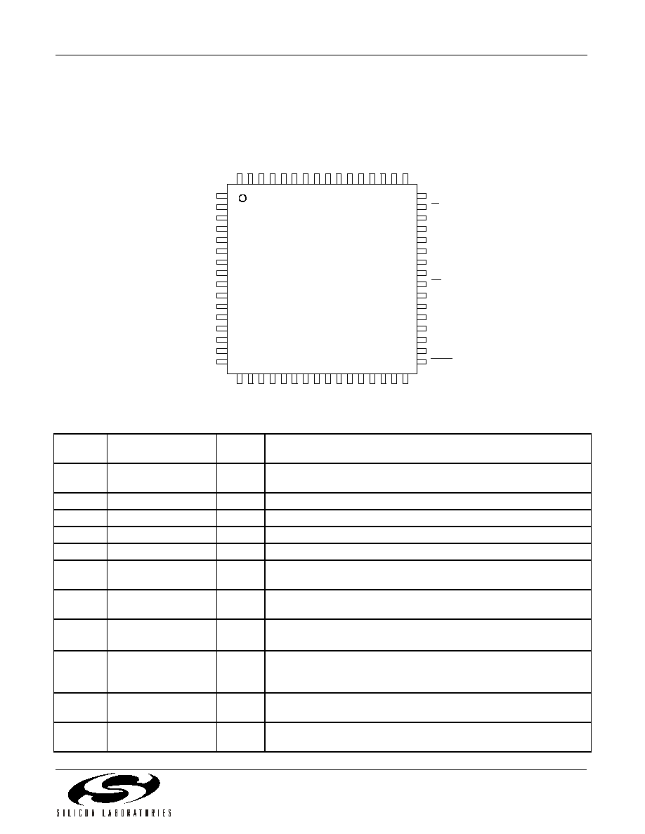
Si3232
Preliminary Rev. 0.96
117
9. Pin Descriptions: Si3232
Pin #(s)
Symbol
Input/
Output
Description
1, 16
SVBATa, SVBATb
I
Battery Sensing Input--
Analog current input used to sense battery
voltage.
2, 15
RPOa, RPOb
O
Transconductance Amplifier Resistor Input Connection.
3, 14
RPIa, RPIb
I
Transconductance Amplifier Resistor Output Connection.
4, 13
RNIa, RNIb
I
Transconductance Amplifier Resistor Output Connection.
5, 12
RNOa, RNOb
O
Transconductance Amplifier Resistor Input Connection.
6, 11
CAPPa, CAPPb
Differential Capacitor--
Capacitor used in low-pass filter to stabilize
SLIC feedback loops.
7, 10
CAPMa, CAPMb
Common Mode Capacitor--
Capacitor used in low-pass filter to sta-
bilize SLIC feedback loops.
8
QGND
Component Reference Ground--
Return path for differential and
common-mode capacitors. Do not connect to system ground.
9
IREF
I
IREF Current Reference--
Connects to an external resistor used to
provide a high-accuracy reference current. Return path for IREF
resistor. Should be routed to QGND pin.
17, 64
STIPDCb, STIPDCa
I
TIP Sense--
Analog current input used to sense dc voltage on TIP
side of subscriber loop.
18, 63
STIPACb,
STIPACa
I
TIP Transmit Input--
Analog input used to sense ac voltage on TIP
side of subscriber loop.
1
2
3
4
5
6
7
8
9
10
11
12
13
14
15
16
48
47
46
45
44
43
42
41
40
39
38
37
36
35
34
33
17
20
19
18
24
23
22
21
31
30
29
28
27
26
25
32
RPIa
SVBATa
RPOa
RNOa
RNIa
CAPPa
CAPMa
QGND
IREF
CAPMb
CAPPb
RNIb
RNOb
RPOb
RPIb
SVBATb
ST
I
P
A
C
b
ST
I
P
D
C
b
SRI
N
G
A
C
b
SRI
N
G
D
Cb
IT
IP
N
b
IRING
N
b
IT
IPP
b
VDD
2
GN
D2
IRING
P
b
TH
E
R
Mb
VC
M
VRXP
b
VRXN
b
VT
XP
b
VT
XN
b
GPOa
SDITHRU
SDI
SDO
SCLK
VDD4
GND4
PCLK
GND3
VDD3
GPOb
BATSELb
FSYNC
ST
I
P
ACa
ST
IP
DCa
SRI
N
G
A
Ca
IT
IP
N
a
IRING
N
a
IT
IP
Pa
VDD
1
GND
1
IRING
P
a
TH
E
R
Ma
VRXN
a
VRXP
a
VT
XP
a
BAT
S
E
L
a
VT
XN
a
RESET
64
61
62
63
57
58
59
60
50
51
52
53
54
55
56
49
CS
INT
SRIN
GDCa
Si3232
64-Lead TQFP
(epad)

Si3232
118
Preliminary Rev. 0.96
19, 62
SRINGACb,
SRINGACa
I
RING Transmit Input--
Analog input used to sense ac voltage on
RING side of subscriber loop.
20, 61
SRINGDCb,
SRINGDCa
I
RING Sense--
Analog current input used to sense dc voltage on
RING side of subscriber loop.
21, 60
ITIPNb, ITIPNa
O
Negative TIP Current Control--
Analog current output providing dc
current return path to V
BAT
from TIP side of the loop.
22, 59
IRINGNb, IRINGNa
O
Negative RING Current Control--
Analog current output providing
dc current return path to V
BAT
from RING side of loop.
23, 58
ITIPPb, ITIPPa
O
Positive TIP Current Control--
Analog current output driving dc cur-
rent onto TIP side of subscriber loop in normal polarity. Also modu-
lates ac current onto TIP side of loop.
24, 37,
42, 57
VDD2, VDD3,
VDD4, VDD1
Supply Voltage--
Power supply for internal analog and digital cir-
cuitry. Connect all VDD pins to the same supply and decouple to
adjacent GND pins as close to the pins as possible.
25, 38,
41, 56
GND2, GND3
GND4, GND1
Ground--
Ground connection for internal analog and digital circuitry.
Connect all pins to low-impedance ground plane.
26, 55
IRINGPb, IRINGPa
O
Positive RING Current Control--
Analog current output driving dc
current onto RING side of subscriber loop in reverse polarity. Also
modulates ac current onto RING side of loop.
27, 54
THERMb, THERMa
I
Temperature Sensor--
Used to sense the internal temperature of
the Si3200. Connect to THERM pin of Si3200 or to V
DD
when using
discrete linefeed circuit.
28
VCM
I
Common Mode Voltage Input
--Connect to external common mode
voltage source.
29, 30
VRXPb, VRXNb
I
Differential Analog Receive Input for SLIC Channel b.
31, 32
VTXPb, VTXNb
O
Differential Analog Transmit Output for SLIC Channel b.
33
RESET
I
Reset--
Active low. Hardware reset used to place all control registers
in known state. An internal pulldown resistor asserts this pin low
when it is not driven externally.
34
FSYNC
I
Frame Sync--
8 kHz frame synchronization signal for internal timing.
May be short or long pulse format.
35, 49
BATSELb, BATSELa
O
Battery Voltage Select Pin--
Used to switch between high and low
external battery supplies.
36, 48
GPOb, GPOa
O
General Purpose Driver Output--
Used to drive test relays for con-
necting loop test equipment or as a second battery select pin.
39
PCLK
I
PCM System Clock--
Master clock input.
40
INT
O
Interrupt--
Maskable interrupt output. Open drain output for wire-
ORed operation.
43
SCLK
I
Serial Port Bit Clock Input--
Controls serial data on SDO and
latches data on SDI.
44
SDO
O
Serial Port Data Out--
Serial port control data output.
45
SDI
I
Serial Port Data In--
Serial port control data input.
Pin #(s)
Symbol
Input/
Output
Description
Si3232
Preliminary Rev. 0.96
119
46
SDITHRU
O
Serial Daisy Chain--
Enables up to 16 devices to use a single CS
for serial port control. Connect SDITHRU pin from master device to
SDI pin of slave device. An internal pullup resistor holds this pin high
during idle periods.
47
CS
I
Chip Select--
Active low. When inactive, SCLK and SDIO are
ignored. When active, serial port is operational.
50, 51
VTXNa, VTXPa
O
Differential Analog Transmit Output for SLIC Channel a.
52, 53
VRXNa, VRXPa
I
Differential Analog Receive Input for SLIC Channel a.
epad
GND
Exposed Die Paddle Ground.
Connect to a low-impedance ground plane via topside PCB pad
directly under the part. See "12. Package Outline: 64-Pin eTQFP" on
page 123 for PCB pad dimensions.
Pin #(s)
Symbol
Input/
Output
Description
Si3232
120
Preliminary Rev. 0.96
10. Pin Descriptions: Si3200
Pin #(s)
Symbol
Input/
Output
Description
1
TIP
I/O
TIP Output
--Connect to the TIP lead of the subscriber loop.
2
NC
No Internal Connection
--Do not connect to any electrical signal.
3
RING
I/O
RING Output
--Connect to the RING lead of the subscriber loop.
4
VBAT
Operating Battery Voltage
--Si3200 internal system battery supply. Con-
nect SVBATa/b pin from Si3232 and decouple with a 0.1
�F/100 V filter
capacitor.
5
VBATH
High Battery Voltage
--Connect to the system ringing battery supply.
Decouple with a 0.1
�F/100 V filter capacitor.
6
VBATL
--
Low Battery Voltage
--Connect to lowest system battery for off-hook oper-
ation driving short loops. An internal diode prevents leakage current when
operating from VBATH.
7
GND
Ground
--Connect to a low-impedance ground plane.
8
VDD
Supply Voltage
--Main power supply for all internal circuitry. Connect to a
3.3 V or 5 V supply. Decouple locally with a 0.1
�F/10 V capacitor.
9
BATSEL
I
Battery Voltage Select
--Connect to the BATSEL pin of the Si3232 through
an external resistor to enable automatic battery switching.
10
NC
No Internal Connection
--Do not connect to any electrical signal.
11
NC
No Internal Connection
--Do not connect to any electrical signal.
12
IRINGN
I
Negative RING Current Control
--Connect to the IRINGN lead of the
Si3232.
13
IRINGP
I
Positive RING Current Drive
--Connect to the IRINGP lead of the Si3232.
14
THERM
O
Thermal Sensor
--Connection to internal temperature-sensing circuit. Con-
nect to THERM pin of Si3232.
Si3200
16-Lead SOIC
(epad)
1
16
2
15
3
14
4
13
5
12
6
11
7
10
8
9
ITIPP
THERM
IRINGP
IRINGN
NC
NC
BATSEL
ITIPN
TIP
NC
RING
VBATH
GND
VBATL
VDD
VBAT
Si3232
Preliminary Rev. 0.96
121
15
ITIPN
I
Negative TIP Current Control
--Connect to the ITIPN lead of the Si3232.
16
ITIPP
I
Positive TIP Current Control
--Connect to the ITIPP lead of the Si3232.
epad
GND
Exposed Die Paddle Ground.
For adequate thermal management, the exposed die paddle should be sol-
dered to a PCB pad that is connected to low-impedance inner and/or back-
side ground planes using multiple vias. See "13. Package Outline: 16-Pin
ESOIC" on page 124 for PCB pad dimensions.
Pin #(s)
Symbol
Input/
Output
Description

Si3232
122
Preliminary Rev. 0.96
11. Ordering Guide
Part Number
Package
Lead Free
Temp Range
Si3232-X-FQ
TQFP-64
Yes
0 to 70 �C
Si3232-X-GQ
TQFP-64
Yes
�40 to 85 �C
Si3200-X-FS
SOIC-16
Yes
0 to 70 �C
Si3200-X-GS
SOIC-16
Yes
�40 to 85 �C
Si3200-KS
SOIC-16
No
0 to 70 �C
Si3200-BS
SOIC-16
No
�40 to 85 �C
Notes:
1. Add an "R" at the end of the device to denote tape and reel option;
2500 quantity per reel.
2. "X" denotes product revision.

Si3232
Preliminary Rev. 0.96
123
12. Package Outline: 64-Pin eTQFP
Figure 39 illustrates the package details for the Si3232. Table 33 lists the values for the dimensions shown in the
illustration.
Figure 39. 64-Pin Thin Quad Flat Package (TQFP)
Table 33. 64-Pin Package Diagram Dimensions
Symbol
Millimeters
Symbol
Millimeters
Min
Nom
Max
Min
Nom
Max
A
--
--
1.20
E
12.00 BSC.
A1
0.05
--
0.15
E1
10.00 BSC.
A2
0.95
1.00
1.05
E2
4.35
4.50
4.65
b
0.17
0.22
0.27
L
0.45
0.60
0.75
c
0.09
--
0.20
aaa
--
--
0.20
D
12.00 BSC.
bbb
--
--
0.20
D1
10.00 BSC.
ccc
--
--
0.08
D2
4.35
4.50
4.65
ddd
--
--
0.08
e
0.50 BSC.
0
�
3.5
�
7
�
Notes:
1. All dimensions shown are in millimeters (mm) unless otherwise noted.
2. Dimensioning and Tolerancing per ANSI Y14.5M-1982.
3. This package outline conforms to JEDEC MS-026, variant ACD-HD.
4. Recommended card reflow profile is per the JEDEC/IPC J-STD-020B specification for Small Body
Components.

Si3232
124
Preliminary Rev. 0.96
13. Package Outline: 16-Pin ESOIC
Figure 40 illustrates the package details for the Si3201. Table 34 lists the values for the dimensions shown in the
illustration.
Figure 40. 16-Pin Thermal Enhanced Small Outline Integrated Circuit (ESOIC) Package
Table 34. Package Diagram Dimensions
Symbol
Millimeters
Min
Max
A
1.35
1.75
A1
0
0.15
B
.33
.51
C
.19
.25
D
9.80
10.00
E
3.80
4.00
e
1.27 BSC
H
5.80
6.20
h
.25
.50
L
.40
1.27
--
0.10
0�
8�
E
H
A1
B
C
h
L
e
See Detail F
Detail F
A
16
9
8
1
D
Seating Plane
Bottom Side
Exposed Pad
2.3 x 3.6 mm
Weight: Approximate device weight is 0.15 grams.
�C�
�A�
�B�
.25 M C A M B S
.25 M B M
x45�

Si3232
Preliminary Rev. 0.96
125
S
UPPORT
D
OCUMENTATION
AN55: Dual ProSLIC User Guide
AN63: Si322x Coefficient Generator User's Guide
AN64: Dual ProSLIC LINC User Guide
AN68: 8-Bit Microcontroller Board Hardware Reference Guide
AN71: Si3220/Si3225 GR-909 testing
AN74: SiLINKPS-EVB User's Guide
AN86: Ringing/Ringtrip Operation and Architecture on the Si3220/Si3225
Si3232PPT0-EVB Data Sheet
Note: Refer to www.silabs.com for a current list of support documents for this chipset.

Si3232
126
Preliminary Rev. 0.96
D
OCUMENT
C
HANGE
L
IST
Revision 0.95 to Revision 0.96
The following changes are specific to Rev G of the
Si3232 silicon:
"4.5.2. Ground Key Detection" on page 34
Added descriptive text and I
LONG
equation.
Register , "ID: Chip Identification (Register Address
0)," on page 67
Added register value for Silicon Rev. G.
The following changes are corrections to Rev 0.96.
Table 34 on page 124.
Corrected 16-pin ESOIC dimension A1.
"4.5.1. Loop Closure Detection" on page 32
Added descriptive text and I
LOOP
equation.
"4.16. SPI Control Interface" on page 50
Added pulldown resistor description
Added description for current limiting resistors on
V
BATH
and V
DD
connected to the Si3200 on page 19.
Revised "2. Typical Application Schematic" on page
17.
Added pulldown resistor to SDO pin.
Added R20�R23, C23, C24, C32, and C33 to V
BATH
and
V
DD
of Si3200.
Updated "11. Ordering Guide" on page 122.
Updated 64-pin eTQFP drawing on page 123.

Si3232
Preliminary Rev. 0.96
127
N
OTES
:

Si3232
128
Preliminary Rev. 0.96
C
ONTACT
I
NFORMATION
Silicon Laboratories Inc.
4635 Boston Lane
Austin, TX 78735
Tel: 1+(512) 416-8500
Fax: 1+(512) 416-9669
Toll Free: 1+(877) 444-3032
Email: ProSLICinfo@silabs.com
Internet: www.silabs.com
Silicon Laboratories, Silicon Labs, and ProSLIC are trademarks of Silicon Laboratories Inc.
Other products or brandnames mentioned herein are trademarks or registered trademarks of their respective holders.
The information in this document is believed to be accurate in all respects at the time of publication but is subject to change without notice.
Silicon Laboratories assumes no responsibility for errors and omissions, and disclaims responsibility for any consequences resulting from
the use of information included herein. Additionally, Silicon Laboratories assumes no responsibility for the functioning of undescribed features
or parameters. Silicon Laboratories reserves the right to make changes without further notice. Silicon Laboratories makes no warranty, rep-
resentation or guarantee regarding the suitability of its products for any particular purpose, nor does Silicon Laboratories assume any liability
arising out of the application or use of any product or circuit, and specifically disclaims any and all liability, including without limitation conse-
quential or incidental damages. Silicon Laboratories products are not designed, intended, or authorized for use in applications intended to
support or sustain life, or for any other application in which the failure of the Silicon Laboratories product could create a situation where per-
sonal injury or death may occur. Should Buyer purchase or use Silicon Laboratories products for any such unintended or unauthorized ap-
plication, Buyer shall indemnify and hold Silicon Laboratories harmless against all claims and damages.