Rev. 0.3 4/06
Copyright © 2006 by Silicon Laboratories
Si8440/1/2
Si8440/1/2
Q
U A D
-C
H A N N E L
D
I G I TA L
I
S O L A T O R
Features
Applications
Safety Regulatory Approvals
Description
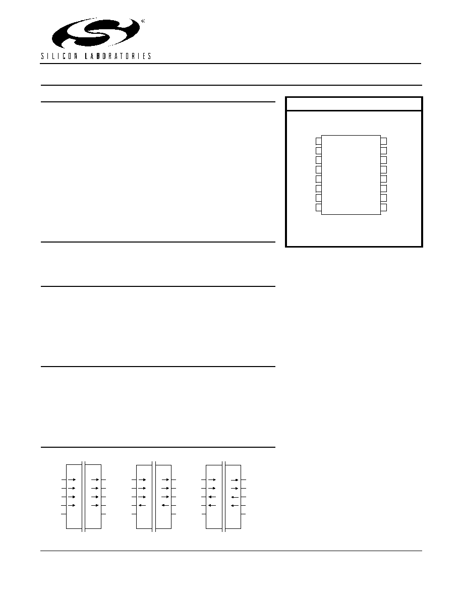
Silicon Lab's family of digital isolators are CMOS devices that employ
an RF coupler to transmit digital information across an isolation
barrier. Very high speed operation at low power levels is achieved.
These parts are available in a 16-pin wide body SOIC package. Three
speed grade options (1, 10, 100 Mbps) are available and achieve
typical propagation delay of less than 10 ns.
Block Diagram
High-speed operation:
DC ≠ 150 Mbps
Low propagation delay:
<10 ns
Wide Operating Supply Voltage:
2.375≠5.5 V
Low power: I1 + I2 <
12 mA/channel at 100 Mbps
Precise timing:
2 ns pulse width distortion
1 ns channel-channel matching
2 ns pulse width skew
2500 V
RMS
isolation
Transient Immunity: >25 kV/µs
Tri-state outputs with ENABLE
control
DC correct
No start-up initialization required
<10 µs Startup Time
High temperature operation:
125 ∞C at 100 Mbps
100 ∞C at 150 Mbps
Wide body SOIC-16 package
Isolated switch mode supplies
Isolated ADC, DAC
Motor control
Power factor correction systems
UL recognition:2500 V
RMS
for 1
Minute per UL1577
CSA component acceptance
notice #5A
* All Pending
VDE certification conformity
DIN EN 60747-5-2 (VDE0884
Part 2):2003-01
DIN EN60950(VDE0805):
2001-12;EN60950:2000
V
IORM
= 560 V
PEAK
Si8441
Si8442
B1
A1
A3
A4
A2
B3
B4
B2
Si8440
A1
A3
A4
A2
B3
B4
B2
B1
A1
A3
A4
A2
B3
B4
B2
B1
NC
EN1
EN1
EN2
EN2
EN2
Pin Assignments
Wide Body SOIC
V
DD1
GND1
A1
A3
A4
EN1
GND1
A2
1
2
3
4
5
6
7
8
Top View
V
DD2
GND2
B2
B1
B4
B3
GND2
EN2
9
12
11
10
13
14
15
16

Si8440/1/2
Rev. 0.3
3
T
A B L E
O F
C
O N T E N TS
Section
Page
1. Electrical Specifications . . . . . . . . . . . . . . . . . . . . . . . . . . . . . . . . . . . . . . . . . . . . . . . . . . .4
2. Typical Performance Characteristics . . . . . . . . . . . . . . . . . . . . . . . . . . . . . . . . . . . . . . . .13
3. Application Information . . . . . . . . . . . . . . . . . . . . . . . . . . . . . . . . . . . . . . . . . . . . . . . . . . .15
3.1. Theory of Operation . . . . . . . . . . . . . . . . . . . . . . . . . . . . . . . . . . . . . . . . . . . . . . . . .15
3.2. Eye Diagram . . . . . . . . . . . . . . . . . . . . . . . . . . . . . . . . . . . . . . . . . . . . . . . . . . . . . . .15
4. Layout Recommendations . . . . . . . . . . . . . . . . . . . . . . . . . . . . . . . . . . . . . . . . . . . . . . . .16
4.1. Supply Bypass . . . . . . . . . . . . . . . . . . . . . . . . . . . . . . . . . . . . . . . . . . . . . . . . . . . . .16
4.2. Input and Output Characteristics . . . . . . . . . . . . . . . . . . . . . . . . . . . . . . . . . . . . . . . .16
4.3. Enable Inputs . . . . . . . . . . . . . . . . . . . . . . . . . . . . . . . . . . . . . . . . . . . . . . . . . . . . . .16
4.4. RF Immunity and Common Mode Transient Immunity . . . . . . . . . . . . . . . . . . . . . . .17
4.5. RF Radiated Emissions . . . . . . . . . . . . . . . . . . . . . . . . . . . . . . . . . . . . . . . . . . . . . . .18
5. Pin Descriptions . . . . . . . . . . . . . . . . . . . . . . . . . . . . . . . . . . . . . . . . . . . . . . . . . . . . . . . . .19
6. Ordering Guide . . . . . . . . . . . . . . . . . . . . . . . . . . . . . . . . . . . . . . . . . . . . . . . . . . . . . . . . . .20
7. Package Outline: Wide Body SOIC . . . . . . . . . . . . . . . . . . . . . . . . . . . . . . . . . . . . . . . . . .21
Document Change List . . . . . . . . . . . . . . . . . . . . . . . . . . . . . . . . . . . . . . . . . . . . . . . . . . . . .22
Contact Information . . . . . . . . . . . . . . . . . . . . . . . . . . . . . . . . . . . . . . . . . . . . . . . . . . . . . . . .24
Si8440/1/2
4
Rev. 0.3
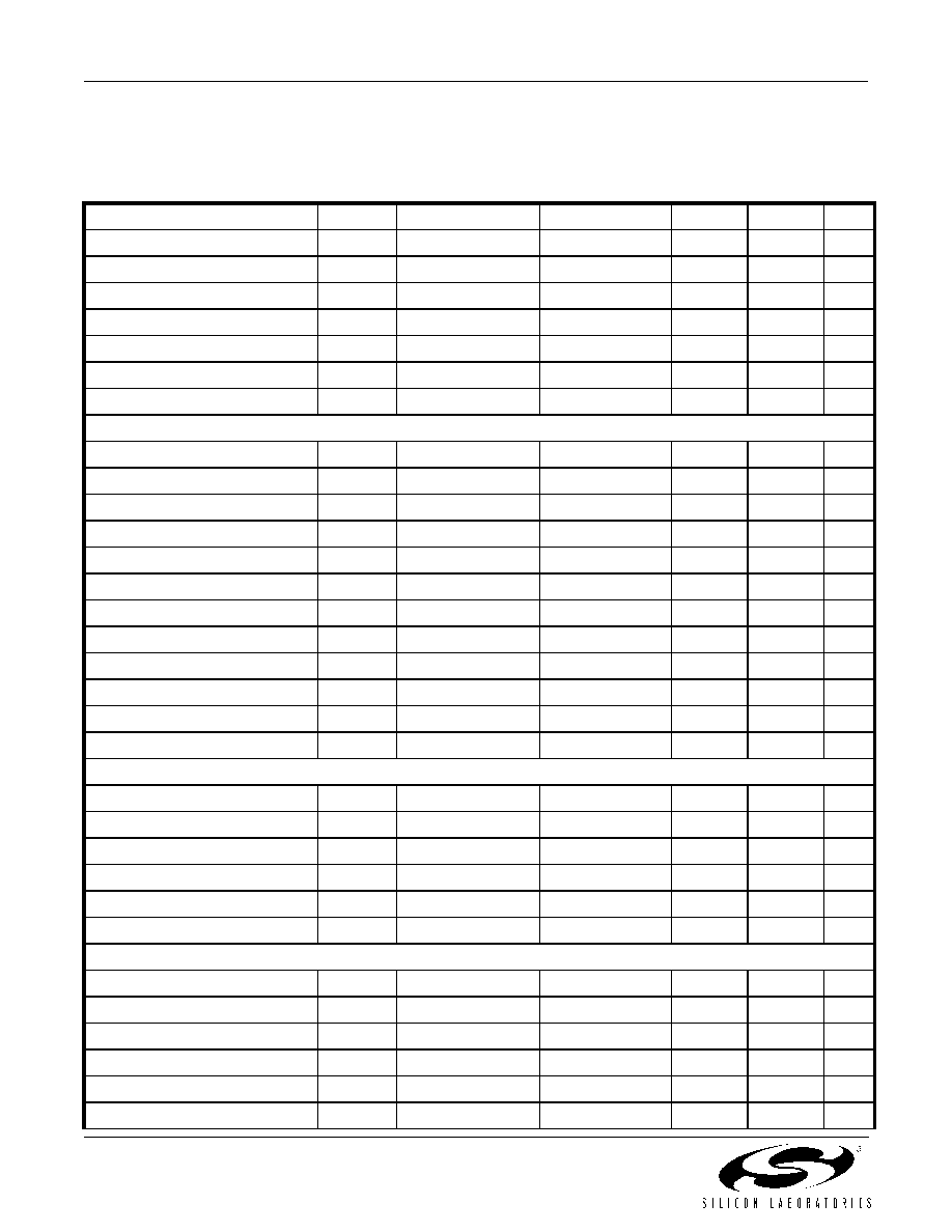
1. Electrical Specifications
Table 1. Electrical Characteristics
(V
DD1
= 5 V, V
DD2
= 5 V, T
A
= ≠40 to 125 C∞)
Parameter
Symbol
Test Condition
Min
Typ
Max
Unit
High Level Input Voltage
V
IH
2.0
--
--
V
Low Level Input Voltage
V
IL
--
--
0.8
V
High Level Output Voltage
V
OH
loh = ≠4 mA
V
DD1
,V
DD2
≠ 0.4
4.8
--
V
Low Level Output Voltage
V
OL
lol = 4 mA
--
0.2
0.4
V
Input Leakage Current
I
L
--
--
±10
µA
Enable Input High Current
I
ENH
V
ENx
= V
IH
--
4
--
µA
Enable Input Low Current
I
ENL
V
ENx
= V
IL
--
20
--
µA
DC Supply Current (All inputs 0 V or at Supply)
Si8440-A,-B,-C, V
DD1
All inputs 0 DC
--
7.5
--
mA
Si8440-A,-B,-C, V
DD2
All inputs 0 DC
--
7
--
mA
Si8440-A,-B,-C, V
DD1
All inputs 1 DC
--
15
--
mA
Si8440-A,-B,-C, V
DD2
All inputs 1 DC
--
6.5
--
mA
Si8441-A,-B,-C, V
DD1
All inputs 0 DC
--
8.7
--
mA
Si8441-A,-B,-C, V
DD2
All inputs 0 DC
--
11
--
mA
Si8441-A,-B,-C, V
DD1
All inputs 1 DC
--
14
--
mA
Si8441-A,-B,-C, V
DD2
All inputs 1 DC
--
12.5
--
mA
Si8442-A,-B,-C, V
DD1
All inputs 0 DC
--
10
--
mA
Si8442-A,-B,-C, V
DD2
All inputs 0 DC
--
10
--
mA
Si8442-A,-B,-C, V
DD1
All inputs 1 DC
--
13
--
mA
Si8442-A,-B,-C, V
DD2
All inputs 1 DC
--
13
--
mA
10 Mbps Supply Current (All inputs = 5 MHz square wave, CI = 15 pF on all outputs)
Si8440-B,-C, V
DD1
--
11
--
mA
Si8440-B,-C, V
DD2
--
9
--
mA
Si8441-B,-C, V
DD1
--
12
--
mA
Si8441-B,-C, V
DD2
--
13.5
--
mA
Si8442-B,-C, V
DD1
--
12.5
--
mA
Si8442-B,-C, V
DD2
--
12.5
--
mA
100 Mbps Supply Current (All inputs = 50 MHz square wave, CI = 15 pF on all outputs)
Si8440-C, V
DD1
--
12
--
mA
Si8440-C, V
DD2
--
27
--
mA
Si8441-C, V
DD1
--
16
--
mA
Si8441-C, V
DD2
--
27
--
mA
Si8442-C, V
DD1
--
21
--
mA
Si8442-C, V
DD2
--
21
--
mA
Si8440/1/2
Rev. 0.3
5
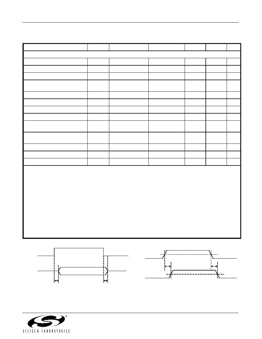
Timing Characteristics
Maximum Data Rate
0
--
100
Mbps
Minimum Pulse Width
--
5
--
ns
Propagation Delay
1
t
PHL
, t
PLH
--
7.5
--
ns
Pulse Width Distortion
|t
PLH
-
t
PHL
|
1
PWD
--
1
--
ns
Propagation Delay Skew
2
t
PSK
--
6
--
ns
Channel-Channel Skew
3
t
PSKCD/OD
--
0.5
--
ns
Output Rise Time
C1 = 15 pF
--
2
--
ns
Output Fall Time
C1 = 15 pF
--
2
--
ns
Common Mode Transient
Immunity at Logic Low Output
4
CM
L
25
30
--
kV/µs
Common Mode Transient
Immunity at Logic High Output
4
CM
H
25
30
--
kV/µs
Enable to Data Valid
t
en1
--
5
--
ns
Enable to Data Tri-State
t
en2
--
5
--
ns
Start-up Time
5
t
SU
--
3
--
µs
Notes:
1. t
PHL
propagation delay is measured from the 50% level of the falling edge of the V
Ix
signal to the 50% level of the falling
edge of the V
Ox
signal. t
PLH
propagation delay is measured from the 50% level of the rising edge of the V
Ix
signal to the
50% level of the rising edge of the V
Ox
signal.
2. t
PSK
is the magnitude of the worst-case difference in t
PHL
or t
PLH
that is measured between units at the same operating
temperature, supply voltages, and output load within the recommended operating conditions.
3. Codirectional channel-to-channel matching is the absolute value of the difference in propagation delays between any
two channels with inputs on the same side of the isolation barrier. Opposing-directional channel-to-channel matching is
the absolute value of the difference in propagation delays between any two channels with inputs on opposing sides of
the isolation barrier.
4. CM
H
is the maximum common-mode voltage slew rate that can be sustained while maintaining V
O
> 0.8 V
DD2
. CM
L
is
the maximum common-mode voltage slew rate that can be sustained while maintaining V
O
< 0.8 V. The common-mode
voltage slew rates apply to both rising and falling common-mode voltage edges. The transient magnitude is the range
over which the common mode is slewed.
5. Start-up time is the time period from the application of power to valid data at the output.
Table 1. Electrical Characteristics (Continued)
(V
DD1
= 5 V, V
DD2
= 5 V, T
A
= ≠40 to 125 C∞)
Parameter
Symbol
Test Condition
Min
Typ
Max
Unit
Figure 1. ENABLE Timing Diagram
Figure 2. Propagation Delay Timing
ENABLE
OUTPUTS
t
en1
t
en2
INPUT
(V
IX
)
OUTPUT
(V
OX
)
t
PLH
t
PHL
50%
50%
