 | –≠–ª–µ–∫—Ç—Ä–æ–Ω–Ω—ã–π –∫–æ–º–ø–æ–Ω–µ–Ω—Ç: SC9102C | –°–∫–∞—á–∞—Ç—å:  PDF PDF  ZIP ZIP |


Silan
Semiconductors
SC9102C/D
HANGZHOU SILAN MICROELECTRONICS CO.,LTD.
Rev: 2.0
2001-11-02
3
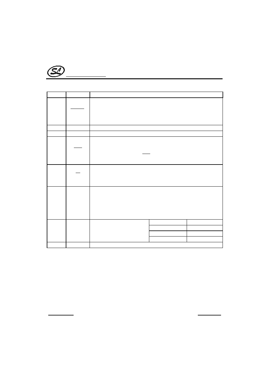
ABSOLUTE MAXIMUM RATINGS
(Tamb=25
∞
C, All voltage referenced to Vss, unless otherwise specified)
Characteristic
Symbol Value
Unit
Power Supply Voltage
V
DD
6.0
V
Input Voltage
V
IN
-0.3~V
DD
+0.3
V
Power Dissipation
P
D
500
mW
Operating Temperature
Topr
-25~+70
∞
C
Storage Temperature
Tstg
-55~+150
∞
C
ELECTRICAL CHARACTERISTICS
(Tamb=25
∞
C , V
DD
=2.5V, fosc=3.579545MHz, unless otherwise specified)
Parameter Symbo
l
Conditions
Min
Typ
Max
Unit
Tone/Pulse
2.0
5.5
Operating Voltage
V
DD
Memory retension
1.0
5.5
V
Tone
0.6
2
Operating Current
I
OP
Pulse, OFF-HOOK, Keypad
entry, no load
0.2
0.6
mA
Standby Current
I
S
ON-HOOK
No keypad
entry ,no load V
DD
=1.0V
0.1
5
µ
A
Memory Retension Current
Imr
0.1
0.1
µ
A
Control Pin Input Low Voltage
Vil
VSS
0.3V
DD
Control Pin Input High Voltage
Vih
0.7V
DD
V
DD
V
XMUTE Pin Leakage Current
Imth
V
XMUTE
=12.0V
1
µ
A
XMUTE Pin Sink Current
Imtl
V
XMUTE
=0.5V
1
mA
HKS Pin Input Current
Ihks
Vhks=2.5V
0.1
µ
A
Drive Current
Ikbd
Vn=0V
note1
4
10
30
Keyboard
Scanning Pin
Sink Current
Ikbs
Vn=2.5
note1
200
400
µ
A
Key-in Debounce Time
t
DB
20
ms
Pulse Mode
Pulse Output Pin Leakage Current
Ipoh
Vpo=12V
--
--
1.0
µ
A
Pulse Output Pin Sink Current
Ipol
Vpo=0.5V
1. 0
3.0
--
mA
--
10
--
Pulse Rate
fpr
--
20
--
pps
--
40:60
--
Make/Break Ratio
t
M
t
B
--
33:66
--
%
(to be continued)

Silan
Semiconductors
SC9102C/D
HANGZHOU SILAN MICROELECTRONICS CO.,LTD.
Rev: 2.0
2001-11-02
4
(continued)
Parameter Symbol
Conditions
Min
Typ
Max
Unit
M/B ratio=40:60
--
40
--
Pre-digit Pause
Pulse rate=10pps
t
PDP
M/B ratio=33:66
--
33
--
ms
M/B ratio=40:60
--
20
--
Pre-digit Pause
Pulse rate=20pps
t
PDP
M/B ratio =33:66
--
16.5
--
ms
Pulse rate=10pps
--
800
--
Inter-digit Pause
t
IDP
Pulse rate=20pps
--
600
--
ms
Tone Mode
DC Level
Vdc
V
DD
=2.0V~5.5V
0.45V
DD
0.55V
DD
0.7V
DD
V
Sink Current
Itl
Vdtmf=0.5V
0.15
--
--
mA
AC level
Vdtmf
Row group
R
L
=10K
120
150
180
mVrms
Tone
Output Pin
Load Resistor
R1
Dist.<=-23dB
10
--
--
K
Pre-emphasis
twist
V
DD
=2.0~5.5 V
1
2
3
dB
DTMF Signal
Distortion(note 2)
Dist.
R
L
=10K
--
-30
-23
dB
Minimum tone duration Time
t
TD
Auto redial
--
100
--
ms
Minimum Intertone Pause Time
t
TTP
Auto redial
--
106
--
ms
Note: 1. Vn: Input voltage of any keyboard scanning pin (Row group, Column group)
2
Distortion (dB) = 20log
{[
V
1
2
+V
2
2
+V
3
2
+...Vn
2
)
1/2
]
/
[
(V
L
2
+V
H
2
)
1/2
]}
V
L
,V
H
: Row group and Column group signal
V1
V2...
Vn: Harmonic signal (BW = 300Hz~3500Hz
ACTUAL FREQUENCY OUTPUT
(fosc=3.579545MHz)
Keyboard Scanning Pin
Standard(Hz)
Output
Deviation(%)
R1
f1
697
699
+0.28
R2
f2
770
766
-0.52
R3
f3
852
848
-0.47
R4
f4
941
948
+0.74
C1
f5
1209
1216
+0.57
C2
f6
1336
1332
-0.30
C3
f7
1477
1472
-0.34

Silan
Semiconductors
SC9102C/D
HANGZHOU SILAN MICROELECTRONICS CO.,LTD.
Rev: 2.0
2001-11-02
5
PIN DESCRIPTION
Pin No.
Pin Name
Description
15
C1
16
C2
17
C3
18
C4
1
R1
2
R2
3
R3
4
R4
*Provides keyboard scanning.
* HKS pin is LOW, the column group stays in "HIGH" and row group stays in "LOW"
state.
*The keypad is compatible with the standard dual contact matrix keyboard (as
figure1b), the inexpensive single contact keyboard (as figure 1a), and electronic input
(as figure 1c).
*When HKS is "LOW", a valid key entry is defined by related Row & Column
connection or by electronic input.
*Activation of two or more keys will result in no response, except for single key.
*To avoid keyboard-bouncing error, this chip provides built-in debounce circuit. (The
debounce time = 20ms)
V
DD
Column
Row
Column
Row
Column
V
SS
V
DD
V
SS
Row
Figure1a: Single contact form
keyboard configuration
Figure1b: Dual contact form
keyboard configuration
Figure1c: Electronic signal input keyboard configuration
8
OSCI
9
OSCO
*Oscillator input & output pins.
*The 3.579545MHz oscillator is formed by a built-in inverter inside of this chip and by
connecting a 3.579545MHz crystal or a ceramic resonator across the OSCI and
OSCO pins. (built-in feedback resistor and capacitor)
*When HKS is "LOW", a valid key-in may turn on this oscillator and generates a
3.579545 MHz clock.
(to be continued)
Silan
Semiconductors
SC9102C/D
HANGZHOU SILAN MICROELECTRONICS CO.,LTD.
Rev: 2.0
2001-11-02
6
(continued)
Pin No.
Pin Name
Description
13
XMUTE
*Mute output pins.
*NMOS open drain output structure.
*The output is in "LOW" state during dialing sequence (both Pulse and Tone mode)
otherwise this pin is "high-impedance".
*Long (continue) Mute.
11
VSS
*Negative power supply pin.
10
VDD
*Positive power supply pin.
5
HKS
*Hook switch input pin.
*When the handset is in ON-HOOK state, this pin must be pulled "high" in order to
disable the dialing operation and decrease the power consumption.
*When in OFF-HOOK state, the
HKS
pin must be pulled "low" state for all function
operation.
14
PO
*Pulse output signal pin.
*NMOS open drain output structure.
*The output is "LOW" during pulse dialing and Flash operation, otherwise this output
is "floating".
12
TONE
*Dual Tone Multi-frequency output pin.
*In TONE mode, when an entry of digit key (include *, # key), this pin will send out a
corresponding DTMF signal.
*The TONE pin provides minimum tone duration and minimum intertone pause time
to support rapid key-in. If key-in time is less than 100ms, DTMF signal will last for
100ms; otherwise the tone duration will last as long as the key is pressed.
MODE Dialing
mode
V
DD
Pulse mode
Open
Pulse mode
7
MODE
*Mode selection pin.
*Three-state input structure.
*This pin can select the three
modes shown on the right.
V
SS
Tone mode
6
M/B
*M/B ration selection pin. (The function seeing the Dialing signal option table)

Silan
Semiconductors
SC9102C/D
HANGZHOU SILAN MICROELECTRONICS CO.,LTD.
Rev: 2.0
2001-11-02
7
KEYBOARD OPERATION
Symbol definitions:
a)
:
OFF-HOOK or enable Hand Free function.
b)
:
ON-HOOK or disable Hand Free function.
c)
:
Input level from low to high.
d)
:
Input level from high to low.
e)
D1~Dn
:
Digit key
1, 2, 3, 4, 5, 6, 7, 8, 9, 0, *, #, (C1~Cn is same as D1~Dn).
f)
Dp1~Dpn
:
Pulse digit
1, 2, 3, 4, 5, 6, 7, 8, 9, 0, *, #, (Cp1~Cpn is same as Dp1~Dpn).
g)
Dt1~Dtn
:
Tone digit
1, 2, 3, 4, 5, 6, 7, 8, 9, 0, *, #, (Ct1~Ctn is same as Dt1~Dtn).
h)
t
F
:
Flash time.
i)
t
P
:
Pause time.
j)
t
PT
:
Pulse to Tone wait time.
k)
t
FP
:
Pause time for flash.
l)
t
RP
:
Pause time for redial.
m)
LNB
:
Last number redial buffer.
A
Normal Dialing
1. Digit Dialing
Procedure
D1, D2..., Dn
Dial out
Dt1, Dt2..., Dtn (in Tone mode)
Dial out
Dp1, Dp2,..., Dpn (in Pulse mode)
LNB
D1, D2..., Dn
2. Dialing with flash key
Procedure
F, D1, D2..., Dn
Dial out
t
F
, t
FP
, Dt1, Dt2..., Dtn (in Tone mode)
Dial out
t
F
, t
FP
, Dp1, Dp2, ..., Dpn (in Pulse mode)
LNB
D1, D2..., Dn
3. Dialing with P
T key
Procedure
D1, D2 ..., P
T , ..., Dn
Dial out
Dp1, Dp2, ..., t
PT
, ..., Dpn (in Pulse mode)
LNB
D1, D2 ..., P
T , ..., Dn
Note: If key in digit over maximum digit stored in LNB, then RD is inhibit even after on/off hook.

Silan
Semiconductors
SC9102C/D
HANGZHOU SILAN MICROELECTRONICS CO.,LTD.
Rev: 2.0
2001-11-02
8
B
Mixed dialing
Procedure
D1, D2..., P
T , D9, D10 ..., Dn
Dial out
Dp1, Dp2, ..., t
PT
, Dt9, Dt10..., Dtn
LNB
D1, D2..., P
T , D9, D10 ..., Dn
C
Redial
LNB
D1, D2..., Dn
Procedure
RD
Dial out
t
RP
, Dt1, Dt2..., Dtn (in Tone mode)
Dial out
t
RP
, Dp1, Dp2,..., Dpn (in Pulse mode)
Note: If key in digit over maximum digit stored in LNB, then RD is inhibit.
D
Pause Function
Procedure
D1, D2..., Dn, P, C1 ..., Cn
Dial out
Dt1, Dt2 ,..., Dtn , t
P
, Ct1 ..., Ctn (in Tone mode)
Dial out
Dp1, Dp2, ..., Dpn , t
P
, Cp1 ..., Cpn (in Pulse mode)
LNB
D1, D2..., Dn, P , C1, C2 ..., Cn
E
Flash Function
Procedure
D1, D2..., Dn, F, C1 ..., Cn
Dial out
Dt1, Dt2,..., Dtn , t
F
, t
FP
, Ct1 ..., Ctn (in Tone mode)
Dial out
Dp1, Dp2,..., Dpn , t
F
, t
FP
, Cp1 ..., Cpn (in Pulse mode)
LNB
C1, C2 ..., Cn

Silan
Semiconductors
SC9102C/D
HANGZHOU SILAN MICROELECTRONICS CO.,LTD.
Rev: 2.0
2001-11-02
9
TEST CIRCUIT
A
HKS
V
SS
MODE
V
DD
DP
DP
DT
keyboard
Operation
current
1
2
Standby
current
V+
Tone output voltage
3
Tone distortion
4
keyboard
HKS
V
SS
TONE
V
DD
V+
keyboard
counter
and
AC meter
10K
HKS
V
SS
TONE
V
DD
V+
Spectrum
analyzer
V
10K
A
HKS
V
DD
V
SS
V+
HKS V
SS
R*
V
DD
Keypad input current (row group)
7
V+
C*
ROW
MODE
A
Pulse output sink current
(open drain structure)
5
6
Pulse output sink current
(inverter structure)
8
HKS V
SS
R*
V
DD
V+
C*
COLUMN
MODE
A
PO
Flash
key
HKS
V
SS
V
DD
V+
V
VEXT
A
PO
V
SS
V
DD
V+
HKS
V
VEXT
A
keypad input current (column group)
Note: 1. Dist. (dB)=20log
{[
V
1
2
+V
2
2
+V
3
2
+...V
n
2
)
1/2
]
/
[
(V
L
2
+V
H
2
)
1/2
]}
a. V1...Vn are extraneous frequencies (ie, inter modulation and harmonic), components in the 500Hz to 3400Hz band.
b. V
L
,V
H
are the individual frequency components of DTMF signal.
c. Whether keyboard is pushed refer to the TONE mode time diagram.
2. Sink current Isink=I/(1-Duty Cycle), I is the net DC current measured from ampere meter.

Silan
Semiconductors
SC9102C/D
HANGZHOU SILAN MICROELECTRONICS CO.,LTD.
Rev: 2.0
2001-11-02
10
3. R*, C* mean other column and row.
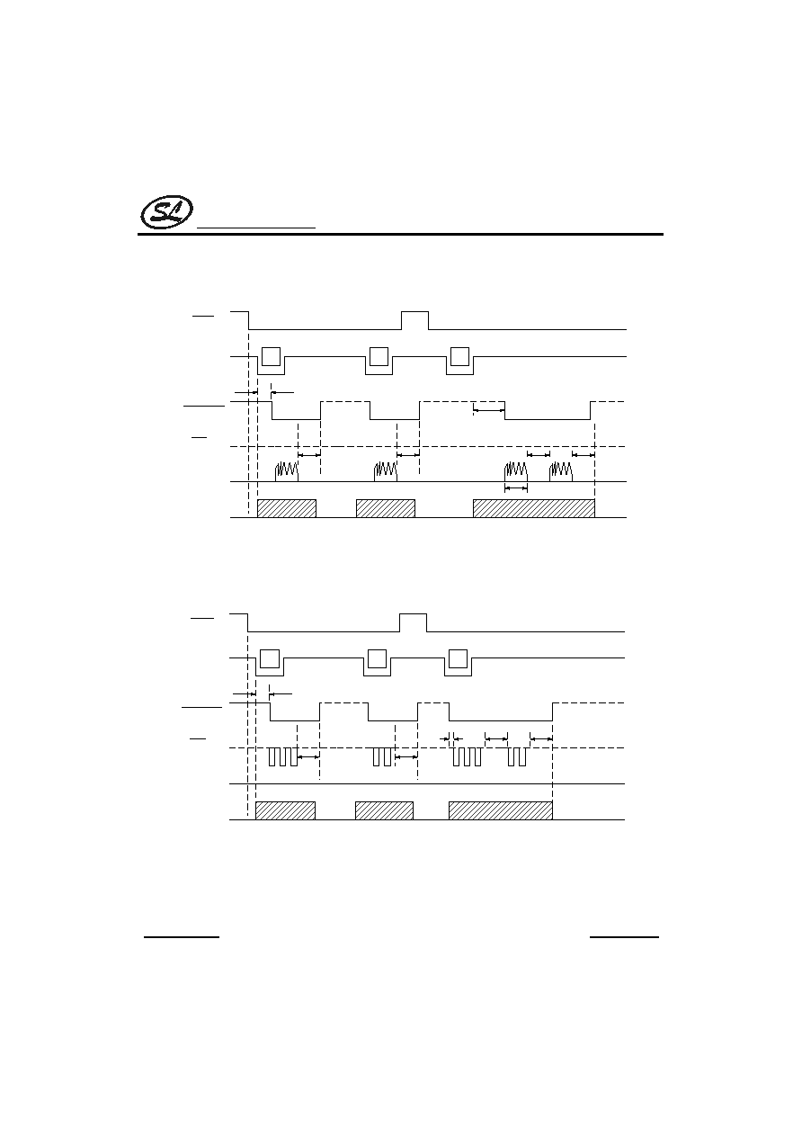
TIMING DIAGRAMS
3
2
3
HKS
KEY IN
XMUTE
PO
TONE
OSCO
t
TD
t
ITP
t
ITP
Normal dialing
......High impedance
t
DB
t
ITP
Tone Mode Timming Diagram
3
2
3
HKS
KEY IN
XMUTE
PO
TONE
OSCO
t
TD
t
IDP
t
IDP
Normal dialing
......High impedance
t
DB
t
PDP
t
B
t
M
t
IDP
Pusle Mode Timming Diagram

Silan
Semiconductors
SC9102C/D
HANGZHOU SILAN MICROELECTRONICS CO.,LTD.
Rev: 2.0
2001-11-02
11
TIMING DIAGRAMS
(continued)
3
2
3
HKS
KEY IN
XMUTE
PO
TONE
OSCO
t
TD
t
ITP
t
ITP
......High impedance
t
DB
t
ITP
P
T
t
PDP
t
PT
Timming Waveform for mixed dialing Operation
(by */T key entry)
3
2
3
HKS
KEY IN
XMUTE
PO
TONE
OSCO
t
IDP
t
IDP
......High impedance
t
DB
t
PDP
t
IDP
MODE
Timming Waveform for mixed dialing Operation
(by MODE pin entry)
Silan
Semiconductors
SC9102C/D
HANGZHOU SILAN MICROELECTRONICS CO.,LTD.
Rev: 2.0
2001-11-02
12
TIMING DIAGRAMS
(continued)
3
RD
HKS
KEY IN
XMUTE
PO
TONE
OSCO
......High impedance
t
DB
2
t
ITP
t
ITP
t
ITP
t
TD
t
ITP
t
RP
Tone Mode Redial Timming Diagram
3
RD
HKS
KEY IN
XMUTE
PO
TONE
OSCO
......High impedance
t
DB
2
t
IDP
t
IDP
t
IDP
t
IDP
t
RP
Pulse Mode Redial Timming Diagram

Silan
Semiconductors
SC9102C/D
HANGZHOU SILAN MICROELECTRONICS CO.,LTD.
Rev: 2.0
2001-11-02
13
TIMING DIAGRAMS
(continued)
XMUTE
PO
TONE
OSCO
......High impendance
t
DB
t
ITP
t
P
t
ITP
3
3
HKS
KEY IN
XMUTE
PO
TONE
OSCO
t
DB
P
t
PDP
t
IDP
2
t
IDP
t
IDP
t
P
t
ITP
Pause key operating timming
3
HKS
KEY IN
XMUTE
PO
TONE
OSCO
t
DB
t
F
t
FP
......High impedance
Flash key operating timming

Silan
Semiconductors
SC9102C/D
HANGZHOU SILAN MICROELECTRONICS CO.,LTD.
Rev: 2.0
2001-11-02
14
TYPACAL APPLICATION CIRCUIT
SC9102C/D
1
2
3
4
P
T
F
P
RD
3
6
9
#/RD
2
5
8
0
1
4
7
*/P
18
17
16
15
11
7
6
14
10
5
12
8
9
13
2-4
Speech
network
R1
R2
R3
R4
PO
C4
C3
C2
C1 V
SS
MODE
M/B
XMUTE
V
DD
TONE
HKS
OSCI
OSCO
100k
3.3k
100k
100k
22M
A92
A42
5V
100
µ
F
1N
4148x
2
2.2k
220k
100k
1
µ
F
220k
ON/OFF
HOOK
Tip
Ring
1N4148x4
1.5k
200
C945
0.02
µ
F
C945
3.579545MHz
DP
DP
DT
33.3/66.6 10pps
40/60
10pps
33.3/66.6 20pps
1000pF
ZNR
120V
V
DD
V
DD
V
DD

Silan
Semiconductors
SC9102C/D
HANGZHOU SILAN MICROELECTRONICS CO.,LTD.
Rev: 2.0
2001-11-02
15
CHIP TOPOGRAPHY
12
11
10
9
8
7
6
5
4
3
2
1
18
17
16
15
14
13
Chip size: 1.35 x 1.33 mm
2
PAD COORDINATES
(Unit:
µ
m)
Pad No.
Symbol
X
Y
Pad No.
Symbol
X
Y
1
P1
-545.0
276.0
10
P10
542.2
176.4
2
P2
-545.0
109.0
11
P11
541.3
349.5
3
P3
-539.0
-266.0
12
P12
541.0
530.5
4
P4
539.0
-453.5
13
P13
324.3
531.5
5
P5
21.2
-528.0
14
P14
131.0
533.0
6
P6
191.0
-528.0
15
P15
-27.0
531.5
7
P7
362.5
-381.5
16
P16
-199.5
531.5
8
P8
529.5
8.5
17
P17
-373.0
531.5
9
P9
540.5
176.4
18
P18
-545.0
463.5
Note: The original point of the coordinate is the die center.
Silan
Semiconductors
SC9102C/D
HANGZHOU SILAN MICROELECTRONICS CO.,LTD.
Rev: 2.0
2001-11-02
16
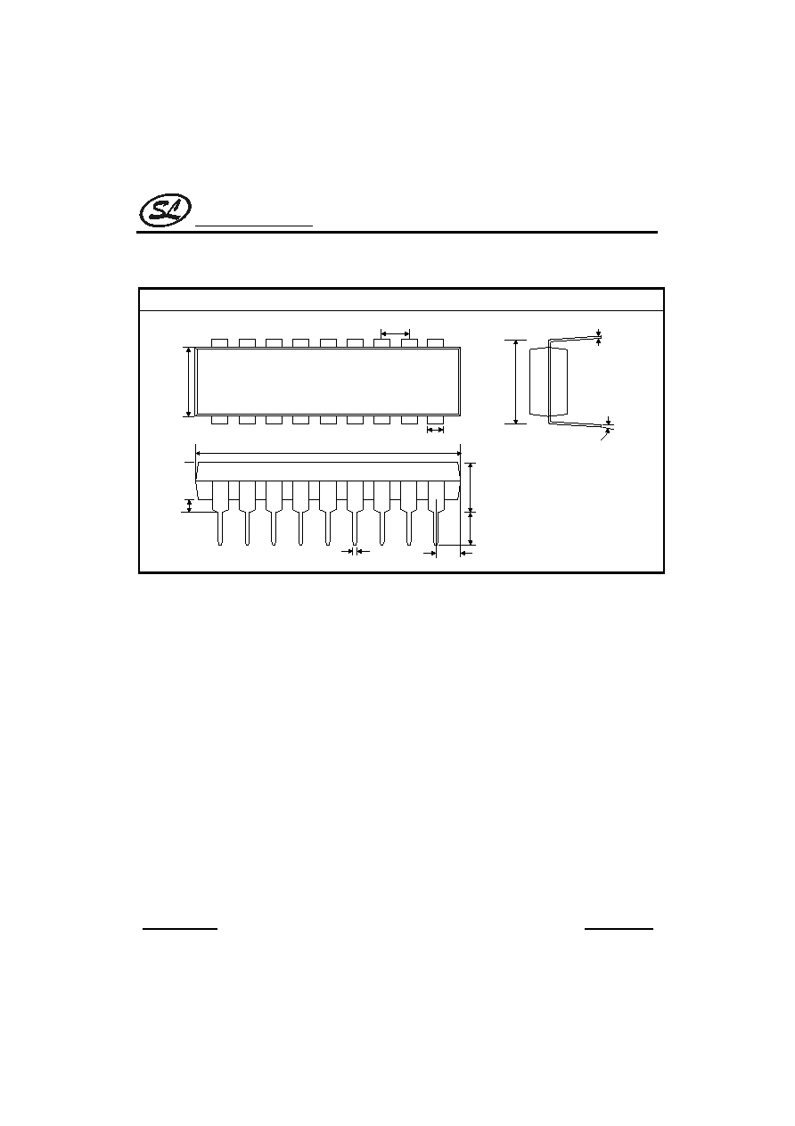
PACKAGE OUTLINE
DIP-18-300-2.54
UNIT: mm
6.
40
B
0.
25
2.54
0.5MIN
4.
36M
A
X
3.
00M
I
N
0.46
B
0.08
23.12
B
0.3
1.52
7.
62
0.
25
B
0.
05
15 Degree
1.27MAX
+0.3
-0