
Silan
Semiconductors
SC9149A/SC9150A
HANGZHOU SILAN MICROELECTRONICS CO.,LTD.
Rev: 1.2 2003.01.21
1
INFRARED REMOTE CONTROL
RECEIVER
DESCRIPTION
The SC9149A/SC9150A are CMOS LSIs designed for use on the
infrared remote control receiver, and when this LSI is used in
combination with SC9148A for transmitter, the remote control
system can be constructed. The SC9149A is DIP-16 type and is
capable of controlling 10 functions, while the SC9150A is DIP-24
type and is capable of controlling 18 functions.
FEATURES
* Able to output parallel multiple keying signals sent from the
transmitter (The SC9149A is able to output parallel up to 5
functions, while the SC9150A is able to output parallel up to 6
functions.)
* Output for single pulse, hold pulse and cyclic pulse are provided.
(cyclic pulse is available only for SC9150A)
* A single terminal type oscillator by means of CR is provided.
* Code detection circuit provided for code check with the
transmitter prevents inter-ferences from various types of
machines and apparatus.
SDIP-24
DIP-16
SC9149A
SC9150A
ORDERING INFORMATION
SC9149A
Advanced version DIP-16 package
SC9149AL
Advanced Dependent cyclic (toggle) Outputs
SC9149AHN
Inversed Rxin input
Output format same as "L", except that when HP1 or HP2 is active, it will clear CP1.
SC9150A
Advanced version DIP-24 package
PIN CONFIGURATION
SC9149AL/
9149AHN
15
16
14
12
13
11
10
9
2
1
3
5
4
6
7
8
GND
Rx IN
HP1
HP2
HP3
HP4
HP5
CP2
CP1
SP3
SP2
SP1
CODE 3
CODE 2
OSC
VDD
SC9149A
15
16
14
12
13
11
10
9
2
1
3
5
4
6
7
8
GND
Rx IN
HP1
HP2
HP3
HP4
HP5
SP5
SP4
SP3
SP2
SP1
CODE 3
CODE 2
OSC
VDD
SC9150A
15
16
14
12
13
2
1
3
5
4
6
7
8
9
10
11
19
20
18
17
23
24
22
21
GND
Rx IN
HP1
HP2
HP3
HP4
HP5
HP6
CP2
CP1
SP10
SP9
SP8
SP7
SP6
SP5
SP4
SP3
SP2
SP1
CODE 2
CODE 1
OSC
VDD
Silan
Semiconductors
SC9149A/SC9150A
HANGZHOU SILAN MICROELECTRONICS CO.,LTD.
Rev: 1.2 2003.01.21
2
BLOCK DIAGRAM
Input shift
register
Input Pulse
counter
Shift register
Data Check
Latch Circuit
Output Buffer
Code
Check
Error
Detection
F/F
F/F
Up Counter
OSC
11
12
13
14
15
2
1
16
10
9
8
7
6
5
4
3
VDD
OSC
CODE 2 CODE 3
SP1
SP2
SP3
SP4
SP5
HP1
HP2
HP3
HP4
HP5
GND
Rx IN
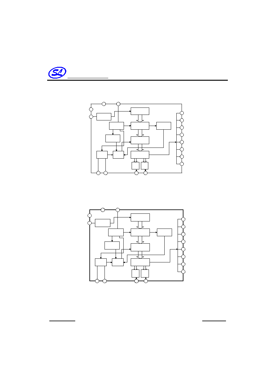
SC9149A Block Diagram
Input shift
register
Input Pulse
counter
Shift register
Data Check
Latch Circuit
Output Buffer
Code
Check
Error
Detection
F/F
F/F
Up Counter
OSC
11
12
13
14
15
2
1
16
10
9
8
7
6
5
4
3
VDD
OSC
CODE 2 CODE 3
SP1
SP2
SP3
CP1
CP2
HP1
HP2
HP3
HP4
HP5
GND
Rx IN
SC9149AL/9149AHN Block Diagram

Silan
Semiconductors
SC9149A/SC9150A
HANGZHOU SILAN MICROELECTRONICS CO.,LTD.
Rev: 1.2 2003.01.21
3
Input shift
register
Input Pulse
counter
Shift register
Data Check
Latch Circuit
Output Buffer
Code
Check
Error
Detection
F/F
F/F
Up Counter
OSC
21
22
23
2
1
24
10
9
8
7
6
5
4
3
VDD
OSC
CODE 2
CODE 1
SP1
SP2
SP3
SP4
SP10
HP1
HP2
HP3
HP4
HP5
GND
Rx IN
14
13
12
11
16
15
20
19
18
17
HP6
CP2
CP1
SP5
SP6
SP7
SP8
SP9
SC9150A Block Diagram
ABSOLUTE MAXIMUM RATINGS
(Ta=25
�C)
Characteristic Symbol Value
Unit
Supply Voltage
V
DD
0 ~ 6.0
V
Input / Output Voltage
V
IN
,V
OUT
Vss-0.3V ~ V
DD
+0.3V
V
Power Dissipation
P
D
200
mW
Operating Temperature
Tamb
-20 ~ +75
�C
Storage Temperature
Tstg
-55 ~ +125
�C
ELECTRICAL CHARACTERISTICS
(Tamb=25
�C,V
DD
=5.0V,Unless otherwise specified)
Parameter Symbol
Test
Conditions
Min
Typ
Max
Unit
Operating Supply Voltage
V
DD
Ta=25 ~ 75
�C 4.5
5.5
V
Operating Supply Current
I
DD
Output without Load
1.0
mA
Standard OSC Frequency
Sfosc
38
kHz
Oscillation Frequency
fosc
27
57
kHz
Variance Of Oscillation Frequency
By VDD
V
fosc
V
DD
=4.5~5.5V -5
5
%
Variance Of Oscillation Frequency
By Temperature
T
fosc
Ta=-30~+75
�C -5
5
%
"H" Level
I
OH
All output, V
OH
=4.0V
-1.0
mA
Output Current
"L" Level
I
OL
All Output, V
OL
=1V 1.0
mA
Input Current
"H" Level
I
IH
CODE Terminal, V
IH
=5.0V -1.0
1.0
�A
Pull-Up Resistor
Rup
CODE Terminal
10
20
40
k
Input Circuit Threshold Voltage
V
IN
Rx
Terminal
2.0 2.5 3.0 V
Hysteresis Width
V
HIS
Rx
Terminal
0.8 V

Silan
Semiconductors
SC9149A/SC9150A
HANGZHOU SILAN MICROELECTRONICS CO.,LTD.
Rev: 1.2 2003.01.21
4
PIN DESCRIPTION
Pin No.
SC9149A
SC9149AL
/9149AHN
SC9150A
Symbol Terminal
Function
/operation
Input/output
configuration
1 1 1
GND
GND
2 2 2
Rx
IN
Receiving
signal input
Instruction signal
with carrier
signal eliminated
is input.
3~7 3~7 --
HP1
~HP5
-- --
3~8
HP1
~HP6
Continuous
signal
output
As long as
receiving signal
is input, this
output is held at
"H" level
-- 9~8
9~10
CP1
~CP2
Cyclic
signal
output
When receiving
signal is input,
output is
reversed.
F/F
-- 12~10 --
SP1
~SP3
8~12 -- --
SP1
~SP5
-- --
11~20
SP1
~SP10
Single-shot
signal
output
When receiving
signal is input,
output is placed
at "H" level only
for a fixed
time.(about
107msec)
13,14 13~14 21~22
CODE
Code
input
Transmitter code
is compared with
a code set at this
terminal and if
they agree each
other, input is
accepted.
V
DD
Built-in pull-up resistor.
15 15 23
OSC
Timing
oscillation
A resistor and a
capacitor are
parallel
connected
between this
terminal and
GND.
V
DD
16 16 24
V
DD
Power
supply

Silan
Semiconductors
SC9149A/SC9150A
HANGZHOU SILAN MICROELECTRONICS CO.,LTD.
Rev: 1.2 2003.01.21
5
FUNCTIONAL DESCRIPTION
1. OSCILLATION CIRCUIT
Timing with transmitter signal and internal operating clock are all decided by this oscillator.
R
C
V
DD
osc
The oscillator has been so far constructed through a combination of a linear amplifier by means of CMOS inverter
in IC and 455kHz ceramic resonator ;however , when SC9149A/SC9150A series are used , a stable oscillator can
be constructed by parallel connecting C and R between the oscillator and GND by a single terminal oscillator .
Oscillation frequency is about 38KHz
�5 kHz at R=39k and C=1000pF. (Refer to SCILLATION Frequency
Characteristic below )
700
900
1100
1300
20
30
40
50
60
70
Capacitor (pF)
Oscillator
fr
equency (
k
H
z
)
V
DD
=5V
R=39k
20
30
40
50
60
70
Oscillator
fr
equency (
k
H
z
)
Resistor (k
26
34
42
50
58
V
DD
=5V
C=1000pF
Oscillator frequency vs. resistor and capacitor
2. RECEIVING SIGNAL INPUT CIRCUIT
Rx
Vcc
Det.
Amp.