PRINCIPAL RATINGS AND CHARACTERISTICS
PRINCIPAL RATINGS AND CHARACTERISTICS
PRINCIPAL RATINGS AND CHARACTERISTICS
PRINCIPAL RATINGS AND CHARACTERISTICS
PRINCIPAL RATINGS AND CHARACTERISTICS
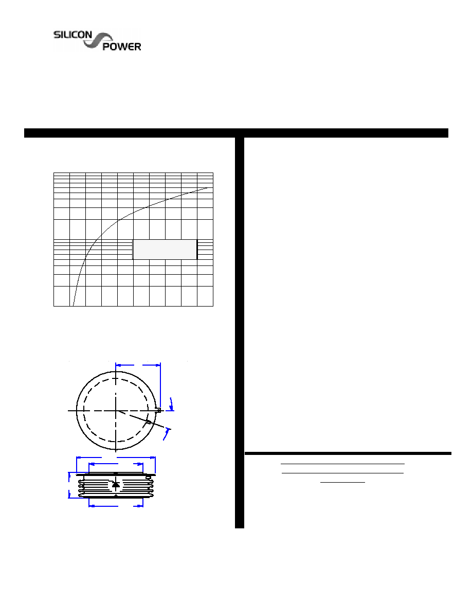
ON-STATE CHARACTERISTIC
ON-STATE CHARACTERISTIC
ON-STATE CHARACTERISTIC
ON-STATE CHARACTERISTIC
ON-STATE CHARACTERISTIC
MECHANICAL OUTLINE
MECHANICAL OUTLINE
MECHANICAL OUTLINE
MECHANICAL OUTLINE
MECHANICAL OUTLINE
100
1000
10000
0
1
2
3
4
5
6
7
8
9
10
On-state current , It (amperes)
On-state Voltage , Vt (volts)
On-state Voltage , Vt (volts)
Process Maximum
pulsed current
Tcase = 115 C
Repetitive peak off-
Repetitive peak off-
Repetitive peak off-
Repetitive peak off-
Repetitive peak off-
V
V
V
V
V
D R M
D R M
D R M
D R M
D R M
T
T
T
T
T
J
J
J
J
J
=0
=0
=0
=0
=0
up to
up to
up to
up to
up to
V
V
V
V
V
state & reverse volts
state & reverse volts
state & reverse volts
state & reverse volts
state & reverse volts
V
V
V
V
V
R R M
R R M
R R M
R R M
R R M
to 115
to 115
to 115
to 115
to 115
o
o
o
o
o
C
C
C
C
C
6000
6000
6000
6000
6000
Repetitive working
Repetitive working
Repetitive working
Repetitive working
Repetitive working
V
V
V
V
V
D W M
D W M
D W M
D W M
D W M
T
T
T
T
T
J
J
J
J
J
=0
=0
=0
=0
=0
0.8V
0.8V
0.8V
0.8V
0.8V
D R M
D R M
D R M
D R M
D R M
crest voltage
crest voltage
crest voltage
crest voltage
crest voltage
V
V
V
V
V
R W M
R W M
R W M
R W M
R W M
to 115
to 115
to 115
to 115
to 115
o
o
o
o
o
C
C
C
C
C
0.8V
0.8V
0.8V
0.8V
0.8V
R R M
R R M
R R M
R R M
R R M
off-state & reverse
off-state & reverse
off-state & reverse
off-state & reverse
off-state & reverse
I
I
I
I
I
D W M
D W M
D W M
D W M
D W M
T
T
T
T
T
J
J
J
J
J
=0
=0
=0
=0
=0
75
75
75
75
75
m a
m a
m a
m a
m a
leakage current
leakage current
leakage current
leakage current
leakage current
I
I
I
I
I
R W M
R W M
R W M
R W M
R W M
to 115
to 115
to 115
to 115
to 115
o
o
o
o
o
C
C
C
C
C
75
75
75
75
75
Average on-state
Average on-state
Average on-state
Average on-state
Average on-state
I
I
I
I
I
T(AV)
T(AV)
T(AV)
T(AV)
T(AV)
T
T
T
T
T
case
case
case
case
case
=
=
=
=
=
550
550
550
550
550
A
A
A
A
A
current
current
current
current
current
70
70
70
70
70
o
o
o
o
o
C
C
C
C
C
Peak half-cycle
Peak half-cycle
Peak half-cycle
Peak half-cycle
Peak half-cycle
I
I
I
I
I
T S M
T S M
T S M
T S M
T S M
60 Hz
60 Hz
60 Hz
60 Hz
60 Hz
6
6
6
6
6
kA
kA
kA
kA
kA
non-rep surge current
non-rep surge current
non-rep surge current
non-rep surge current
non-rep surge current
50 Hz
50 Hz
50 Hz
50 Hz
50 Hz
5.5
5.5
5.5
5.5
5.5
On-state voltage
On-state voltage
On-state voltage
On-state voltage
On-state voltage
V
V
V
V
V
T M
T M
T M
T M
T M
I
I
I
I
I
T
T
T
T
T
=500A
=500A
=500A
=500A
=500A
2.00
2.00
2.00
2.00
2.00
V
V
V
V
V
t
t
t
t
t
P
P
P
P
P
=8ms
=8ms
=8ms
=8ms
=8ms
T
T
T
T
T
J
J
J
J
J
=115
=115
=115
=115
=115
o
o
o
o
o
C
C
C
C
C
Critical rate of rise
Critical rate of rise
Critical rate of rise
Critical rate of rise
Critical rate of rise
di/dt
di/dt
di/dt
di/dt
di/dt
T
T
T
T
T
J
J
J
J
J
=115
=115
=115
=115
=115
o
o
o
o
o
C
C
C
C
C
50
50
50
50
50
A/us
A/us
A/us
A/us
A/us
of on-state current
of on-state current
of on-state current
of on-state current
of on-state current
rep
rep
rep
rep
rep
60 Hz
60 Hz
60 Hz
60 Hz
60 Hz
V
V
V
V
V
d
d
d
d
d
=.67V
=.67V
=.67V
=.67V
=.67V
D R M
D R M
D R M
D R M
D R M
allowable snubber discharge
allowable snubber discharge
allowable snubber discharge
allowable snubber discharge
allowable snubber discharge
50
50
50
50
50
A
A
A
A
A
Critical rate of rise
Critical rate of rise
Critical rate of rise
Critical rate of rise
Critical rate of rise
dv/dt
dv/dt
dv/dt
dv/dt
dv/dt
T
T
T
T
T
J
J
J
J
J
=115
=115
=115
=115
=115
o
o
o
o
o
C
C
C
C
C
1500
1500
1500
1500
1500
V/us
V/us
V/us
V/us
V/us
of off-state voltage
of off-state voltage
of off-state voltage
of off-state voltage
of off-state voltage
V
V
V
V
V
DCRIT
DCRIT
DCRIT
DCRIT
DCRIT
=60%V
=60%V
=60%V
=60%V
=60%V
D R M
D R M
D R M
D R M
D R M
Recovery current
Recovery current
Recovery current
Recovery current
Recovery current
I
I
I
I
I
R M
R M
R M
R M
R M
T
T
T
T
T
J
J
J
J
J
=115
=115
=115
=115
=115
o
o
o
o
o
C
C
C
C
C
A
A
A
A
A
2A/us
2A/us
2A/us
2A/us
2A/us
60
60
60
60
60
5A/us
5A/us
5A/us
5A/us
5A/us
100
100
100
100
100
minimum snap factor S = 0.3
minimum snap factor S = 0.3
minimum snap factor S = 0.3
minimum snap factor S = 0.3
minimum snap factor S = 0.3
Turn-on delay
Turn-on delay
Turn-on delay
Turn-on delay
Turn-on delay
t
t
t
t
t
d
d
d
d
d
Vd=.5V
Vd=.5V
Vd=.5V
Vd=.5V
Vd=.5V
D R M
D R M
D R M
D R M
D R M
5
5
5
5
5
us
us
us
us
us
Turn-off time
Turn-off time
Turn-off time
Turn-off time
Turn-off time
T
T
T
T
T
off
off
off
off
off
5A/us,-100V
5A/us,-100V
5A/us,-100V
5A/us,-100V
5A/us,-100V
600
600
600
600
600
us
us
us
us
us
20V/us to 2000V
20V/us to 2000V
20V/us to 2000V
20V/us to 2000V
20V/us to 2000V
Thermal resistance
Thermal resistance
Thermal resistance
Thermal resistance
Thermal resistance
R
R
R
R
R
thJC
thJC
thJC
thJC
thJC
.025
.025
.025
.025
.025
c/w
c/w
c/w
c/w
c/w
Externally applied
Externally applied
Externally applied
Externally applied
Externally applied
F
F
F
F
F
5500
5500
5500
5500
5500
lbs.
lbs.
lbs.
lbs.
lbs.
clamping force
clamping force
clamping force
clamping force
clamping force
24.5
24.5
24.5
24.5
24.5
kN
kN
kN
kN
kN
PG: 6.064 1/3/92
C716
C716
C716
C716
C716
53mm / 6kV THYRISTOR
53mm / 6kV THYRISTOR
53mm / 6kV THYRISTOR
53mm / 6kV THYRISTOR
53mm / 6kV THYRISTOR
REPETITIVE PEAK REVERSE
AND OFF-STATE BLOCKING
V O L T A G E
T
J
= 0 to 115
o
C
M O D E L
V
D R M
V
R R M
(volts)
(volts)
C716FP
6000
6000
C716ET
5900
5900
C716EN
5800
5800
C716ES
5700
5700
C716EM
5600
5600
C716EE
5500
5500
Type C716 thyristor is suitable for phase control applications such as HVDC valves, static
Type C716 thyristor is suitable for phase control applications such as HVDC valves, static
Type C716 thyristor is suitable for phase control applications such as HVDC valves, static
Type C716 thyristor is suitable for phase control applications such as HVDC valves, static
Type C716 thyristor is suitable for phase control applications such as HVDC valves, static
VAR compensators and synchronous motor drives.
VAR compensators and synchronous motor drives.
VAR compensators and synchronous motor drives.
VAR compensators and synchronous motor drives.
VAR compensators and synchronous motor drives.
The silicon junction is manufactured by the proven multi-diffusion process and is supplied in
The silicon junction is manufactured by the proven multi-diffusion process and is supplied in
The silicon junction is manufactured by the proven multi-diffusion process and is supplied in
The silicon junction is manufactured by the proven multi-diffusion process and is supplied in
The silicon junction is manufactured by the proven multi-diffusion process and is supplied in
an industry standard disc-type package, ready to mount to forced or naturally cooled heat
an industry standard disc-type package, ready to mount to forced or naturally cooled heat
an industry standard disc-type package, ready to mount to forced or naturally cooled heat
an industry standard disc-type package, ready to mount to forced or naturally cooled heat
an industry standard disc-type package, ready to mount to forced or naturally cooled heat
dissipators using commercially available mechanical clamping hardware.
dissipators using commercially available mechanical clamping hardware.
dissipators using commercially available mechanical clamping hardware.
dissipators using commercially available mechanical clamping hardware.
dissipators using commercially available mechanical clamping hardware.
175 GREAT VALLEY PKWY. MALVERN , PA 19355 USA
B �
B �
A �
2 0� �5 �
D
CL
CL
J
A
A
A
A
A
= 2.96 in (75.2 mm)
= 2.96 in (75.2 mm)
= 2.96 in (75.2 mm)
= 2.96 in (75.2 mm)
= 2.96 in (75.2 mm)
B
B
B
B
B
=1.90 in (48.3 mm)
=1.90 in (48.3 mm)
=1.90 in (48.3 mm)
=1.90 in (48.3 mm)
=1.90 in (48.3 mm)
D=1.07 in (27.2 mm)
D=1.07 in (27.2 mm)
D=1.07 in (27.2 mm)
D=1.07 in (27.2 mm)
D=1.07 in (27.2 mm)
0
250
500
750
1000
1250
1500
1750
2000
2250
2500
2750
3000
0
250
500
750
1000
1250
1500
1750
2000
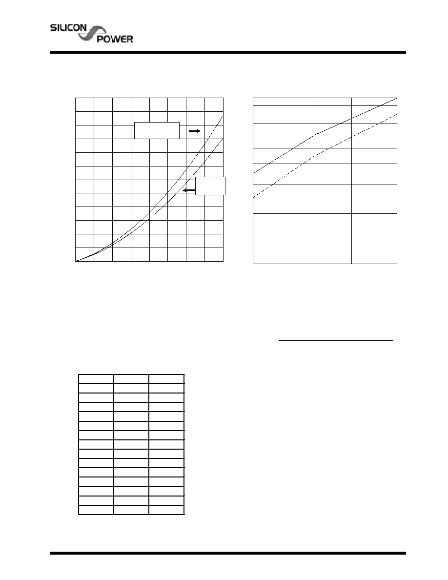
FULL CYCLE AVERAGE POWER LOSS
versus
PEAK CURRENT at 50/60 Hz
Average Power, Pavg (Watts)
Peak Current, It (Amperes)
Peak Current, It (Amperes)
c716los1(vt=2.0)
(plasma spreading and conduction loss)
overlap angle
= 20 degree
180 degree
sinewave
120 deg.sq. wave
10
100
1
MAXIMUM PEAK RECOVERY CURRENT
versus COMMUTATING di/dt
Peak Recovery Current, Irm, (A)
Circuit Commutating, di/dt, (A/us)
Circuit Commutating, di/dt, (A/us)
C716
25 degC
115 degC
3
5
GATE SUPPLY REQUIREMENTS
GATE SUPPLY REQUIREMENTS
GATE SUPPLY REQUIREMENTS
GATE SUPPLY REQUIREMENTS
GATE SUPPLY REQUIREMENTS
Open circuit voltage
30 V
Short circuit current
3 A
- rise time
0.5us
Pulse duration (min)
20 us
PG: 6.064 11/7/91
C716 / T116
Full Cycle Power Loss (watts)
50/60 Hz, T
J
=115
o
C
I
T
(peak)
Half-sine
3 Phase
(A)
180
o
120
o
100
45
48
200
97
106
300
157
173
400
224
250
500
299
336
600
381
431
700
470
535
800
566
647
900
670
769
1000
780
899
1200
1023
1186
1400
1293
1508
1600
1590
1864
1800
1914
2255
2000
2268
2680