September 2003
1
Document Control # ML0009 rev 0.1
STK15C68
8K x 8 AutoStoreTM nvSRAM
QuantumTrapTM CMOS
Nonvolatile Static RAM
FEATURES
∑ Nonvolatile Storage without Battery Problems
∑ Directly Replaces 8K x 8 Static RAM, Battery-
Backed RAM or EEPROM
∑ 25ns, 35ns and 45ns Access Times
∑ STORE to Nonvolatile Elements Initiated by
Software or AutoStoreTM on Power Down
∑ RECALL to SRAM Initiated by Software or
Power Restore
∑ 10mA Typical I
CC
at 200ns Cycle Time
∑ Unlimited READ, WRITE and RECALL Cycles
∑ 1,000,000 STORE Cycles to Nonvolatile Ele-
ments
∑ 100-Year Data Retention over Full Industrial
Temperature Range
∑ No Data Loss from Undershoot
∑ Commercial and Industrial Temperatures
∑ 28-Pin 600 or 300 mil PDIP and 350 mil SOIC
Packages
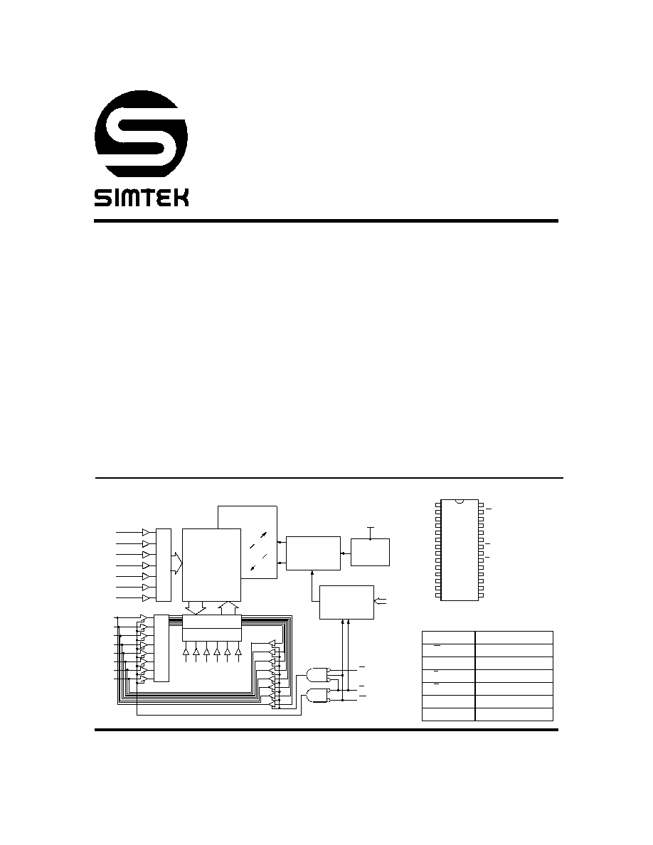
DESCRIPTION
The STK15C68 is a fast
SRAM
with a nonvolatile ele-
ment incorporated in each static memory cell. The
SRAM
can be read and written an unlimited number of
times, while independent nonvolatile data resides in
Nonvolatile Elements. Data transfers from the
SRAM
to
the Nonvolatile Elements (the
STORE
operation) can
take place automatically on power down using charge
stored in system capacitance. Transfers from the Non-
volatile Elements to the
SRAM
(the
RECALL
operation)
take place automatically on restoration of power. Initia-
tion of
STORE
and
RECALL
cycles can also be con-
trolled by entering control sequences on the
SRAM
inputs. The STK15C68 is pin-compatible with 8k x 8
SRAM
s and battery-backed
SRAM
s, allowing direct
substitution while enhancing performance. A similar
device (STK16C68) with an internally integrated
capacitor is available for systems with very fast slew
rates. The STK12C68, which uses an external capaci-
tor, is an alternative for these applications.
BLOCK DIAGRAM
COLUMN I/O
COLUMN DEC
STATIC RAM
ARRAY
128 x 512
R
O
W
DE
CO
DE
R
IN
PUT BUFFE
RS
QUANTUM TRAP
128 x 512
STORE/
RECALL
CONTROL
STORE
RECALL
POWER
CONTROL
A
5
A
6
A
9
A
11
A
12
DQ
0
DQ
1
DQ
2
DQ
3
DQ
4
DQ
5
DQ
6
DQ
7
SOFTWARE
DETECT
V
CC
A
0
-
A
12
G
E
W
A
8
A
7
A
10
A
3
A
2
A
0
A
1
A
4
PIN NAMES
A
0
- A
12
Address Inputs
W
Write Enable
DQ
0
- DQ
7
Data In/Out
E
Chip Enable
G
Output Enable
V
CC
Power (+ 5V)
V
SS
Ground
PIN CONFIGURATIONS
NC
A
12
A
7
A
6
A
5
A
4
A
3
A
2
A
1
A
0
DQ
0
DQ
1
DQ
2
V
SS
V
CC
NC
A
8
A
9
A
11
G
W
1
2
3
4
5
6
7
8
9
10
11
12
13
14
28
27
26
25
24
23
22
21
20
19
18
17
16
15
A
10
E
DQ
7
DQ
6
DQ
5
DQ
4
DQ
3
28 - 300 PDIP
28 - 600 PDIP
28 - 350 SOIC
STK15C68
September 2003
2
Document Control # ML0009 rev 0.1
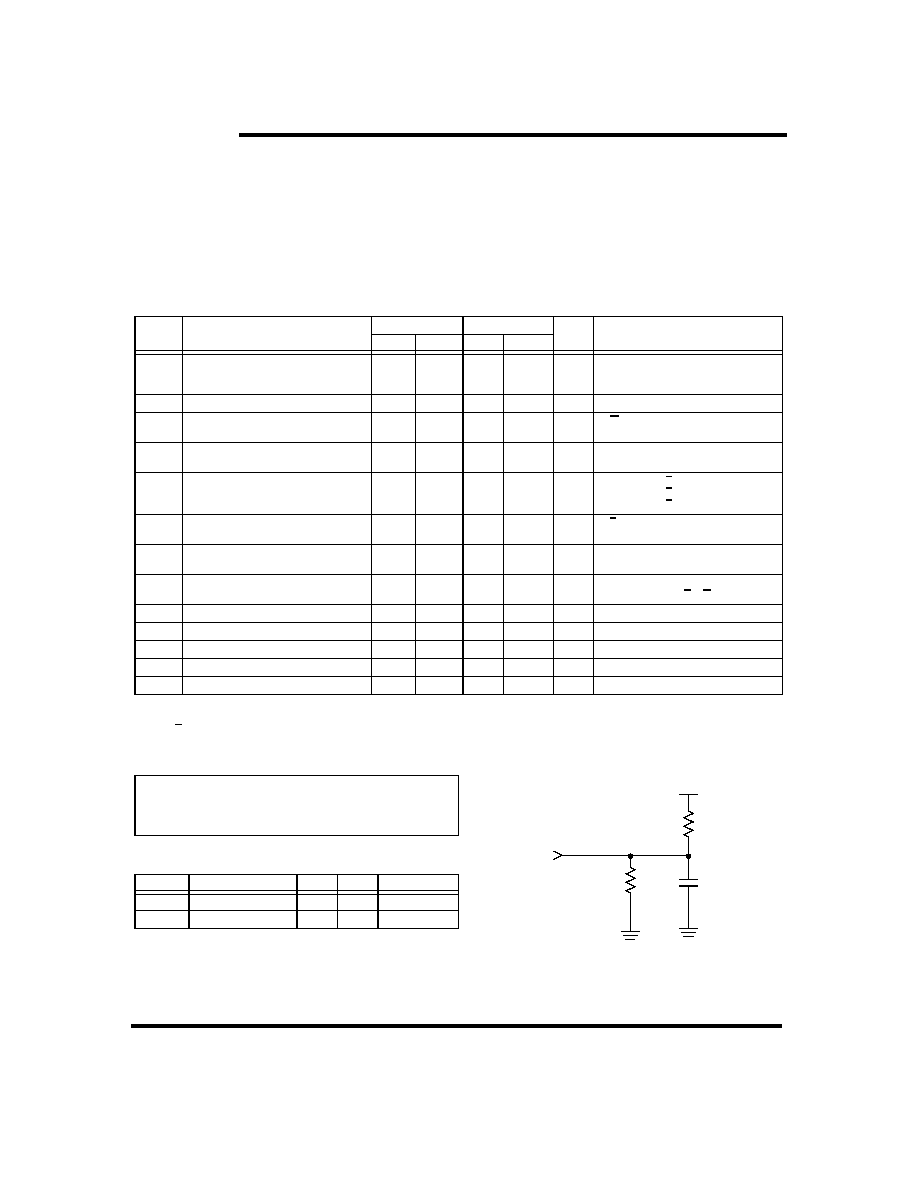
ABSOLUTE MAXIMUM RATINGS
a
Voltage on Input Relative to Ground . . . . . . . . . . . . . .≠0.5V to 7.0V
Voltage on Input Relative to V
SS
. . . . . . . . . . ≠0.6V to (V
CC
+ 0.5V)
Voltage on DQ
0-7
. . . . . . . . . . . . . . . . . . . . . . ≠0.5V to (V
CC
+ 0.5V)
Temperature under Bias . . . . . . . . . . . . . . . . . . . . . ≠55
∞
C to 125
∞
C
Storage Temperature . . . . . . . . . . . . . . . . . . . . . . . ≠65
∞
C to 150
∞
C
Power Dissipation . . . . . . . . . . . . . . . . . . . . . . . . . . . . . . . . . . . . 1W
DC Output Current (1 output at a time, 1s duration) . . . . . . . . 15mA
DC CHARACTERISTICS
(V
CC
= 5.0V
±
10%)
Note b: I
CC1
and I
CC3
are dependent on output loading and cycle rate. The specified values are obtained with outputs unloaded.
Note c: I
CC2
and I
CC4
are the average currents required for the duration of the respective
STORE
cycles (t
STORE
) .
Note d: E
V
IH
will not produce standby current levels until any nonvolatile cycle in progress has timed out.
AC TEST CONDITIONS
CAPACITANCE
e
(T
A
= 25
∞
C, f = 1.0MHz)
Note e: These parameters are guaranteed but not tested.
SYMBOL
PARAMETER
COMMERCIAL
INDUSTRIAL
UNITS
NOTES
MIN
MAX
MIN
MAX
I
CC1
b
Average V
CC
Current
85
75
65
90
75
65
mA
mA
mA
t
AVAV
= 25ns
t
AVAV
= 35ns
t
AVAV
= 45ns
I
CC2
c
Average V
CC
Current during STORE
3
3
mA
All Inputs Don't Care, V
CC
= max
I
CC3
b
Average V
CC
Current at t
AVAV
= 200ns
5V, 25∞C, Typical
10
10
mA
W
(V
CC
≠ 0.2V)
All Others Cycling, CMOS Levels
I
CC4
c
Average V
CC
Current during
AutoStoreTM Cycle
2
2
mA
All Inputs Don't Care
I
SB1
d
Average
V
CC
Current
(Standby, Cycling TTL Input Levels)
27
23
20
28
24
21
mA
mA
mA
t
AVAV
= 25ns, E
V
IH
t
AVAV
= 35ns, E
V
IH
t
AVAV
= 45ns, E
V
IH
I
SB2
d
V
CC
Standby Current
(Standby, Stable CMOS Input Levels)
1.5
1.5
mA
E
(V
CC
≠ 0.2V)
All Others V
IN
0.2V or
(V
CC
≠ 0.2V)
I
ILK
Input Leakage Current
±
1
±
1
µ
A
V
CC
= max
V
IN
= V
SS
to V
CC
I
OLK
Off-State Output Leakage Current
±
5
±
5
µ
A
V
CC
= max
V
IN
= V
SS
to V
CC
, E or G
V
IH
V
IH
Input Logic "1" Voltage
2.2
V
CC
+ .5
2.2
V
CC
+ .5
V
All Inputs
V
IL
Input Logic "0" Voltage
V
SS
≠ .5
0.8
V
SS
≠ .5
0.8
V
All Inputs
V
OH
Output Logic "1" Voltage
2.4
2.4
V
I
OUT
= ≠ 4mA
V
OL
Output Logic "0" Voltage
0.4
0.4
V
I
OUT
= 8mA
T
A
Operating Temperature
0
70
≠40
85
∞
C
Input Pulse Levels . . . . . . . . . . . . . . . . . . . . . . . . . . . . . . . 0V to 3V
Input Rise and Fall Times
. . . . . . . . . . . . . . . . . . . . . . . . . . . . . . .
5ns
Input and Output Timing Reference Levels . . . . . . . . . . . . . . . 1.5V
Output Load . . . . . . . . . . . . . . . . . . . . . . . . . . . . . . . . . See Figure 1
SYMBOL
PARAMETER
MAX
UNITS
CONDITIONS
C
IN
Input capacitance
8
pF
V = 0 to 3V
C
OUT
Output Capacitance
7
pF
V = 0 to 3V
Figure 1: AC Output Loading
480 Ohms
30 pF
255 Ohms
5.0V
INCLUDING
OUTPUT
SCOPE AND
FIXTURE
Note a: Stresses greater than those listed under "Absolute Maximum
Ratings" may cause permanent damage to the device. This is a
stress rating only, and functional operation of the device at condi-
tions above those indicated in the operational sections of this
specification is not implied. Exposure to absolute maximum rat-
ing conditions for extended periods may affect reliability.

STK15C68
September 2003
3
Document Control # ML0009 rev 0.1
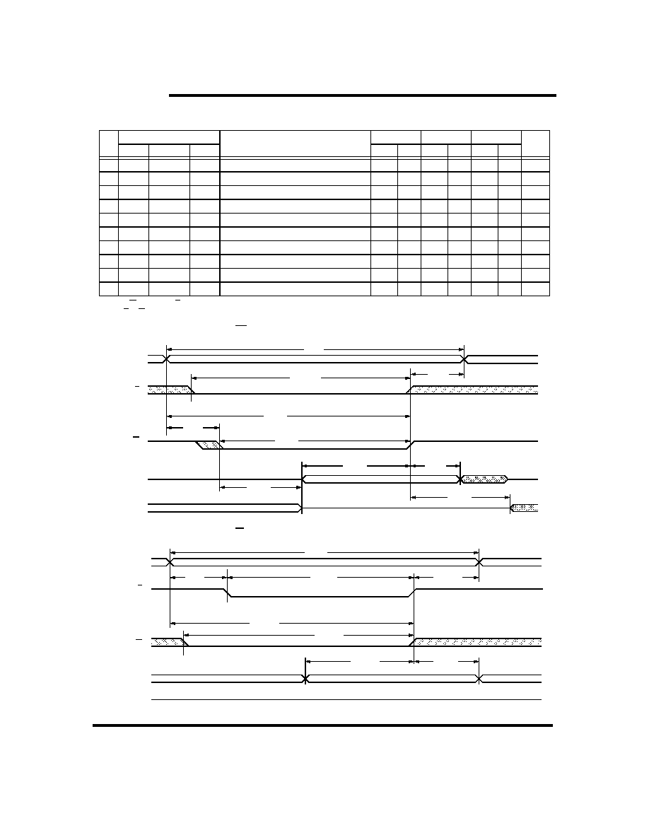
SRAM READ CYCLES #1 & #2
(V
CC
= 5.0V
±
10%)
Note f:
W must be high during SRAM READ cycles and low during SRAM WRITE cycles.
Note g: I/O state assumes E, G < V
IL
and W > V
IH
; device is continuously selected.
Note h: Measured + 200mV from steady state output voltage.
SRAM READ CYCLE #1: Address Controlled
f, g
SRAM READ CYCLE #2: E Controlled
f
NO.
SYMBOLS
PARAMETER
STK15C68-25
STK15C68-35
STK15C68-45
UNITS
#1, #2
Alt.
MIN
MAX
MIN
MAX
MIN
MAX
1
t
ELQV
t
ACS
Chip Enable Access Time
25
35
45
ns
2
t
AVAV
f
t
RC
Read Cycle Time
25
35
45
ns
3
t
AVQV
g
t
AA
Address Access Time
25
35
45
ns
4
t
GLQV
t
OE
Output Enable to Data Valid
10
15
20
ns
5
t
AXQX
g
t
OH
Output Hold after Address Change
5
5
5
ns
6
t
ELQX
t
LZ
Chip Enable to Output Active
5
5
5
ns
7
t
EHQZ
h
t
HZ
Chip Disable to Output Inactive
10
13
15
ns
8
t
GLQX
t
OLZ
Output Enable to Output Active
0
0
0
ns
9
t
GHQZ
h
t
OHZ
Output Disable to Output Inactive
10
13
15
ns
10
t
ELICCH
e
t
PA
Chip Enable to Power Active
0
0
0
ns
11
t
EHICCL
d, e
t
PS
Chip Disable to Power Standby
25
35
45
ns
DATA VALID
5
t
AXQX
3
t
AVQV
DQ (DATA OUT)
ADDRESS
2
t
AVAV
6
t
ELQX
STANDBY
DATA VALID
8
t
GLQX
4
t
GLQV
DQ (DATA OUT)
E
ADDRESS
2
t
AVAV
G
I
CC
ACTIVE
1
t
ELQV
10
t
ELICCH
11
t
EHICCL
7
t
EHQZ
9
t
GHQZ
STK15C68
September 2003
4
Document Control # ML0009 rev 0.1
SRAM WRITE CYCLES #1 & #2
(V
CC
= 5.0V
±
10%)
Note i:
If W is low when E goes low, the outputs remain in the high-impedance state.
Note j:
E or W must be
V
IH
during address transitions.
SRAM WRITE CYCLE #1: W Controlled
j
SRAM WRITE CYCLE #2: E Controlled
j
NO.
SYMBOLS
PARAMETER
STK15C68-25
STK15C68-35
STK15C68-45
UNITS
#1
#2
Alt.
MIN
MAX
MIN
MAX
MIN
MAX
12
t
AVAV
t
AVAV
t
WC
Write Cycle Time
25
35
45
ns
13
t
WLWH
t
WLEH
t
WP
Write Pulse Width
20
25
30
ns
14
t
ELWH
t
ELEH
t
CW
Chip Enable to End of Write
20
25
30
ns
15
t
DVWH
t
DVEH
t
DW
Data Set-up to End of Write
10
12
15
ns
16
t
WHDX
t
EHDX
t
DH
Data Hold after End of Write
0
0
0
ns
17
t
AVWH
t
AVEH
t
AW
Address Set-up to End of Write
20
25
30
ns
18
t
AVWL
t
AVEL
t
AS
Address Set-up to Start of Write
0
0
0
ns
19
t
WHAX
t
EHAX
t
WR
Address Hold after End of Write
0
0
0
ns
20
t
WLQZ
h, i
t
WZ
Write Enable to Output Disable
10
13
15
ns
21
t
WHQX
t
OW
Output Active after End of Write
5
5
5
ns
PREVIOUS DATA
DATA OUT
E
ADDRESS
12
t
AVAV
W
16
t
WHDX
DATA IN
19
t
WHAX
13
t
WLWH
18
t
AVWL
17
t
AVWH
DATA VALID
20
t
WLQZ
15
t
DVWH
HIGH IMPEDANCE
21
t
WHQX
14
t
ELWH
W
DATA OUT
E
ADDRESS
12
t
AVAV
W
DATA IN
13
t
WLEH
1 7
t
AVEH
DATA VALID
HIGH IMPEDANCE
14
t
ELEH
18
t
AVEL
19
t
EHAX
15
t
DVEH
16
t
EHDX
STK15C68
September 2003
5
Document Control # ML0009 rev 0.1
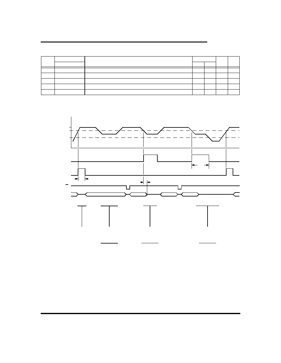
AutoStoreTM/POWER-UP RECALL
(V
CC
= 5.0V
±
10%)
Note k: t
RESTORE
starts from the time V
CC
rises above V
SWITCH
.
AutoStoreTM/POWER-UP RECALL
NO.
SYMBOLS
PARAMETER
STK15C68
UNITS NOTES
Standard
MIN
MAX
22
t
RESTORE
Power-up RECALL Duration
550
µ
s
k
23
t
STORE
STORE Cycle Duration
10
ms
g
24
t
DELAY
Time Allowed to Complete SRAM Cycle
1
µ
s
g
25
V
SWITCH
Low Voltage Trigger Level
4.0
4.5
V
26
V
RESET
Low Voltage Reset Level
3.6
V
e
V
CC
V
SWITCH
V
RESET
POWER-UP RECALL
W
DQ (DATA OUT)
AutoStoreTM
5V
22
t
RESTORE
24
t
DELAY
23
t
STORE
25
26
BROWN OUT
AutoStoreTM
NO RECALL
(V
CC
DID NOT GO
BELOW V
RESET
)
BROWN OUT
AutoStoreTM
RECALL WHEN
V
CC
RETURNS
ABOVE V
SWITCH
POWER-UP
RECALL
BROWN OUT
NO STORE DUE TO
NO SRAM WRITES
NO RECALL
(V
CC
DID NOT GO
BELOW V
RESET
)