
September 2003
1
Document Control # ML0005 rev 0.1
STK25C48
2K x 8 AutoStoreTM nvSRAM
QuantumTrapTM CMOS
Nonvolatile Static RAM
FEATURES
∑ Nonvolatile Storage without Battery Problems
∑ Directly Replaces 2K x 8 Static RAM, Battery-
Backed RAM or EEPROMs
∑ 25ns, 35ns and 45ns Access Times
∑ STORE to Nonvolatile Elements Initiated by
AutoStoreTM on Power Down
∑ RECALL to SRAM Initiated by Power Restore
∑ 10mA Typical I
CC
at 200ns Cycle Time
∑ Unlimited READ, WRITE and RECALL Cycles
∑ 1,000,000 STORE Cycles to Nonvolatile Ele-
ments
∑ 100-Year Data Retention over Full Industrial
Temperature Range
∑ Commercial and Industrial Temperatures
∑ 24-Pin 600 PDIP Package
DESCRIPTION
The STK25C48 is a fast
SRAM
with a nonvolatile element
incorporated in each static memory cell. The
SRAM
can
be read and written an unlimited number of times, while
independent nonvolatile data resides in the
Nonvolatile
Elements
. Data transfers from the
SRAM
to the
Nonvola-
tile Elements
(the
STORE
operation) can take place auto-
matically on power down using charge stored in system
capacitance. Transfers from the
Nonvolatile Elements
to
the
SRAM
(the
RECALL
operation) take place automati-
cally on restoration of power. The nv
SRAM
can be used in
place of existing 2K x 8
SRAM
s and also matches the
pinout of 2K x 8 battery-backed
SRAM
s,
EPROM
s and
EEPROM
s, allowing direct substitution while enhancing
performance. No support circuitry is required for micro-
processor interfacing.
BLOCK DIAGRAM
COLUMN I/O
COLUMN DEC
STATIC RAM
ARRAY
32 x 512
ROW DE
CODE
R
INPU
T B
U
FFERS
QUANTUM TRAP
32 x 512
STORE/
RECALL
CONTROL
STORE
RECALL
POWER
CONTROL
A
5
A
6
A
9
DQ
0
DQ
1
DQ
2
DQ
3
DQ
4
DQ
5
DQ
6
DQ
7
V
CC
G
E
W
A
8
A
7
A
10
A
3
A
2
A
0
A
1
A
4
PIN CONFIGURATIONS
V
CC
A
9
W
G
A
10
E
A
8
1
2
3
4
5
6
7
8
9
10
11
12
24
23
22
21
20
19
18
17
16
15
14
13
DQ
7
DQ
6
DQ
5
DQ
4
DQ
3
A
7
A
5
A
4
A
3
A
2
A
1
A
0
DQ
0
DQ
1
DQ
2
V
SS
A
6
24 - 600 PDIP
PIN NAMES
A
0
- A
10
Address Inputs
W
Write Enable
DQ
0
- DQ
7
Data In/Out
E
Chip Enable
G
Output Enable
V
CC
Power (+ 5V)
V
SS
Ground

STK25C48
September 2003
2
Document Control # ML0005 rev 0.1
ABSOLUTE MAXIMUM RATINGS
a
Voltage on Input Relative to Ground . . . . . . . . . . . . . .≠0.5V to 7.0V
Voltage on Input Relative to V
SS
. . . . . . . . . . ≠0.6V to (V
CC
+ 0.5V)
Voltage on DQ
0-7
. . . . . . . . . . . . . . . . . . . . . . ≠0.5V to (V
CC
+ 0.5V)
Temperature under Bias . . . . . . . . . . . . . . . . . . . . . ≠55
∞
C to 125
∞
C
Storage Temperature . . . . . . . . . . . . . . . . . . . . . . . ≠65
∞
C to 150
∞
C
Power Dissipation . . . . . . . . . . . . . . . . . . . . . . . . . . . . . . . . . . . . 1W
DC Output Current (1 output at a time, 1s duration) . . . . . . . . 15mA
DC CHARACTERISTICS
(V
CC
= 5.0V
±
10%)
Note b: I
CC1
and I
CC3
are dependent on output loading and cycle rate. The specified values are obtained with outputs unloaded.
Note c: I
CC2
and I
CC4
are the average currents required for the duration of the respective
STORE
cycles (t
STORE
) .
Note d: E
V
IH
will not produce standby current levels until any nonvolatile cycle in progress has timed out.
AC TEST CONDITIONS
CAPACITANCE
e
(T
A
= 25
∞
C, f = 1.0MHz)
Note e: These parameters are guaranteed but not tested.
SYMBOL
PARAMETER
COMMERCIAL
INDUSTRIAL
UNITS
NOTES
MIN
MAX
MIN
MAX
I
CC1
b
Average V
CC
Current
85
75
65
90
75
65
mA
mA
mA
t
AVAV
= 25ns
t
AVAV
= 35ns
t
AVAV
= 45ns
I
CC2
c
Average V
CC
Current during STORE
3
3
mA
All Inputs Don't Care, V
CC
= max
I
CC3
b
Average V
CC
Current at t
AVAV
= 200ns
5V, 25∞C, Typical
10
10
mA
W
(V
CC
≠ 0.2V)
All Others Cycling, CMOS Levels
I
CC4
c
Average V
CAP
Current during
AutoStoreTM Cycle
2
2
mA
All Inputs Don't Care
I
SB1
d
Average
V
CC
Current
(Standby, Cycling TTL Input Levels)
25
21
18
26
22
19
mA
mA
mA
t
AVAV
= 25ns, E
V
IH
t
AVAV
= 35ns, E
V
IH
t
AVAV
= 45ns, E
V
IH
I
SB2
d
V
CC
Standby Current
(Standby, Stable CMOS Input Levels)
1.5
1.5
mA
E
(V
CC
≠ 0.2V)
All Others V
IN
0.2V or
(V
CC
≠ 0.2V)
I
ILK
Input Leakage Current
±
1
±
1
µ
A
V
CC
= max
V
IN
= V
SS
to V
CC
I
OLK
Off-State Output Leakage Current
±
5
±
5
µ
A
V
CC
= max
V
IN
= V
SS
to V
CC
, E or G
V
IH
V
IH
Input Logic "1" Voltage
2.2
V
CC
+ .5
2.2
V
CC
+ .5
V
All Inputs
V
IL
Input Logic "0" Voltage
V
SS
≠ .5
0.8
V
SS
≠ .5
0.8
V
All Inputs
V
OH
Output Logic "1" Voltage
2.4
2.4
V
I
OUT
= ≠ 4mA
V
OL
Output Logic "0" Voltage
0.4
0.4
V
I
OUT
= 8mA
T
A
Operating Temperature
0
70
≠40
85
∞
C
Input Pulse Levels . . . . . . . . . . . . . . . . . . . . . . . . . . . . . . . 0V to 3V
Input Rise and Fall Times
. . . . . . . . . . . . . . . . . . . . . . . . . . . . . . .
5ns
Input and Output Timing Reference Levels . . . . . . . . . . . . . . . 1.5V
Output Load . . . . . . . . . . . . . . . . . . . . . . . . . . . . . . . . . See Figure 1
SYMBOL
PARAMETER
MAX
UNITS
CONDITIONS
C
IN
Input Capacitance
8
pF
V = 0 to 3V
C
OUT
Output Capacitance
7
pF
V = 0 to 3V
Figure 1: AC Output Loading
480 Ohms
30 pF
255 Ohms
5.0V
INCLUDING
OUTPUT
SCOPE AND
FIXTURE
Note a: Stresses greater than those listed under "Absolute Maximum
Ratings" may cause permanent damage to the device. This is a
stress rating only, and functional operation of the device at condi-
tions above those indicated in the operational sections of this
specification is not implied. Exposure to absolute maximum rat-
ing conditions for extended periods may affect reliability.
STK25C48
September 2003
3
Document Control # ML0005 rev 0.1
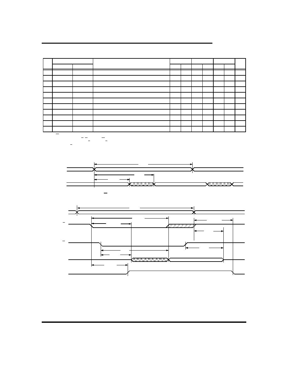
SRAM READ CYCLES #1 & #2
(V
CC
= 5.0V
±
10%)
Note f:
W must be high during SRAM READ cycles and low during SRAM WRITE cycles.
Note g: I/O state assumes E, G < V
IL
and W > V
IH
; device is continuously selected.
Note h: Measured + 200mV from steady state output voltage.
SRAM READ CYCLE #1: Address Controlled
f, g
SRAM READ CYCLE #2: E Controlled
f
NO.
SYMBOLS
PARAMETER
STK25C48-25
STK25C48-35
STK25C48-45
UNITS
#1, #2
Alt.
MIN
MAX
MIN
MAX
MIN
MAX
1
t
ELQV
t
ACS
Chip Enable Access Time
25
35
45
ns
2
t
AVAV
f
t
RC
Read Cycle Time
25
35
45
ns
3
t
AVQV
g
t
AA
Address Access Time
25
35
45
ns
4
t
GLQV
t
OE
Output Enable to Data Valid
10
15
20
ns
5
t
AXQX
g
t
OH
Output Hold after Address Change
5
5
5
ns
6
t
ELQX
t
LZ
Chip Enable to Output Active
5
5
5
ns
7
t
EHQZ
h
t
HZ
Chip Disable to Output Inactive
10
13
15
ns
8
t
GLQX
t
OLZ
Output Enable to Output Active
0
0
0
ns
9
t
GHQZ
h
t
OHZ
Output Disable to Output Inactive
10
13
15
ns
10
t
ELICCH
e
t
PA
Chip Enable to Power Active
0
0
0
ns
11
t
EHICCL
d, e
t
PS
Chip Disable to Power Standby
25
35
45
ns
DATA VALID
5
t
AXQX
3
t
AVQV
DQ (DATA OUT)
ADDRESS
2
t
AVAV
6
t
ELQX
STANDBY
DATA VALID
8
t
GLQX
4
t
GLQV
DQ (DATA OUT)
E
ADDRESS
2
t
AVAV
G
I
CC
ACTIVE
1
t
ELQV
10
t
ELICCH
11
t
EHICCL
7
t
EHQZ
9
t
GHQZ

STK25C48
September 2003
4
Document Control # ML0005 rev 0.1
SRAM WRITE CYCLES #1 & #2
(V
CC
= 5.0V
±
10%)
Note i:
If W is low when E goes low, the outputs remain in the high-impedance state.
Note j:
E or W must be
V
IH
during address transitions.
SRAM WRITE CYCLE #1: W Controlled
j
SRAM WRITE CYCLE #2: E Controlled
j
NO.
SYMBOLS
PARAMETER
STK25C48-25
STK25C48-35
STK25C48-45
UNITS
#1
#2
Alt.
MIN
MAX
MIN
MAX
MIN
MAX
12
t
AVAV
t
AVAV
t
WC
Write Cycle Time
25
35
45
ns
13
t
WLWH
t
WLEH
t
WP
Write Pulse Width
20
25
30
ns
14
t
ELWH
t
ELEH
t
CW
Chip Enable to End of Write
20
25
30
ns
15
t
DVWH
t
DVEH
t
DW
Data Set-up to End of Write
10
12
15
ns
16
t
WHDX
t
EHDX
t
DH
Data Hold after End of Write
0
0
0
ns
17
t
AVWH
t
AVEH
t
AW
Address Set-up to End of Write
20
25
30
ns
18
t
AVWL
t
AVEL
t
AS
Address Set-up to Start of Write
0
0
0
ns
19
t
WHAX
t
EHAX
t
WR
Address Hold after End of Write
0
0
0
ns
20
t
WLQZ
h, i
t
WZ
Write Enable to Output Disable
10
13
15
ns
21
t
WHQX
t
OW
Output Active after End of Write
5
5
5
ns
PREVIOUS DATA
DATA OUT
E
ADDRESS
12
t
AVAV
W
16
t
WHDX
DATA IN
19
t
WHAX
13
t
WLWH
18
t
AVWL
17
t
AVWH
DATA VALID
20
t
WLQZ
15
t
DVWH
HIGH IMPEDANCE
21
t
WHQX
14
t
ELWH
DATA OUT
E
ADDRESS
12
t
AVAV
W
DATA IN
13
t
WLEH
1 7
t
AVEH
DATA VALID
HIGH IMPEDANCE
14
t
ELEH
18
t
AVEL
19
t
EHAX
15
t
DVEH
16
t
EHDX

STK25C48
September 2003
5
Document Control # ML0005 rev 0.1
AutoStoreTM/POWER-UP RECALL
(V
CC
= 5.0V ± 10%)
Note k: t
RESTORE
starts from the time V
CC
rises above V
SWITCH
.
AutoStoreTM/POWER-UP RECALL
NO.
SYMBOLS
PARAMETER
STK25C48
UNITS NOTES
Standard
MIN
MAX
22
t
RESTORE
Power-up RECALL Duration
550
µ
s
k
23
t
STORE
STORE Cycle Duration
10
ms
g
24
t
DELAY
Time Allowed to Complete SRAM Cycle
1
µ
s
g
25
V
SWITCH
Low Voltage Trigger Level
4.0
4.5
V
26
V
RESET
Low Voltage Reset Level
3.6
V
e
V
CC
V
SWITCH
V
RESET
POWER-UP RECALL
W
DQ (DATA OUT)
AutoStoreTM
5V
22
t
RESTORE
24
t
DELAY
23
t
STORE
25
26
BROWN OUT
AutoStoreTM
NO RECALL
(V
CC
DID NOT GO
BELOW V
RESET
)
BROWN OUT
AutoStoreTM
RECALL WHEN
V
CC
RETURNS
ABOVE V
SWITCH
POWER-UP
RECALL
BROWN OUT
NO STORE DUE TO
NO SRAM WRITES
NO RECALL
(V
CC
DID NOT GO
BELOW V
RESET
)