
Now Available in Lead Free Packaging
Rev. 8/10/01
LP2950/51 100mA Low Dropout Voltage Regulators
©Copyright 2001 Sipex Corporation
1
INPUT
OUTPUT
UNREGULATED DC
SHUTDOWN
GROUND
ERROR
______
SENSE
5V @ 100mA
MAX
TO CMOS OR
TTL
REFERENCE
ERROR DETECTION
COMPARATOR
ERROR
AMPLIFIER
1.23V
FROM
CMOS OR
TTL
+
+
+
+
+
+
60 mV
3
7
8
1
2
6
5
4
60k
330k
180k
.
.
1
µ
F
_
_
FEEDBACK
5V TAP
LP2950/LP2951
100mA Low Dropout Voltage Regulators
FEATURES
APPLICATIONS
∑
5.0V and 3.3V Versions at 100mA Output
∑
Battery Powered Systems
∑
Very Low Quiescent Current
∑
Cordless Telephones
∑
Low Dropout Voltage: 380mV at 100mA
∑
Radio Control Systems
∑
Extremely Tight Load and Line Regulation
∑
Portable/Palm Top/Notebook Computers
∑
Very Low Temperature Coefficient
∑
Portable Consumer Equipment
∑
Current & Thermal Limiting
∑
Portable Instrumentation
∑
Need Only 1
µ
F for Stability
∑
Avionics
∑
Offered in TO-92 (LP2950) & SOIC (LP2951)
∑
SMPS Post-Regulator
∑
Direct Replacement For LP2950/LP2951
∑
Voltage Reference
∑
Automotive Electronics
LP2951 versions only
∑
Error Flag Warns of Output Dropout
∑
Logic-Controlled Electronic Shutdown
∑
Output Programmable From 1.24 to 29V
PRODUCT DESCRIPTION
The LP2950 and LP2951 are low power voltage regulators. These devices are an excellent choice for use in battery-powered
applications such as cordless telephones, radio control systems, and portable computers. The LP2950 and LP2951 feature low
quiescent current and low dropout voltage (typ. 50mV at light load and 380 mV at 100mA). This includes a tight initial tolerance
(0.5% typ.), extremely good load and line regulation (0.05% typ.), and very low output temperature coefficient (20 ppm/°C typ.),
making the LP2950/LP2951 useful as a low-power voltage reference.
The error flag output feature is used as a power-on reset for warning of a low output voltage, due to a falling input voltage. The logic-
compatible shutdown feature enables the regulator to be switched ON and OFF. The LP2950 is offered in a 3-pin TO-92 package
compatible with other 5V, 3.3V regulators. The LP2951 is available in an 8-lead SOIC package.
Block diagram of LP2951

Rev. 8/10/01
LP2950/51 100mA Low Dropout Voltage Regulators
©Copyright 2001 Sipex Corporation
2
LP2950/51
ABSOLUTE MAXIMUM RATINGS
Power Dissipation.....................................Internally Limited
Feedback Input Voltage................................................ -1.5V to +30V
Lead Temp. (Soldering, 5 Seconds)............................260°C
Shutdown Input Voltage............................................... -0.3V to +30V
Storage Temperature Range ......................... -65° to +150°C
Error Comparator Output ............................................. -0.3V to +30V
Operating Junction Temperature Range -40C to +125C
ESD Rating .........................................................................2kV Min
Input Supply Voltage..................................... -0.3V to +30V
ELECTRICAL CHARACTERISTICS V
IN
=6V, I
O
=100µA, C
OUT
=1µF (Note 2) T
A
=25C,
unless otherwise noted
.
PARAMETER
CONDITIONS
LP2950AC
LP2951AC
Min. Typ. Max.
LP2950C
LP2951C
Min. Typ. Max.
UNITS
3.3 V Versions
Output Voltage
TJ = 25°C
-25°C
TJ
85°C
Full Operating Temperature
3.284
3.267
3.260
3.3
3.3
3.3
3.317
3.333
3.340
3.267
3.251
3.234
3.3
3.3
3.3
3.333
3.350
3.366
V
Output Voltage
100
µ
A
I
L
100 mA
TJ
T
JMAX
3.254
3.3
3.346
3.221
3.3
3.379
V
5 V Versions
Output Voltage
T
J
= 25°C
-25°C
T
J
85°C
Full Operating Temperature
4.975
4.950
4.940
5.0
5.0
5.0
5.025
5.050
5.060
4.950
4.925
4.900
5.0
5.0
5.0
5.050
5.075
5.100
V
Output Voltage
100
µ
A
I
L
100 mA
T
J
T
JMAX
4.925
5.0
5.075
4.880
5.0
5.120
V
All Voltage Options
Output Voltage
Temperature Coefficient
(Note 1)
20
120
50
150
ppm/°C
Line Regulation (Note 3)
6V
VIN
30V (Note 4)
0.03
0.1
0.04
0.2
%
Load Regulation (Note 3)
100
µ
A
I
L
100 mA
0.04
0.1
0.1
0.2
%
Dropout Voltage
(Note 5)
I
L
= 100
µ
A
I
L
= 100 mA
50
380
80
450
50
380
80
450
mV
mV
Ground Current
I
L
= 100
µ
A
I
L
= 100 mA
150
8
170
12
150
8
170
12
µ
A
mA
Current Limit
V
OUT
= 0
150
200
150
200
mA
Thermal Regulation
0.05
0.2
0.05
0.2
%/W
Output Noise,
C
L
= 1
µ
F
430
430
µ
V rms
10Hz to 100KHz
C
L
= 200
µ
F
160
160
µ
V rms
C
L
= 3.3
µ
F, Bypass = 0.01µF
from Pin 7 to Pin 1 (LP2951)
100
100
µ
V rms
8-Pin Versions only
LP2951AC
LP2951C
Reference Voltage
1.220
1.235
1.250
1.210
1.235
1.260
V
Reference Voltage
Over Temperature (Note 6)
1.190
1.270
1.185
1.285
V
Feedback Pin Bias
Current
40
60
40
60
nA

Rev. 8/10/01
LP2950/51 100mA Low Dropout Voltage Regulators
©Copyright 2001 Sipex Corporation
3
LP2950/51
PARAMETER
CONDITIONS
(Note 2)
LP2951AC
Min. Typ. Max.
LP2951C
Min. Typ. Max.
UNITS
8-Pin Versions only (Continued)
Reference Voltage
Temperature
Coefficient
20
50
ppm/°C
Feedback Pin Bias
Current
Temperature Coefficient
0.1
0.1
nA/°C
Error Comparator
Output Leakage Current
V
OH
= 30V
0.01
1
0.01
1
µ
A
Output Low Voltage
V
IN
= 4.5V
I
OL
= 400
µ
A
150
250
150
250
mV
Upper Threshold
Voltage
(Note 7)
40
60
40
60
mV
Lower Threshold
Voltage
(Note 7)
75
95
75
95
mV
Hysteresis
(Note 7)
15
15
mV
Shutdown Input
Input logic Voltage
Low (Regulator ON)
High (Regulator OFF)
2.0
1.3
0.7
2.0
1.3
0.7
V
V
Shut down Pin Input
Current
V
S
= 2.4V
V
S
= 30V
30
675
50
800
30
675
50
800
µ
A
µ
A
Regulator Output
Current in Shutdown
(Note 8)
3
10
3
10
µ
A
Note 1: Output or reference voltage temperature coefficients defined as the worst case voltage change divided by the total temperature range.
Note 2: Unless otherwise specified all limits guaranteed for T
J
= 25
∞
C, V
IN
= 6V, I
L
= 100
µ
A and C
L
= 1
µ
F. Additional conditions for the 8-pin versions are feedback
tied to 5V tap and output tied to output sense (V
OUT
= 5V) and V
SHUTDOWN
0.8V.
Note 3: Regulation is measured at constant junction temperature, using pulse testing with a low duty cycle. Changes in output voltage due to heating effects are
covered under the specification for thermal regulation.
Note 4: Line regulation for the LP2951 is tested at I
L
= 1mA. For I
L
= 100
µ
A and T
J
= 125
∞
C, line regulation is guaranteed by design to 0.2%. See typical
performance characteristics for line regulation versus temperature and load current.
Note 5: Dropout voltage is defined as the input to output differential at which the output voltage drops 100 mV below its nominal value measured at 1V differential. At
very low values of programmed output voltage, the minimum input supply voltage of 2V (2.3V over temperature) must be taken into account.
Note 6: V
REF
V
OUT
(V
IN
- 1V), 2.3
V
IN
30V, 100
µ
A
I
L
100mA, T
J
T
JMAX
.
Note 7: Comparator thresholds are expressed in terms of a voltage differential at the feedback terminal below the nominal reference voltage measured at 6V input. To
express these thresholds in terms of output voltage change, multiply by the error amplifier gain = V
OUT
/V
REF
= (R
1
+ R
2
)/R
2
. For example, at a programmed output
voltage of 5V, the error output is guaranteed to go low when the output drops by 95 mV x 5V/1.235 = 384 mV. Thresholds remain constant as a percent of V
OUT
as V
OUT
is varied, with the dropout warning occurring at typically 5% below nominal, 7.5% guaranteed.
Note 8: V
SHUTDOWN
2V, V
IN
30V, V
OUT
=0, Feedback pin tied to 5V Tap.
Note 9: All typical values are not guaranteed. The value could vary from lot to lot.

Rev. 8/10/01
LP2950/51 100mA Low Dropout Voltage Regulators
©Copyright 2001 Sipex Corporation
4
Input Current
I
N
P
U
T
C
U
R
R
E
N
T
(
µ
A
)
75
0
0
10
INPUT VOLTAGE (VOLTS)
R
L
= 50k
25
50
100
125
150
175
200
225
250
1
2
3
R
L
=
8
Dropout Characteristics
O
U
T
P
U
T
V
O
L
T
A
G
E
(
V
O
L
T
S
)
0
0
INPUT VOLTAGE (VOLTS)
1
2
3
4
5
6
1
2
3
4
5
6
R
L
=
R
L
=50k
4
5
6
7
8
9
LOAD CURRENT (mA)
Quiescent Current
G
R
O
U
N
D
P
I
N
C
U
R
R
E
N
T
(
m
A
)
10
1
0.1
0.01
0.1
1
10
100
Ground Current
G
R
O
U
N
D
C
U
R
R
E
N
T
(
µ
A
)
320
280
0
INPUT VOLTAGE (VOLTS)
240
80
40
0
1
2
3
4
5
6
7
8
120
160
200
I
L
= 1mA
I
L
= 0
INPUT VOLTAGE (VOLTS)
Input Current
I
N
P
U
T
C
U
R
R
E
N
T
(
m
A
)
160
150
140
130
70
50
0
120
110
100
90
80
60
40
30
20
10
0
1
2
3
4
5
6
7
8
9 10
R
L
=50
V
OUT
= 5V
Quiescent Current
190
170
150
130
-75 -50 -25
0
25 50 75 100 125 150
TEMPERATURE (∫C)
Q
U
I
E
S
C
E
N
T
C
U
R
R
E
N
T
(
µ
A
)
V
IN
=6V
I
L
=100uA
Ground Current
16
14
12
0
1
2
3
4
5
6
7
8
INPUT VOLTAGE
G
R
O
U
N
D
C
U
R
R
E
N
T
(
m
A
)
10
8
6
4
2
0
I
L
=100mA
Ground Current
16
12
8
4
-75 -50 -25
0
25 50 75 100 125 150
TEMPERATURE (∫C)
G
R
O
U
N
D
C
U
R
R
E
N
T
(
m
A
)
V
IN
= 6V
I
L
= 100mA
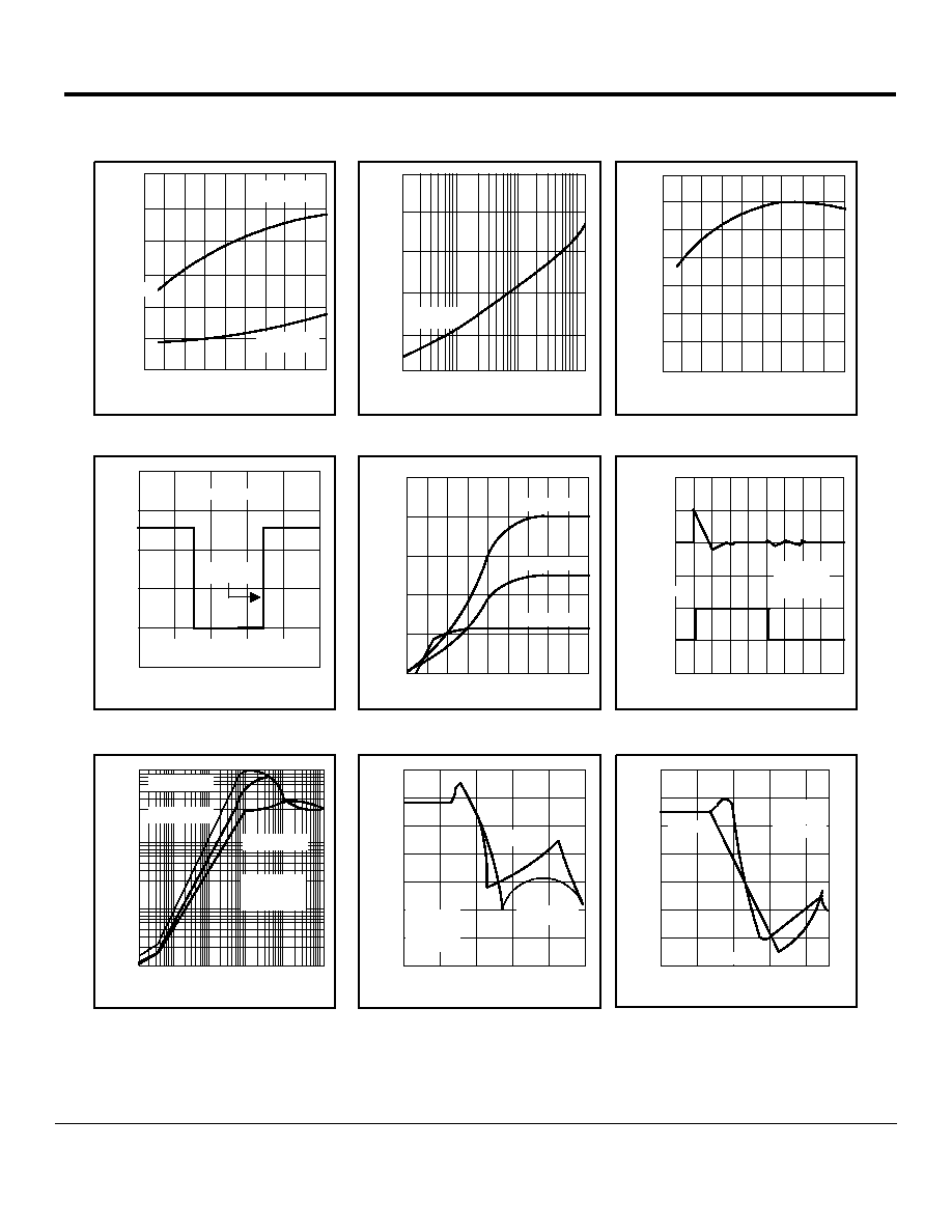
LP2950/ LP2951
TYPICAL PERFORMANCE CHARACTERISTIC
8
Rev. 8/10/01
LP2950/51 100mA Low Dropout Voltage Regulators
©Copyright 2001 Sipex Corporation
5
LP2951 Comparator Sink Current
S
I
N
K
C
U
R
R
E
N
T
(
m
A
)
2.5
1.5
OUTPUT LOW VOLTAGE (V)
2.0
1.0
0.5
0.0
0.0 0.1 0.2 0.3 0.4 0.5 0.6 0.7 0.8 0.9
T
A
= -55∫C
T
A
= 25∫C
T
A
= 125∫C
Line Transient Response
TIME(
µ
s)
100
0
200
400
600
800
I
N
P
U
T
O
U
T
P
U
T
V
O
L
T
A
G
E
V
O
L
T
A
G
E
C
H
A
N
G
E
4V
6V
8V
-50
0
50
~
~
mV
mV
mV
C
L
= 1
µ
F
I
L
= 1mA
V
OUT
= 5V
Error Comparator Output
C
O
M
P
A
R
A
T
O
R
O
U
T
P
U
T
(
V
)
8
6
0
INPUT VOLTAGE (V)
4
2
0
-2
1
2
3
4
5
V
OUT
= 5V
PULLUP RESISTOR TO
SEPARATE 5V SUPPLY
HYSTERESIS
Output Impedance
10
0.5
0.1
0.02
10
100
1K
10K
100K
1M
FREQUENCY (Hz)
O
U
T
P
U
T
I
M
P
E
D
A
N
C
E
(
O
H
M
S
)
5
0.2
0.05
0.01
1
2
I
O
= 100mA
I
O
= 100
µ
A
I
O
= 1mA
V
OUT
= 5V
C
L
= 1
µ
F
Ripple Rejection
90
70
60
40
10
1
10
2
10
3
10
4
10
5
10
6
FREQUENCY (Hz)
R
I
P
P
L
E
R
E
J
E
C
T
I
O
N
(
d
B
)
80
50
20
30
I
L
= 100
µ
A
I
L
= 0
C
L
= 1
µ
F
V
IN
= 6V
V
OUT
= 5V
Ripple Rejection
FREQUENCY (Hz)
R
I
P
P
L
E
R
E
J
E
C
T
I
O
N
(
d
B
)
10
6
10
3
10
2
10
1
90
80
70
60
50
20
40
30
10
4
10
5
I
L
= 10mA
I
L
= 1mA
C
L
= 1
µ
F
V
IN
= 6V
V
OUT
= 5V
Drop-Out Voltage
600
400
300
50
-75 -50 -25
0
25 50 75 100 125 150
TEMPERATURE (∫C)
D
R
O
P
-
O
U
T
V
O
L
T
A
G
E
(
m
V
)
500
100
0
I
L
= 100mA
I
L
= 100
µ
A
~
~
Drop-Out Voltage
T
J
= 25∫C
OUTPUT CURRENT
D
R
O
P
-
O
U
T
V
O
L
T
A
G
E
(
m
V
)
100mA
10mA
1mA
100
µ
A
500
400
300
200
100
0
Short Circuit Current
S
H
O
R
T
C
I
R
C
U
I
T
C
U
R
R
E
N
T
(
m
A
)
170
150
130
110
-75 -50 -25
0
25 50 75 100 125 150
TEMPERATURE (∫C)
160
140
120
110
LP2950/LP2951
TYPICAL PERFORMANCE CHARACTERISTICS (continued)