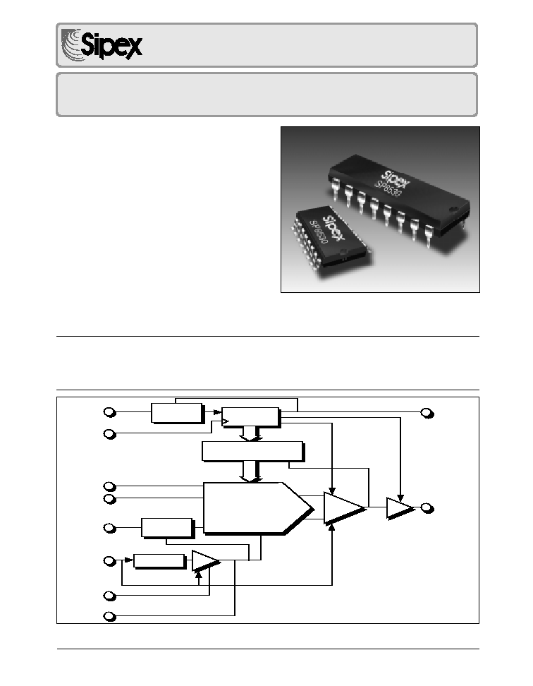
SP8530DS/01 SP8530 S
2
ADC
TM
- Simultaneous Sampling Analog to Digital Converter
© Copyright 2000 Sipex Corporation
1
s
Patented Simultaneous Sampling of
2 channels (Patent # 5,638,072)
s
12 Bit Resolution
s
Single +5Volt Supply
s
Internal Reference, 1.25V
s
Unipolar 0 to +2.5 Volt Input Range
s
Fast, 7.75
µ
s Conversion Time Both
Channels
SP8530
S
2
ADCTM - Simultaneous Sampling
Analog to Digital Converter
s
Fast Power Shutdown/Turn-On Mode
s
3-Wire Synchronous Serial High Speed
Interface
s
True Differential Measurements
s
2
µ
A Shutdown Mode (10
µ
W)
s
Low Power CMOS 60mW typical
DESCRIPTION
The SP8530 is a two channel simultaneous sampling, 12-Bit serial out data acquisition system.
The device contains a high speed 12-Bit analog to digital converter, internal reference, and
sample/hold circuitry for both channels. The 8530 is available in 16-pin PDIP and SOIC packages,
specified over Commercial and Industrial temperature ranges.
TM-S
2
ADC is a TRADEMARK OF SIPEX CORPORATION Patent Pending
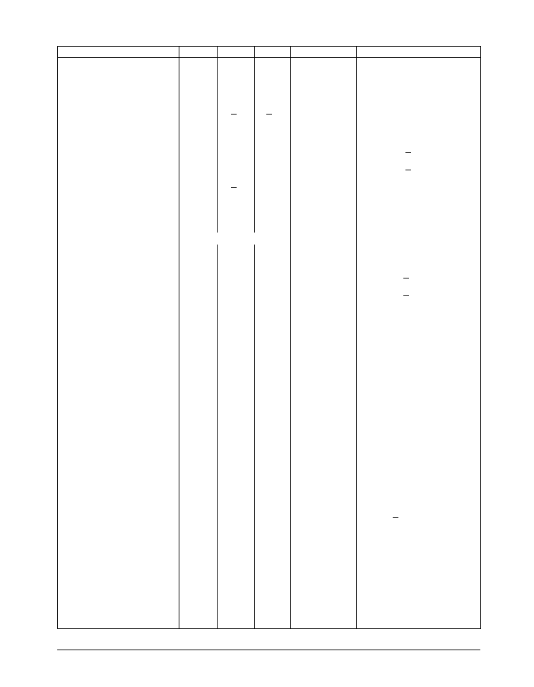
CONTROL
LOGIC
COUNTER
SAR
DAC
LATCHED
COMPARATOR
BUFFER
STATUS
D
OUT
REF.
CS
SCLK
V
IN
A
V
IN
B
OFFSET
ADJUST
PD
GAIN
ADJUST
REF OUT
RTRIM
Æ

SP8530DS/01 SP8530 S
2
ADC
TM
- Simultaneous Sampling Analog to Digital Converter
© Copyright 2000 Sipex Corporation
2
ABSOLUTE MAXIMUM RATINGS
(TA=+25∞C unless otherwise noted) ..............................................
VDD to DGND ............................................................. -0.3V to +7V
VDA to AGND .............................................................. -0.3V to +7V
Vin to AGND .................................................... -0.3V to VDA +0.3V
Digital Input to VSS ........................................... -0.3V to VDD+0.3V
Digital Output to VSS ........................................ -0.3V to VDD+0.3V
Operating Temp. Range
Commercial (J,K Version) ............................... 0∞C to 70∞C
Industrial (A,B Version) .............................. -40∞C to +85∞C
Storage Temperature ............................................... -65∞C to 150∞C
Lead Temperature(Solder 10sec) ........................................ +300∞C
Power Dissipation to +70∞C ................................................ 500mW
Derate Above 70∞C ......................................................... 10mW/ ∞C
SPECIFICATIONS
Unless otherwise noted the following specifications apply for V
DD
= 5V with limits applicable for T
A
= 25
o
C.
PARAMETER
MIN.
TYP.
MAX.
UNIT
CONDITIONS
DC Accuracy
Resolution
12
Bits
Integral Linearity
J, A
+0.6
+1.0
LSB
K ,B
+0.4
+0.75
LSB
Differential Linearity Error
J, A
+0.5
+1.0
LSB
No Missing Codes
K ,B
+0.5
+1.0
LSB
No Missing Codes
Gain Error
J, A
+0.2
+1.0
%FSR
Externally Trimmable to Zero
K,B
+0.1
+0.5
%FSR
Externally Trimmable to Zero
Offset Error
J, A
+4
+7
LSB
Externally Trimmable to Zero
K,B
+3
+5
LSB
Externally Trimmable to Zero
Gain Match
J, A
+2
LSB
K,B
+2
LSB
Offset Match
J, A
+1.0
LSB
Externally Trimmable to Zero
K,B
+0.5
LSB
Externally Trimmable to Zero
Analog Input
0 to 2.5
Volts
Conversion Speed
Sample Time
400
ns
Conversion Time
7.75
µ
s
Complete Cycle
8.25
Simultaneous Convert
Rate:
121
KHz
Simultaneous Pair
Clock Speed
4
MHz
Data Rate:
242
KHz
Total Data Conversion Rate
SP8530DS/01 SP8530 S
2
ADC
TM
- Simultaneous Sampling Analog to Digital Converter
© Copyright 2000 Sipex Corporation
3
SPECIFICATIONS
(continued)
Unless otherwise noted the following specifications apply for V
DD
= 5V with limits applicable for T
A
= 25
o
C.
PARAMETER
MIN.
TYP.
MAX.
UNIT
CONDITIONS
Reference Output
Ref. Out Temp. Coef.
1.25
Volt.Nom.
J, A
15
ppm/∞C
K,B
10
ppm/∞C
Ref.Out Error
+2
+25
mV
Output Current
1
mA
Digital Inputs
Input Low Voltage , VIL
0.8
Volt Max.
VDD
=
5V +5%
Input High Voltage , VIH
2.0
Volt Min.
VDD
=
5V +5%
Input Current IIN
+1
µ
A
Input Capacitance
3
pF Max.
Digital Outputs
Data Format
12-Bit Serial
See Timing diagram
Data Coding
Binary
See Timing Diagram
VOH
4.0
Volt. Min.
VDD=5V+5%, IOH=-0.4mA
VOL
0.4
Volt Max.
VDD=5V+5%, IOL=-1.6mA
AC Accuracy
fin=47KHz,VDD=5.0V
@ 25∞C, SCLK=4MHz
Spurious Free Dynamic
83
dB
Range (SFDR)
Total Harmonic Distortion
(THD)
-80
dB
Signal to Noise &
Distortion (SINAD)
71
dB
Signal to Noise (SNR)
72
dB
Sampling Dynamics
Acquisition Time to 0.01%
200
ns
For a +FS step change at
input
-3db Small Signal BW
13
MHz
Aperture Delay
35
ns
Aperture Jitter
150
ps RMS
Aperture Delay Matching
400
ps
Power Supplies
VDD
4.75
5.25
Volts

SP8530DS/01 SP8530 S
2
ADC
TM
- Simultaneous Sampling Analog to Digital Converter
© Copyright 2000 Sipex Corporation
4
SPECIFICATIONS
(continued)
Unless otherwise noted the following specifications apply for V
DD
= 5V with limits applicable for T
A
= 25
o
C.
PARAMETER
MIN.
TYP.
MAX.
UNIT
CONDITIONS
Power Supplies Cont.
Supply Current
Operating Mode
11.5
17
mA
SD=0, VDD=+5.0V
Shutdown Mode
0.01
2
µ
A
SD=1
Power Dissipation
Operating Mode
60
85
mW
SD=0
Shutdown Mode
.05
10
µ
W
SD=1
Power Turn On
20
µ
S
Via Shutdown Control
to 1 LSB settling error.
Temperature Range
Commercial
0
to
+70
∞C
Industrial
-40
to
+85
∞C
Storage
-65
to
+150
∞C

SP8530DS/01 SP8530 S
2
ADC
TM
- Simultaneous Sampling Analog to Digital Converter
© Copyright 2000 Sipex Corporation
5
time, thus preserving the relevant temporal
information of the applied signals, precisely.
This unique feature permits the SP8530 to
ideally fit applications where the information
content is carried on dual carriers, such as
in-phase and quadrature phase systems.
Further, S
2
ADCTM architecture permits the
sampling of such signals without the necessity
of demodulating or further conditioning of the
carrier prior to conversion, potentially saving
significant amounts of other support electronics.
It is also suited to measure instantaneous
transfer functions between input signals and
their corresponding output signal.
Such measurements are commonly made in test
equipment and PIN electronics as well as in
many other systems where instantaneous cause
and effect relationships are monitored.
The SP8530 permits the user to convert each
channel and digitally subtract the result in
external logic to produce a precise digital
differential result.
The SP8530 is fabricated in Sipex' Bipolar
Enhanced CMOS Process that permits state-of-
the-art design using bipolar devices in the
analog/linear section and extremely low power
CMOS in digital/logic section.
CIRCUIT OPERATION
The operating circuit in Figure 1 shows a simple
circuit required to operate the SP8530. The
conversion is controlled by the user supplied
signal Chip Select Bar (CS) which selects and
deselects the device, and a system clock (SCLK).
A high level applied to CS asynchronously
clears the internal logic, puts the sample & hold
(CDAC) into sample mode and places the DOUT
(Data Output) pin in a high impedance state.
Conversion is initiated by falling edge on CS in
slave mode at which point the selected input
voltages are held and a conversion is started. A
delay of 90ns is required between the falling
edge of CS and the first rising of SCLK.
FEATURES
The SP8530 is a two channel simultaneous
sampling, 12-Bit serial out data acquisition
system. The device contains a high speed 12-bit
analog to digital converter, internal reference,
and sample and hold circuitry for both channels.
The patented, simultaneous sampling feature of
this monolithic integrated circuit, permits the
user to measure and convert the analog
information on each of two channels at the same
PIN ASSIGNMENTS
Pin 1-N.C.-No Connection
Pin 2-VIN B-Analog Input B
Pin 3-VIN A- Analog Input A
Pin 4-AGND-Analog Ground
Pin 5-VSS-Digital Ground
Pin 6-SCLK-Serial Clock Input
Pin 7-DOUT Digital Data Output
Pin 8-STATUS- High During Conversion
Pin 9-CS-Chip Select Bar Input High Deselects
chip Low Selects chip
Pin 10-SD-Shutdown Input, logic low power
up, logic high = powerdown
Pin 11-VDD Digital +5V supply
Pin 12-VDA Analog +5V supply
Pin 13-OffADJ-A External Offset Adjust A
Pin 14-OffADJ-B External Offset Adjust B
Pin 15-REFOUT-Voltage Reference Output
Pin 16-GAINADJ-External Gain Adjustment
16
15
14
13
12
11
10
9
GAIN ADJUST
REF OUT
OFFSET ADJ. B
OFFSET ADJ. A
V
DA
V
DD
PD
CS
1
2
3
4
5
6
7
8
N.C.
V
IN
B
V
IN
A
AGND
V
SS
SCLK
D
OUT
STATUS
SP8530