 | –≠–ª–µ–∫—Ç—Ä–æ–Ω–Ω—ã–π –∫–æ–º–ø–æ–Ω–µ–Ω—Ç: SP2026 | –°–∫–∞—á–∞—Ç—å:  PDF PDF  ZIP ZIP |
1
Rev. 1/23/02 SP2026 +2.7V to +5.5V USB Power Control Switch © Copyright 2002 Sipex Corporation
PRELIMINARY
INFORMATION
s
Compliant to USB Specifications
s
+2.7V to +5.5V Input Voltage Range
s
Two Independent Power Switches
s
Two Error Flag Outputs, Open Drain
s
2.4V Undervoltage Lockout
s
500mA Minimum Continuous Load
Current Per Switch
s
1.25A Short Circuit Current Limit
s
140m
Maximum On-Resistance
SP2026
DESCRIPTION
The SP2026 is a dual +2.7V to +5.5V supervisory power control switch that is current limited
to 1.25A and has thermal shutdown to protect itself and the load. A device is disabled in
thermal shutdown until the excessive current load is removed, the appropriate enable pins are
toggled, or the die temperature cools to 120
∞
C. The undervoltage lockout feature disables the
output switches until a valid input voltage, V
IN
= 2.4V, is present. Once a valid input voltage
is present and the SP2026 is enabled, a 1ms soft start prevents momentary voltage drops
caused by charging a capacitive load. The SP2026 has a low on resistance, 100m
, and
supplies a 500mA minimum output current per switch. In overcurrent and thermal shutdown,
error flags may be asserted for overtemperature.
+2.7V to +5.5V USB Power Control Switch
Æ
s
100
µ
A On-State Supply Current
s
1
µ
A Shutdown Current
s
Output Can Be Forced Higher Than
Input (Off-State)
s
Thermal Shutdown
s
1ms Soft-Start Power Up
s
Active-High Version: SP2026-1
s
Active-Low Version: SP2026-2
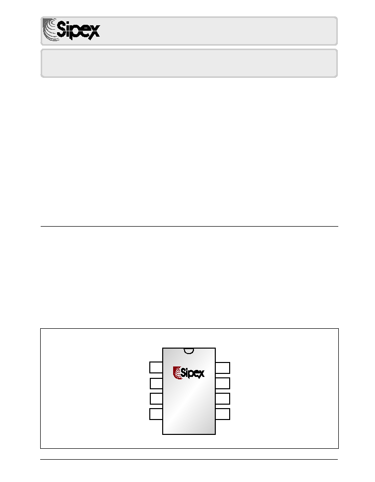
ENA
GND
OUTA
FLGA
FLGB
OUTB
IN
ENB
8
7
4
3
2
1
5
6
SP2026
Æ
Æ
2
Rev. 1/23/02 SP2026 +2.7V to +5.5V USB Power Control Switch © Copyright 2002 Sipex Corporation
PRELIMINARY
INFORMATION
ABSOLUTE MAXIMUM RATINGS
These are stress ratings only and functional operation
of the device at these ratings or any other above those
indicated in the operation sections of the specifica-
tions below is not implied. Exposure to absolute maxi-
mum rating conditions for extended periods of time
may affect reliability.
Supply Voltage ..................................... -0.3V, +6.0V
Operating Temperature .................... -40∞C to +85∞C
Storage Temperature ..................... -65∞C to +150∞C
Power Dissipation Per Package
8-pin NSOIC
(derate 6.14mW/
O
C above+70
O
C) ................ 500mW
PARAMETER
MIN.
TYP.
MAX. UNITS CONDITIONS
Operating Voltage Range, V
IN
2.7
5.5
V
Supply Current, I
IN
0.75
5.0
µ
A
enable off, no output load
100
160
µ
A
enable on, no output load
Enable Input Threshold Voltage
1.7
2.4
V
low to high transition
0.8
1.45
V
high to low transition
Enable Input Current
-1.0
0.01
1.0
µ
A
V
EN
= 0V to 5.5V
Enable Input Capacitance
1
pF
Switch Resistance
90
140
m
V
IN
= 5V, I
OUT
= 500mA
100
170
m
V
IN
= 3.3V, I
OUT
= 500mA
Output Turn-On Delay
1.3
5.0
ms
RL =10
each output, CL = 1
µ
F
Output Turn-On Rise Time
1.15
4.9
ms
R
L
=10
each output, C
L
= 1
µ
F
Output Turn-Off Delay
35
100
µ
s
R
L
=10
each output, C
L
= 1
µ
F
Output Turn-Off Fall Time
32
100
µ
s
R
L
=10
each output, C
L
= 1
µ
F
Output Leakage Current
10
µ
A
V
ENX
0.8V
Current Limit Threshold
1.0
1.25
A
ramped load applied to output
Short Circuit Current Limit
0.5
0.9
1.25
A
each output, V
OUT
= 0V
Over-Temperature Shutdown
140
∞
C
temperature increasing each switch
Threshold
120
∞
C
temperature decreasing each switch
160
∞
C
temperature increasing both switches
150
∞
C
temperature decreasing both switches
Error Flag Output Resistance
10
25
V
IN
= 5V,I
L
=10mA
15
40
V
IN
= 3.3V,I
L
=10mA
Error Flag Off Current
10
µ
A
V
FLAG
= 5V
UVLO Threshold
2.2
2.4
2.7
V
V
IN
increasing, T
MIN
to T
MAX
2.0
2.15
2.3
V
V
IN
decreasing T
MIN
to T
MAX
Enable Input Hysteresis
250
mV
Off Current in Latched Thermal
50
During thermal shutdown state
Shutdown
Short Circuit Response Time
20
µ
s
V
OUT
= 0V to I
OUT
= 1 limit
Overcurrent Flag Response Delay
1.5
3.0
7.0
ms
V
IN
= 5V, apply V
OUT
= 0V until FLG low
3.0
ms
V
IN
= 3.3V, apply V
OUT
= 0V until FLG low
SPECIFICATIONS
Unless otherwise noted, the following specifications apply for V
IN
= +5.0V, T
A
= 25
∞
C.
8-pin PDIP
(derate 11.8mW/
O
C above+70
O
C). ............. 1000mW
Fault Flag Voltage ............................................. +6V
Fault Flag Current ........................................... 25mA
Output Voltage .................................................. +6V
Output Current .............................. Internally Limited
Enable Input .................................. -0.3V to VIN +3V

3
Rev. 1/23/02 SP2026 +2.7V to +5.5V USB Power Control Switch © Copyright 2002 Sipex Corporation
PRELIMINARY
INFORMATION
PIN ASSIGNMENTS
PIN NUMBER
PIN SYMBOL
DESCRIPTION
1
ENA
Enable Input for MOSFET Switch A. This input pin is active
high for the SP2026-1 and active low for the SP2026-2.
2
FLGA
Fault Flag Output for Switch Channel A. This open drain
output pin pulls low to indicate overcurrent and thermal
shutdown conditions.
3
FLGB
Fault Flag Output for Switch Channel B. This open drain
output pin pulls low to indicate overcurrent and thermal
shutdown conditions.
4
ENB
Enable Input for MOSFET Switch B. This input pin is active
high for the SP2026-1 and active low for the SP2026-2.
5
OUTA
Output for MOSFET Switch Channel A. This is the output pin
of the MOSFET source of channel A, typically connected to
the switched side of the load.
6
GND
Ground reference. Supply return.
7
IN
Supply Input. This input pin is connected to the MOSFET drain
of both switches. Connect +2.7V to +5.5V to this input pin.
The voltage at this input pin also supplies the internal circuitry.
8
OUTB
Output for MOSFET Switch Channel B. This is the output pin
of the MOSFET source of channel B, typically connected to the
switched side of the load.
ENA
GND
OUTA
FLGA
FLGB
OUTB
IN
ENB
8
7
4
3
2
1
5
6
SP2026
Æ
Æ

4
Rev. 1/23/02 SP2026 +2.7V to +5.5V USB Power Control Switch © Copyright 2002 Sipex Corporation
PRELIMINARY
INFORMATION
FEATURES
Features of the SP2026 device include current
limiting, a +2.4V undervoltage lockout,
overtemperature shutdown, error flag output,
soft start, a switch-on resistance of 100m
and
a supply current of 100
µ
A. The SP2026-1 de-
vice has an active-high enable. The SP2026-2
device has an active-low enable.
THEORY OF OPERATION
The SP2026 is a dual integrated high-side power
switch optimized for self-powered and bus-
powered Universal Serial Bus (USB) applica-
tions. There are operational conditions that will
enable or disable one or more of the output
MOSFET switches, depending on the type of
hazard. Certain conditions will activate the
open-drain error flag transistors forcing the flag
outputs to ground. The SP2026 provides the
following functions:
1) Independent Solid State Switches: Indepen-
dent MOSFET switches connect the IN pin to
the OUTA and OUTB pins when enabled by
logic signals at the ENA and ENB control pins.
2) Fault Flag Conditions: Both the FLGA and
FLGB pins are N-channel, open-drain MOSFET
outputs capable of sinking a 10mA load to
typically 100mV above ground.
3) Undervoltage Lockout: The lockout mecha-
nism monitors the input voltage and will enable
the MOSFET switches only when the voltage at
the V
IN
pin is greater than +2.4V.
4) Current Limiting Threshold: A current
limiting threshold prevents damage to the de-
vice and external load.
5) Thermal Shutdown: The SP2026 has dual
sensors to detect overtemperature. If the die
temperature reaches 140
∞
C and channel A is in
current limit, output switch A is disabled and
flag A is asserted. Unless channel B current
limits, switch B remains enabled and flag B is
not asserted. If the die temperature reaches
140
∞
C and channel B is in current limit, output
switch B is disabled and flag B is asserted.
Unless channel A current limits, switch A re-
mains enabled and flag A is not asserted. If the
die exceeds 160
∞
C, both output switches are
disabled and both flags are asserted. A device is
disabled in thermal shutdown until the excessive
current load is removed, the appropriate enable pins
are toggled, or the temperature cools to 120
∞
C.
Input and Output
The independent solid state MOSFET switches
connect the USB +5.0V supply voltage at the IN
pin to the OUTA and OUTB pins when enabled
by logic signals at ENA and ENB. The IN pin is
the power supply connection to the device and the
drain of the output MOSFET switches.
Typically, the current will flow through the
switches from IN to OUTA and OUTB towards
the load. If V
OUT
is greater than V
IN
when a switch
is enabled, the current will flow from OUTA or
OUTB to the IN pin because the MOSFET chan-
nels are bidirectional when switched on.
Under normal operating condition, the MOSFET
switches will present 100m
resistance when
closed. The output MOSFETs and driver cir-
cuitry are designed to allow the MOSFET source
to be externally forced to a higher voltage than the
drain when the switch is off.
Fault Flag Conditions
Fault conditions disable one or both MOSFET
switches, depending on the type of fault. FLGA
and FLGB are N-channel, open-drain MOSFET
outputs. The active low fault flag occurs when
one of the following conditions exist:
1. Overcurrent
2. Overtemperature
Undervoltage Lockout
This voltage lockout mechanism prevents the
MOSFET switches from turning on until V
IN
is
greater than +2.4V.
After the switch turns on, if the voltage at V
IN
drops below +2.15V, the lockout circuitry shuts
off both switches. This detection functions only
when at least one MOSFET switch is enabled.
Output Current Limiting
The SP2026 has a preset current-limit threshold.
These switch control circuits will implement cur-
rent limiting which prevents damage to the SP2026
and the external load while allowing a minimum
current of 0.5A to be delivered to the load.

5
Rev. 1/23/02 SP2026 +2.7V to +5.5V USB Power Control Switch © Copyright 2002 Sipex Corporation
PRELIMINARY
INFORMATION
Figure 1. Internal Block Diagram for the SP2026
M4
M3
M1
M2
ENA
FLAGA
GND
OUTA
GND
FLAGB
OUTB
GND
ENB
V
REF
UVLO
OVER TEMPERATURE 140∞C
SHUT DOWN B
SHUT DOWN A
COMPARATOR
VOLTAGE
REFERENCE
AND
TEMPERATURE
SENSING
FOLDBACK
B
CHARGE
PUMP
B
OSCILLATOR
B
LOGIC B
GND
IN
1
2
3
4
6
6
6
6
8
7
5
SP2026
Æ
Æ
CURRENT
SENSE
OVER TEMPERATURE 160∞C
OVERCURRENT
OVERCURRENT
CURRENT
SENSE
FOLDBACK
A
CHARGE
PUMP
A
OSCILLATOR
A
OVERCURRENT
CHANNEL B
OVERTEMPERATURE
140∞C
OVERTEMPERATURE
160∞C
LOGIC A
OVERCURRENT
CHANNEL A
OVERTEMPERATURE
140∞C
OVERTEMPERATURE
160∞C