 | –≠–ª–µ–∫—Ç—Ä–æ–Ω–Ω—ã–π –∫–æ–º–ø–æ–Ω–µ–Ω—Ç: SP503CF | –°–∫–∞—á–∞—Ç—å:  PDF PDF  ZIP ZIP |

1
Date: 7/29/04
SP503 Multiprotocol Transceiver
© Copyright 2004 Sipex Corporation
Single Chip Programmable Serial
Transceiver
Seven (7) Drivers and Seven (7)
Receivers
Software-Selectable Industry Standard
Protocols:
-- RS-232 (V.28)
-- EIA-530
-- RS-449
-- RS-422A (V.11, X.27)
-- RS-485
-- V.35
Independant Driver and Receiver Mode
Selection
+5V Single Power Supply Operation
Surface Mount Packaging
SP503
Charge
Pump
Receiver
Decode
Driver
Decode
Receivers
Drivers
DESCRIPTION
The SP503 is a highly integrated serial transceiver that allows software control of its interface
modes. It offers hardware interface modes for RS-232 (V.28), RS-422A (V.11), RS-449, RS-485,
V.35, and EIA-530. The SP503 is fabricated using low≠power BiCMOS process technology, and
incorporates a Sipex patented (5,306,954) charge pump allowing +5V only operation.
SP503
Multiprotocol Transceiver
Æ
Now Available in Lead Free Packaging
RxD 1
RDEC
0
2
RDEC
1
3
RDEC
2
4
RDEC
3
5
TTEN 6
SCTEN 7
V
CC
8
TDEC
3
9
TDEC
2
10
TDEC
1
11
TDEC
0
12
DTR 13
TxD 14
TxC 15
RTS 16
RL 17
NC 18
DCD 19
RxC 20
RI 21
ST 22
STEN 23
LL 24
V
CC
25
C
1
+
26
V
DD
27
C
2
+
28
GND 29
C
1
≠
30
C
2
≠
31
V
SS
32
V
CC
33
GND 34
RR(a) 35
RR(b) 36
RT(a) 37
RT(b) 38
IC(a) 39
IC(b) 40
60 GND
59 SD(b)
58 TR(a)
57 GND
56 TR(b)
55 V
CC
54 RS(a)
53 GND
52 RS(b)
51 LL(a)
50 GND
49 LL(b)
48 V
CC
47 RL(a)
46 GND
45 RL(b)
44 ST(b)
43 GND
42 ST(a)
41 V
CC
80 CTS
79 SCT
78 DSR
77
SCT(b)
76 SCT(a)
75 GND
74 V
CC
73 V
CC
72 GND
71 RD(b)
70 RD(a)
69 DM(b)
68 DM(a)
67 CS(b)
66 CS(a)
65 TT(b)
64 GND
63 TT(a)
62 V
CC
61 SD(a)
SP503

Date: 7/29/04
SP503 Multiprotocol Transceiver
© Copyright 2004 Sipex Corporation
2
ELECTRICAL CHARACTERISTICS
T
MIN
to T
MAX
@ Vcc = +5V ±5% unless otherwise noted.
MIN.
TYP.
MAX.
UNITS
CONDITIONS
LOGIC INPUTS
V
IL
0.8
Volts
V
IH
2.0
Volts
LOGIC OUTPUTS
V
OL
0.4
Volts
I
OUT
= -3.2mA
V
OH
2.4
Volts
I
OUT
= 1.0mA
RS-485 DRIVER
TTL Input Levels
V
IL
0.8
Volts
V
IH
2.0
Volts
Outputs
HIGH Level Output
+6.0
Volts
LOW level Output
≠0.3
Volts
Differential Output
±1.5
±5.0
Volts
R
L
=54, C
L
=50pF
Balance
±0.2
Volts
|V
T
| - |V
T
|
Open Circuit Voltage
±6.0
Volts
Output Current
28.0
mA
R
L
=54
Short Circuit Current
±250
mA
Terminated in ≠7V to +12V
Transition Time
120
ns
Rise/fall time, 10%≠90%
Maximum Transmission Rate
5
Mbps
R
L
=54
Propagation Delay
t
PHL
200
ns
R
L
=54
t
PLH
200
ns
R
L
=54
RS-485 RECEIVER
TTL Output Levels
V
OL
0.4
Volts
V
OH
2.4
Volts
Input
HIGH Threshold
+0.2
+12.0
Volts
(a)-(b)
LOW Threshold
≠7.0
≠0.2
Volts
(a)-(b)
Common Mode Range
≠7.0
+12.0
Volts
HIGH Input Current
Refer to graph
LOW Input Current
Refer to graph
Receiver Sensitivity
±0.2
Volts
Over ≠7V to +12V common
mode range
Input Impedance
12
k
Maximum Transmission Rate
5
Mbps
Propagation Delay
t
PHL
200
ns
t
PLH
200
ns
V.35 DRIVER
TTL Input Levels
V
IL
0.8
Volts
V
IH
2.0
Volts
Outputs
Differential Output
±0.44
±0.66
Volts
With termination network in
Figure 6; R
L
=100
Output Impedance
50
150
With termination network in
Figure 6.
Short Circuit Impedance
135
150
165
With termination network
in Figure 6.
Transition Time
40
ns
Maximum Transmission Rate
5
Mbps
R
L
=100
Propagation Delay
t
PHL
200
ns
R
L
=100
t
PLH
200
ns
R
L
=100

3
Date: 7/29/04
SP503 Multiprotocol Transceiver
© Copyright 2004 Sipex Corporation
ELECTRICAL CHARACTERISTICS
T
MIN
to T
MAX
@ Vcc = +5V ±5% unless otherwise noted.
MIN.
TYP.
MAX.
UNITS
CONDITIONS
V.35 RECEIVER
TTL Output Levels
V
OL
0.4
Volts
V
OH
2.4
Volts
Input
Receiver Sensitivity
±0.2
Volts
Input Impedance
90
100
110
With termination network
in Figure 6.
Short Circuit Impedance
135
150
165
With termination network
in Figure 6.
Maximum Transmission Rate
5
Mbps
Propagation Delay
t
PHL
200
ns
t
PLH
200
ns
RS-422 DRIVER
TTL Input Levels
V
IL
0.8
Volts
V
IH
2.0
Volts
Outputs
Differential Output
±2.0
±5.0
Volts
R
L
=100
Open Circuit Voltage,V
O
±6.0
Volts
Balance
±0.4
Volts
|V
T
| ≠ |V
T
|
Offset
+3.0
Volts
Short Circuit Current
±150
mA
V
OUT
=0V
Power Off Current
±100
µA
V
cc
= 0V, V
out
= ±0.25V
Transition Time
60
ns
Rise/fall time, 10%-90%
Maximum Transmission Rate
5
Mbps
R
L
=100
Propagation Delay
t
PHL
200
ns
R
L
=100
t
PLH
200
ns
R
L
=100
RS-422 RECEIVER
TTL Output Levels
V
OL
0.4
Volts
V
OH
2.4
Volts
Input
HIGH Threshold
+0.2
+6.0
Volts
(a)-(b)
LOW Threshold
≠6.0
≠0.2
Volts
(a)-(b)
Common Mode Range
≠7.0
+7.0
Volts
HIGH Input Current
Refer to graph
LOW Input Current
Refer to graph
Receiver Sensitivity
±0.2
Volts
V
CM
=+7V to -7V
Input Impedance
4
k
V
CM
=+10V to -10V
Maximum Transmission Rate
5
Mbps
Propagation Delay
t
PHL
200
ns
t
PLH
200
ns
RS-232 DRIVER
TTL Input Level
V
IL
0.8
Volts
V
IH
2.0
Volts
Outputs
HIGH Level Output
+5.0
+15
Volts
R
L
=3k, V
IN
=0.8V, V
cc
= 5V
LOW Level Output
≠15.0
≠5.0
Volts
R
L
=3k, V
IN
=2.0V, V
cc
= 5V
Open Circuit Voltage
≠15
+15
Volts
Short Circuit Current
±100
mA
V
OUT
=0V
Power Off Impedance
300
V
cc
= 0V, V
out
= ±2.0V

Date: 7/29/04
SP503 Multiprotocol Transceiver
© Copyright 2004 Sipex Corporation
4
ELECTRICAL CHARACTERISTICS
T
MIN
to T
MAX
@ Vcc = +5V ±5% unless otherwise noted.
MIN.
TYP.
MAX.
UNITS
CONDITIONS
Slew Rate
30
V/µs
R
L
=3k, C
L
=15pF
Transition Time
1.56
µs
R
L
=3k, C
L
=2500pF
Maximum Transmission Rate
120
kbps
R
L
=3k, C
L
=2500pF
Propagation Delay
t
PHL
2
8
µs
R
L
=3k
t
PLH
2
8
µs
R
L
=3k
RS-232 RECEIVER
TTL Output Levels
V
OL
0.4
Volts
V
OH
2.4
Volts
Input
HIGH Threshold
1.7
2.4
Volts
LOW Threshold
0.8
1.2
Volts
Receiver Open Circuit Bias
+2.0
Volts
Input Impedance
3
5
7
k
V
IN
=+15V to -15V
Maximum Transmission Rate
120
kbps
Propagation Delay
t
PHL
1
µs
t
PLH
1
µs
RS-423 DRIVER
TTL Input Levels
V
IL
0.8
Volts
V
IH
2.0
Volts
Output
Open Circuit Voltage
±4.0
±10.0
Volts
HIGH Level Output
+3.6
+6.0
Volts
R
L
=550
LOW Level Output
≠6.0
≠3.6
Volts
R
L
=550
Short Circuit Current
±150
mA
V
OUT
=0V
Power Off Current
±100
µA
V
cc
= 0V, V
out
= ±0.25V
Transition Time
0.8
2.4
µs
Rise/fall time, 10-90%
Maximum Transmission Rate
120
kbps
R
L
=550
Propagation Delay
t
PHL
2
8
µs
R
L
=550
t
PLH
2
8
µs
R
L
=550
RS-423 RECEIVER
TTL Output Levels
V
OL
0.4
Volts
V
OH
2.4
Volts
Input
HIGH Threshold
+0.2
+7.0
Volts
LOW Threshold
≠7.0
≠0.2
Volts
HIGH Input Current
Refer to graph
LOW Input Current
Refer to graph
Receiver Sensitivity
±0.2
Volts
V
CM
= +7V to -7V
Input Impedance
4
k
V
IN
= +10V to -10V
Maximum Transmission Rate
120
kbps
Propagation Delay
t
PHL
1
µs
t
PLH
1
µs
POWER REQUIREMENTS
V
CC
4.75
5.25
Volts
I
CC
20
30
mA
V
CC
=5V; no interface selected
ENVIRONMENTAL AND MECHANICAL
Operating Temperature Range
0
+70
∞C
Storage Temperature Range
≠65
+150
∞C
Package
80≠pin QFP

5
Date: 7/29/04
SP503 Multiprotocol Transceiver
© Copyright 2004 Sipex Corporation
V.35
47.0mA
48.8mA
47.3mA
54.5mA 104.2mA
100.9mA
100.9mA
RS-232
35.4mA
37.8mA
35.2mA
43.6mA
54.1mA
57.1mA
55.9mA
RS-422
25.8mA
31.4mA
25.8mA
27.5mA
140.2mA
135.9mA
145.2mA
RS-485
33.4mA
37.91mA
33.51mA
34.81mA
200.3mA
194.8mA
203.3mA
RS-449
37.8mA
40.3mA
41.1mA
42.9mA
142.3mA
138.8mA
147.4mA
EIA-530
45.2mA
48.1mA
44.4mA
50.3mA
148.9mA
145.7mA
147.3mA
+1.0mA
≠0.6mA
+12V
+6V
≠3V
≠7V
1 Unit Load
Maximum Input Current
versus Voltage
RS-485 RECEIVER
+3.25mA
≠3.25mA
+10V
+3V
≠3V
≠10V
Maximum Input Current
versus Voltage
RS-422 RECEIVER
+3.25mA
≠3.25mA
+10V
+3V
≠3V
≠10V
Maximum Input Current
versus Voltage
RS-423 RECEIVER
RECEIVER INPUT GRAPHS
POWER MATRIX
Mode Open Input Input to 5V Input to GND AC Signal Input to 5V Input to GND AC Signal
Conditions
to Input with Load with Load with Load
With external termination resistor network;
Input @ 60kHz, Load is 3k & 2500pF for
RS-232 and 100 for V.35
Input @ 60kHz
Load is 100 for RS-422
450 for RS-423
Input @ 60kHz
Load is 100 for RS-422
450 for RS-423
Input @ 2.5MHz
Load is 54.
Input @ 2.5MHz
Load is 100.
Input @ 60kHz
Load is 3k & 2500pF for RS-232.
Typical @ 25∞C and V
cc
= +5V unless otherwise noted. Input is applied to one driver.

Date: 7/29/04
SP503 Multiprotocol Transceiver
© Copyright 2004 Sipex Corporation
6
OTHER AC CHARACTERISTICS
(Typical @ 25∞C and nominal supply voltages unless otherwise noted)
PARAMETER
MIN.
TYP.
MAX.
UNITS
CONDITIONS
DELAY TIME FROM ENABLE MODE TO TRI≠STATE MODE
SINGLE≠ENDED MODE (RS-232, RS-423)
t
PZL
; Enable to Output LOW
190
ns
3k pull≠up to output
t
PZH
; Enable to Output HIGH
130
ns
3k pull≠down to output
t
PLZ
; Disable from Output LOW
270
ns
5V to input
t
PHZ
; Disable from Output HIGH
400
ns
GND to input
DIFFERENTIAL MODE (RS-422, RS-485, V.35)
t
PZL
; Enable to Output LOW
100
ns
3k pull≠up to output
t
PZH
; Enable to Output HIGH
100
ns
3k pull≠down to output
t
PLZ
; Disable from Output LOW
130
ns
5V to input
t
PHZ
; Disable from Output HIGH
140
ns
GND to input
Notes:
1.
Measured from 2.5V of R
IN
to 2.5V of R
OUT
.
2.
Measured from one≠half of R
IN
to 2.5V of R
OUT
.
3.
Measured from 1.5V of T
IN
to one≠half of T
OUT
.
4.
Measured from 2.5V of R
O
to 0V of A and B.
PINOUT...
RxD 1
RDEC
0
2
RDEC
1
3
RDEC
2
4
RDEC
3
5
TTEN 6
SCTEN 7
V
CC
8
TDEC
3
9
TDEC
2
10
TDEC
1
11
TDEC
0
12
DTR 13
TxD 14
TxC 15
RTS 16
RL 17
NC 18
DCD 19
RxC 20
RI 21
ST 22
STEN 23
LL 24
V
CC
25
C
1
+
26
V
DD
27
C
2
+
28
GND 29
C
1
≠
30
C
2
≠
31
V
SS
32
V
CC
33
GND 34
RR(a) 35
RR(b) 36
RT(a) 37
RT(b) 38
IC(a) 39
IC(b) 40
60 GND
59 SD(b)
58 TR(a)
57 GND
56 TR(b)
55 V
CC
54 RS(a)
53 GND
52 RS(b)
51 LL(a)
50 GND
49 LL(b)
48 V
CC
47 RL(a)
46 GND
45 RL(b)
44 ST(b)
43 GND
42 ST(a)
41 V
CC
80 CTS
79 SCT
78 DSR
77
SCT(b)
76 SCT(a)
75 GND
74 V
CC
73 V
CC
72 GND
71 RD(b)
70 RD(a)
69 DM(b)
68 DM(a)
67 CS(b)
66 CS(a)
65 TT(b)
64 GND
63 TT(a)
62 V
CC
61 SD(a)
SP503
PIN ASSIGNMENTS...
CLOCK AND DATA GROUP
Pin 1 -- RxD -- Receive Data; TTL output,
sourced from RD(a) and RD(b) inputs.
Pin 14 -- TxD -- TTL input ; transmit data
source for SD(a) and SD(b) outputs.
Pin 15 -- TxC -- Transmit Clock; TTL input for
TT driver outputs.
Pin 20 -- RxC -- Receive Clock; TTL output
sourced from RT(a) and RT(b) inputs.
Pin 22 -- ST -- Send Timing; TTL input; source
for ST(a) and ST(b) outputs.
Pin 37 -- RT(a) -- Receive Timing; analog
input, inverted; source for RxC.
Pin 38 -- RT(b) -- Receive Timing; analog
input, non-inverted; source for RxC.
Pin 42 -- ST(a) -- Send Timing; analog output,
inverted; sourced from ST.
Pin 44 -- ST(b) -- Send Timing; analog output,
non-inverted; sourced from ST.
Pin 59 -- SD(b) -- Analog Out -- Send data,
non-inverted; sourced from TxD.
Pin 61 -- SD(a) -- Analog Out -- Send data,
inverted; sourced from TxD.
Pin 63 -- TT(a) -- Analog Out -- Terminal
Timing, inverted; sourced from TxC
Pin 65 -- TT(b) -- Analog Out -- Terminal
Timing, non≠inverted; sourced from TxC.
Pin 70 -- RD(a) -- Receive Data, analog input;
inverted; source for RxD.

7
Date: 7/29/04
SP503 Multiprotocol Transceiver
© Copyright 2004 Sipex Corporation
Pin 71 -- RD(b) -- Receive Data; analog input;
non-inverted; source for RxD.
Pin 76 -- SCT(a) -- Serial Clock Transmit;
analog input, inverted; source for SCT.
Pin 77 -- SCT(b) -- Serial Clock Transmit:
analog input, non≠inverted; source for SCT
Pin 79 -- SCT -- Serial Clock Transmit; TTL
output; sources from SCT(a) and SCT(b) inputs.
CONTROL LINE GROUP
Pin 13 -- DTR -- Data Terminal Ready; TTL
input; source for TR(a) and TR(b) outputs.
Pin 16 -- RTS -- Ready To Send; TTL input;
source for RS(a) and RS(b) outputs.
Pin 17 -- RL -- Remote Loopback; TTL input;
source for RL(a) and RL(b) outputs.
Pin 19 -- DCD-- Data Carrier Detect; TTL
output; sourced from RR(a) and RR(b) inputs.
Pin 21 -- RI -- Ring In; TTL output; sourced
from IC(a) and IC(b) inputs.
Pin 24 -- LL -- Local Loopback; TTL input;
source for LL(a) and LL(b) outputs.
Pin 35 -- RR(a)-- Receiver Ready; analog
input, inverted; source for DCD.
Pin 36 -- RR(b)-- Receiver Ready; analog
input, non-inverted; source for DCD.
Pin 39 -- IC(a)-- Incoming Call; analog input,
inverted; source for RI.
Pin 40 -- IC(b)-- Incoming Call; analog input,
non-inverted; source for RI.
Pin 45 -- RL(b) -- Remote Loopback; analog
output, non-inverted; sourced from RL.
Pin 47 -- RL(a) -- Remote Loopback; analog
output inverted; sourced from RL.
Pin 49-- LL(b) -- Local Loopback; analog
output, non-inverted; sourced from LL.
Pin 51 -- LL(a) -- Local Loopback; analog
output, inverted; sourced from LL.
Pin 52 -- RS(b) -- Ready To Send; analog
output, non-inverted; sourced from RTS.
Pin 54 -- RS(a) -- Ready To Send; analog
output, inverted; sourced from RTS.
Pin 56 -- TR(b) -- Terminal Ready; analog
output, non-inverted; sourced from DTR.
Pin 58 -- TR(a) -- Terminal Ready; analog
output, inverted; sourced from DTR.
Pin 66 -- CS(a)-- Clear To Send; analog input,
inverted; source for CTS.
Pin 67 -- CS(b)-- Clear To Send; analog input,
non-inverted; source for CTS.
Pin 68 -- DM(a)-- Data Mode; analog input,
inverted; source for DSR.
Pin 69 -- DM(b)-- Data Mode; analog input,
non-inverted; source for DSR
Pin 78 -- DSR-- Data Set Ready; TTL output;
sourced from DM(a), DM(b) inputs.
Pin 80 -- CTS-- Clear To Send; TTL output;
sourced from CS(a) and CS(b) inputs.
CONTROL REGISTERS
Pins 2≠5 -- RDEC
0
≠ RDEC
3
-- Receiver
decode register; configures receiver modes; TTL
inputs.
Pin 6 -- TTEN -- Enables TT driver, active
low; TTL input.
Pin 7 -- SCTEN -- Enables SCT receiver;
active high; TTL input.
Pins 12≠9 -- TDEC
0
≠ TDEC
3
-- Transmitter
decode register; configures transmitter modes;
TTL inputs.
Pin 23 -- STEN -- Enables ST driver; active
low; TTL input.
POWER SUPPLIES
Pins 8, 25, 33, 41, 48, 55, 62, 73, 74 -- V
CC
--
+5V input.
Pins 29, 34, 43, 46, 50, 53, 57, 60, 64, 72, 75 --
GND -- Ground.
Pin 27 -- V
DD
+10V Charge Pump Capacitor --
Connects from V
DD
to V
CC
. Suggested capaci-
tor size is 22
µF, 16V.

Date: 7/29/04
SP503 Multiprotocol Transceiver
© Copyright 2004 Sipex Corporation
8
Pin 32 -- V
SS
≠10V Charge Pump Capacitor --
Connects from ground to V
SS
. Suggested ca-
pacitor size is 22
µF, 16V.
Pins 26 and 30 -- C
1
+
and C
1
≠
-- Charge Pump
Capacitor -- Connects from C
1
+
to C
1
≠
. Sug-
gested capacitor size is 22
µF, 16V.
Pins 28 and 31 -- C
2
+
and C
2
≠
-- Charge Pump
Capacitor -- Connects from C
2
+
to C
2
≠
. Sug-
gested capacitor size is 22
µF, 16V.
NOTE: NC pins should be left floating; internal
signals may be present.
pared to older less≠efficient designs. The charge
pump still requires four external capacitors, but
uses a four≠phase voltage shifting technique to
attain symmetrical 10V power supplies. Figure
3(a) shows the waveform found on the positive
side of capcitor C2, and Figure 3(b) shows the
negative side of capcitor C2. There is a free≠
running oscillator that controls the four phases
of the voltage shifting. A description of each
phase follows.
Phase 1
-- V
SS
charge storage --During this phase of
the clock cycle, the positive side of capacitors
C
1
and C
2
are initially charged to +5V. C
l
+
is
then switched to ground and the charge on C
1
≠
is
transferred to C
2
≠
. Since C
2
+
is connected to
+5V, the voltage potential across capacitor C
2
is now 10V.
Phase 2
-- V
SS
transfer -- Phase two of the clock con-
nects the negative terminal of C
2
to the V
SS
storage capacitor and the positive terminal of C
2
to ground, and transfers the generated ≠l0V to
C
3
. Simultaneously, the positive side of capaci-
tor C
1
is switched to +5V and the negative side
is connected to ground.
Phase 3
-- V
DD
charge storage -- The third phase of the
clock is identical to the first phase -- the charge
transferred in C
1
produces ≠5V in the negative
terminal of C
1
, which is applied to the negative
side of capacitor C
2
. Since C
2
+
is at +5V, the
voltage potential across C
2
is l0V.
Phase 4
-- V
DD
transfer -- The fourth phase of the
clock connects the negative terminal of C
2
to
ground and transfers the generated l0V across
C
2
to C
4
, the V
DD
storage capacitor. Again,
FEATURES...
The SP503 is a highly integrated serial trans-
ceiver that allows software control of its inter-
face modes. The SP503 offers hardware inter-
face modes for RS-232 (V.28), RS-422A (V.11),
RS-449, RS-485, V.35, and EIA-530. The inter-
face mode selection is done via an 8≠bit switch;
four (4) bits control the drivers and four (4) bits
control the receivers. The SP503 is fabricated
using low≠power BiCMOS process technology,
and incorporates a Sipex patented (5,306,954)
charge pump allowing +5V only operation. Each
device is packaged in an 80≠pin Quad FlatPack
package.
The SP503 is ideally suited for wide area net-
work connectivity based on the interface modes
offered and the driver and receiver
configurations. The SP503 has seven (7)
independent drivers and seven (7) independent
receivers. The seventh driver of the SP503
allows it to support applications which require
two separate clock outputs making it ideal for
DCE applications.
THEORY OF OPERATION
The SP503 is made up of four separate circuit
blocks -- the charge pump, drivers, receivers,
and decoder. Each of these circuit blocks is
described in more detail below.
Charge≠Pump
The charge pump is a Sipex patented design
(5,306,954) and uses a unique approach com-
V
CC
= +5V
≠5V
≠5V
+5V
V
SS
Storage Capacitor
V
DD
Storage Capacitor
C
1
C
2
C
3
C
4
+
+
+
+
≠
≠
≠
≠
Figure 1. Charge Pump Phase 1.

9
Date: 7/29/04
SP503 Multiprotocol Transceiver
© Copyright 2004 Sipex Corporation
Figure 3. Charge Pump Waveforms
+10V
GND
GND
≠10V
C
2
+
C
2
≠
a)
b)
V
CC
= +5V
≠10V
V
SS
Storage Capacitor
V
DD
Storage Capacitor
C
1
C
2
C
3
C
4
+
+
+
+
≠
≠
≠
≠
Figure 2. Charge Pump Phase 2.
and RS-423 drivers. For the RS-232 driver, the
current requirement will be 3.5mA per driver,
and for the RS-423 driver, the worst case current
drain will be 11mA per driver. The external
power supplies should provide a power supply
sequence of : +l0V, then +5V, followed by ≠l0V.
Drivers
The SP503 has seven (7) independent drivers,
two of which have separate active≠low tri≠state
controls. If a half-duplex channel is required,
this can be achieved with external connections.
Control for the mode selection is done via a
four≠bit control word. The SP503 does not have
a latch; the control word must be externally
latched either high or low to write the appropri-
ate code into the SP503. The drivers are pre-
arranged such that for each mode of operation
the relative position and functionality of the
drivers are set up to accommodate the selected
interface mode. As the mode of the drivers is
changed, the electrical characteristics will change
to support the requirements of clock, data, and
control line signal levels. Table 1 shows a sum-
mary of the electrical characteristics of the driv-
ers in the different interface modes. Unused
driver inputs can be left floating; however, to
ensure a desired state with no input signal, pull≠
up resistors to +5V or pull≠down resistors to
ground are suggested. Since the driver inputs
are both TTL or CMOS compatible, any value
resistor less than 100k
will suffice.
simultaneously with this, the positive side of
capacitor C
1
is switched to +5V and the negative
side is connected to ground, and the cycle begins
again.
Since both V+ and V
≠
are separately generated
from V
CC
in a no≠load condition, V+ and V
≠
will
be symmetrical. Older charge pump approaches
that generate V
≠
from V+ will show a decrease
in the magnitude of V
≠
compared to V+ due to
the inherent inefficiencies in the design.
The clock rate for the charge pump typically
operates at 15kHz. The external capacitors must
be 22
µF with a 16V breakdown rating.
External Power Supplies
For applications that do not require +5V only,
external supplies can be applied at the V+ and
V
≠
pins. The value of the external supply volt-
ages must be no greater than
±l0V. The current
drain for the
±10V supplies is used for RS-232,

Date: 7/29/04
SP503 Multiprotocol Transceiver
© Copyright 2004 Sipex Corporation
10
V
CC
= +5V
≠5V
+5V
≠5V
V
SS
Storage Capacitor
V
DD
Storage Capacitor
C
1
C
2
C
3
C
4
+
+
+
+
≠
≠
≠
≠
Figure 4. Charge Pump Phase 3.
V
CC
= +5V
+10V
V
SS
Storage Capacitor
V
DD
Storage Capacitor
C
1
C
2
C
3
C
4
+
+
+
+
≠
≠
≠
≠
Figure 5. Charge Pump Phase 4.
There are three basic types of driver circuits --
RS-232, RS-423, and RS-485. The RS-232 driv-
ers output a minimum of
±5V level single≠
ended signals (with 3k
and 2500pF loading),
and can operate up to 120kbps. The RS-232
drivers are used in RS-232 mode for all signals,
and also in V.35 mode where they are used as the
control line signals.
The RS-423 drivers output a minimum of
±3.6V
level single≠ended signals (with 450
loading)
and can operate up to 120kbps. Open circuit V
OL
and V
OH
measurements may exceed the
±6V
limitation of RS-423. The RS-423 drivers are
used in RS-449 and EIA-530 modes as RL and
LL outputs.
The third type of driver supports RS-485, which
is a differential signal that can maintain
±1.5V
differential output levels with a worst case load
of 54
. The signal levels and drive capability of
the RS-485 drivers allow the drivers to also
support RS-422 requirements of
±2V differen-
tial output levels with 100
loads. The RS-422
drivers are used in RS-449 and EIA-530 modes
as clock, data, and some control line signals.
The RS-485≠type drivers are also used in the
V.35 mode. V.35 levels require
±0.55V signals
with a load of 100
. In order to meet the voltage
requirements of V.35, external series resistors
with source impedance termination resistors
must be implemented to voltage divide the driver
outputs from 0 to +5V to 0 to +0.55V. Figure 6
shows the values of the resistor network and
how to connect them. The termination network
also achieves the 50
to 150 source imped-
ance for V.35. For applications that require
V.11 signals for clock and data instead of V.35
levels, omit the external termination networks.
All of the differential drivers, RS-485, RS-422,
and V.35 can operate up to 5Mbps.
Table 1. SP503 Drivers
Pin Label
Mode:
RS-232
V.35
RS-422
RS-485
RS-449
EIA-530
TDEC
3
≠TDEC
0
0000
0010
1110
0100
0101
1100
1101
SD(a)
tri≠state
RS-232
V.35≠
RS-422≠
RS-485≠
RS-422≠
RS-422≠
SD(b)
tri≠state
tri≠state
V.35+
RS-422+
RS-485+
RS-422+
RS-422+
TR(a)
tri≠state
RS-232
RS-232
RS-422≠
RS-485≠
RS-422≠
RS-422≠
TR(b)
tri≠state
tri≠state
tri≠state
RS-422+
RS-485+
RS-422+
RS-422+
RS(a)
tri≠state
RS-232
RS-232
RS-422≠
RS-485≠
RS-422≠
RS-422≠
RS(b)
tri≠state
tri≠state
tri≠state
RS-422+
RS-485+
RS-422+
RS-422+
RL(a)
tri≠state
RS-232
RS-232
RS-422≠
RS-485≠
RS-423
RS-423
RL(b)
tri≠state
tri≠state
tri≠state
RS-422+
RS-485+
tri≠state
tri≠state
LL(a)
tri≠state
RS-232
RS-232
RS-422≠
RS-485≠
RS-423
RS-423
LL(b)
tri≠state
tri≠state
tri≠state
RS-422+
RS-485+
tri≠state
tri≠state
ST(a)
tri≠state
RS-232
V.35≠
RS-422≠
RS-485≠
RS-422≠
RS-422≠
ST(b)
tri≠state
tri≠state
V.35+
RS-422+
RS-485+
RS-422+
RS-422+
TT(a)
tri≠state
RS-232
V.35≠
RS-422≠
RS-485≠
RS-422≠
RS-422≠
TT(b)
tri≠state
tri≠state
V.35+
RS-422+
RS-485+
RS-422+
RS-422+

11
Date: 7/29/04
SP503 Multiprotocol Transceiver
© Copyright 2004 Sipex Corporation
SP503
+
22µF, 16V
22µF (V
CC
decoupling)
+5V, ±5%
+
22µF
16V
25
27
26
30
28
31
32
22µF
16V
+
+
22µF, 16V
V
CC
V
DD
C
1
+
C
1
≠
C
2
+
C
2
≠
V
SS
GND
Charge
Pump
V.35 External
Driver Output
Termination Resistors
All V
CC
connections can be tied
together. Charge pump capacitors must
be placed as close to the package as
possible.
107
-5V
232
232
107
-5V
232
232
120
50
50
120
50
50
V.35 External
Receiver Input
Termination Resistors
Receiver
Decode
Driver
Decode
Ext.
Latch
1
1
1
0
1
1
1
0
V.35 MODE Control Word
Note: An external voltage of -5V, ±5% is needed for the driver output termination resistors.
These V.35 termination resistors comply with all the parameters specified in CCITT
Recommendation V.35. For other termination configurations, please consult factory.
IN5819
200
200
200
200
107
-5V
232
232
200
200
120
50
50
+
Figure 6. Typical Operating Circuit

Date: 7/29/04
SP503 Multiprotocol Transceiver
© Copyright 2004 Sipex Corporation
12
There are three basic types of receivers --
RS-232, RS-423, and RS-485. The RS-232
receiver is a single≠ended input with a threshold
of 0.8V to 2.4V. The RS-232 receiver has an
operating voltage range of
±15V and can re-
ceive signals up to 120kbps. RS-232 receivers
are used in RS-232 mode for all signal types, and
in V.35 mode for control line signals.
The RS-423 receivers are also single≠ended but
have an input threshold as low as
±200mV. The
input impedance is guaranteed to be greater than
4k
, with an operating voltage range of ±7V.
The RS-423 receivers can operate up to 120kbps.
RS-423 receivers are used for the IC signal in
RS-449 and EIA-530 modes, as shown in Table 2.
The third type of receiver supports RS-485,
which is a differential interface mode. The
RS-485 receiver has an input impedance of
15k
and a differential threshold of ±200mV.
Since the characteristics of an RS-422 receiver
are actually subsets of RS-485, the receivers for
RS-422 requirements are identical to the
RS-485 receivers. RS-422 receivers are used in
RS-449 and EIA-530 for receiving clock, data,
and some control line signals. The RS-485
receivers are also used for the V.35 mode. V.35
levels require the
±0.55V signals with a load of
100
. In order to meet the V.35 input imped-
ance of 100
, the external termination network
of Figure 6 must be applied. The threshold of the
V.35 receiver is
±200mV. The V.35 receivers
Pin Label
Mode:
RS-232
V.35
RS-422
RS-485
RS-449
EIA-530
RDEC
3
≠RDEC
0
0000
0010
1110
0100
0101
1100
1101
RD(a)
Undefined
RS-232
V.35≠
RS-422≠
RS-485≠
RS-422≠
RS-422≠
RD(b)
Undefined
15k to GND
V.35+
RS-422+
RS-485+
RS-422+
RS-422+
RT(a)
Undefined
RS-232
V.35≠
RS-422≠
RS-485≠
RS-422≠
RS-422≠
RT(b)
Undefined
15k to GND
V.35+
RS-422+
RS-485+
RS-422+
RS-422+
CS(a)
Undefined
RS-232
RS-232
RS-422≠
RS-485≠
RS-422≠
RS-422≠
CS(b)
Undefined
15k to GND
15K to GND
RS-422+
RS-485+
RS-422+
RS-422+
DM(a)
Undefined
RS-232
RS-232
RS-422≠
RS-485≠
RS-422≠
RS-422≠
DM(b)
Undefined
15k to GND
15K to GND
RS-422+
RS-485+
RS-422+
RS-422+
RR(a)
Undefined
RS-232
RS-232
RS-422≠
RS-485≠
RS-422≠
RS-422≠
RR(b)
Undefined
15k to GND
15K to GND
RS-422+
RS-485+
RS-422+
RS-422+
IC(a)
Undefined
RS-232
RS-232
RS-422≠
RS-485≠
RS-423
RS-423
IC(b)
Undefined
15k to GND
15K to GND
RS-422+
RS-485+
15K to GND
15K to GND
SCT(a)
Undefined
RS-232
V.35≠
RS-422≠
RS-485≠
RS-422≠
RS-422≠
SCT(b)
Undefined
15k to GND
V.35+
RS-422+
RS-485+
RS-422+
RS-422+
Receivers
The SP503 has seven (7) independent receivers
which can be programmed for six (6) different
interface modes. One of the seven (7) receivers
(SCT) has an active≠high enable control, as
shown in the Mode Diagrams.
Control for the mode selection is done via a 4≠
bit control word that is independent from the
driver control word. The coding for the drivers
and receivers is identical. Therefore, if the modes
for the drivers and receivers are supposed to be
identical in the application, the control lines can
be tied together.
Like the drivers, the receivers are pre-arranged
for the specific requirements of the interface. As
the operating mode of the receivers is changed,
the electrical characteristics will change to sup-
port the requirements of clock, data, and control
line receivers. Table 2 shows a summary of the
electrical characteristics of the receivers in the
different interface modes. Unused receiver in-
puts can be left floating without causing oscilla-
tion. To ensure a desired state of the receiver
output, a pull≠up resistor of 100k
to +5V
should be connected to the inverting input for a
logic low, or the non≠inverting input for a logic
high. For single-ended receivers, a pull≠down
resistor to ground of 5k
is internally con-
nected, which will ensure a logic high output.
Table 2. SP503 Receivers

13
Date: 7/29/04
SP503 Multiprotocol Transceiver
© Copyright 2004 Sipex Corporation
can operate up to 5Mbps. All of the differential
receivers can receive data up to 5Mbps.
Decoder
The SP503 has the ability to change the inter-
face mode of the drivers or receivers via an 8≠bit
switch. The decoder for the drivers and receiv-
ers is not latched; it is merely a combinational
logic switch. The codes shown in Tables 1 and
2 are the only specified, valid modes for the
SP503. Undefined codes may represent other
interface modes not specified or random outputs
(consult the factory for more information). The
drivers are controlled with the data bits labeled
TDEC
3
≠TDEC
0
. The drivers can be put into tri-
state mode by writing 0000 to the driver decode
switch. The receivers are controlled with data
bits RDEC
3
≠RDEC
0
; the code 0000 written to
the receivers will place the outputs in an unde-
termined state. All receivers, with the exception
of SCT, do not have tri-state capability; the
outputs will either be HIGH or LOWdepending
upon the state of the receiver input.

Date: 7/29/04
SP503 Multiprotocol Transceiver
© Copyright 2004 Sipex Corporation
14
Figure 7. Mode Diagram -- RS-232
RD(a) 70
RxD 1
RT(a) 37
RxC 20
13 DTR
58 TR(a)
CS(a) 66
CTS 80
16 RTS
54 RS(a)
DM(a) 68
DSR 78
17 RL
47 RL(a)
RR(a) 35
DCD 19
24 LL
51 LL(a)
IC(a) 39
RI 21
22 ST
42 ST(a)
23 STEN
SCT(a) 76
SCT 79
15 TxC
63 TT(a)
6 TTEN
SCTEN 7
0 0 1 0 0 0 1 0
STEN ST TTEN TT SCTEN SCT
1 Disabled 1 Disabled 1 Enabled
0 Enabled 0 Enabled 0 Disabled
14 TxD
61 SD(a)
RECEIVERS DRIVERS
MODE: RS-232
DRIVER RECEIVER
TDEC
3
TDEC
2
TDEC
1
TDEC
0
RDEC
3
RDEC
2
RDEC
1
RDEC
0

15
Date: 7/29/04
SP503 Multiprotocol Transceiver
© Copyright 2004 Sipex Corporation
Figure 8. Mode Diagram -- V.35
RD(a) 70
RxD 1
RD(b) 71
MODE: V.35
DRIVER RECEIVER
TDEC
3
TDEC
2
TDEC
1
TDEC
0
RDEC
3
RDEC
2
RDEC
1
RDEC
0
RT(a) 37
RxC 20
RT(b) 38
13 DTR
58 TR(a)
CS(a) 66
CTS 80
16 RTS
54 RS(a)
DM(a) 68
DSR 78
17 RL
47 RL(a)
RR(a) 35
DCD 19
24 LL
51 LL(a)
IC(a) 39
RI 21
SCT(a) 76
SCT 79
SCTEN 7
SCT(b) 77
1 1 1 0 1 1 1 0
STEN ST TTEN TT SCTEN SCT
1 Disabled 1 Disabled 1 Enabled
0 Enabled 0 Enabled 0 Disabled
14 TxD
61 SD(a)
59 SD(b)
22 ST
42 ST(a)
44 ST(b)
23 STEN
15 TxC
63 TT(a)
65 TT(b)
6 TTEN
RECEIVERS DRIVERS

Date: 7/29/04
SP503 Multiprotocol Transceiver
© Copyright 2004 Sipex Corporation
16
Figure 9. Mode Diagram -- RS-422
RD(a) 70
RxD 1
RD(b) 71
RT(a) 37
RxC 20
RT(b) 38
CS(a) 66
CTS 80
CS(b) 67
DM(a) 68
DSR 78
DM (b) 69
RR(a) 35
DCD 19
RR(b) 36
IC(a) 39
RI 21
IC(b) 40
SCT(a) 76
SCT 79
SCTEN 7
SCT(b) 77
0 1 0 0 0 1 0 0
STEN ST TTEN TT SCTEN SCT
1 Disabled 1 Disabled 1 Enabled
0 Enabled 0 Enabled 0 Disabled
14 TxD
61 SD(a)
59 SD(b)
22 ST
42 ST(a)
44 ST(b)
23 STEN
15 TxC
63 TT(a)
65 TT(b)
6 TTEN
13 DTR
58 TR(a)
56 TR(b)
16 RTS
54 RS(a)
52 RS(b)
17 RL
47 RL(a)
45 RL(b)
24 LL
51 LL(a)
49 LL(b)
RECEIVERS DRIVERS
MODE: RS-422
DRIVER RECEIVER
TDEC
3
TDEC
2
TDEC
1
TDEC
0
RDEC
3
RDEC
2
RDEC
1
RDEC
0

17
Date: 7/29/04
SP503 Multiprotocol Transceiver
© Copyright 2004 Sipex Corporation
Figure 10. Mode Diagram -- RS-449
RD(a) 70
RxD 1
RD(b) 71
RT(a) 37
RxC 20
RT(b) 38
CS(a) 66
CTS 80
CS(b) 67
DM(a) 68
DSR 78
DM (b) 69
RR(a) 35
DCD 19
RR(b) 36
IC(a) 39
RI 21
SCT(a) 76
SCT 79
SCTEN 7
SCT(b) 77
1 1 0 0 1 1 0 0
STEN ST TTEN TT SCTEN SCT
1 Disabled 1 Disabled 1 Enabled
0 Enabled 0 Enabled 0 Disabled
14 TxD
61 SD(a)
59 SD(b)
22 ST
42 ST(a)
44 ST(b)
23 STEN
15 TxC
63 TT(a)
65 TT(b)
6 TTEN
13 DTR
58 TR(a)
56 TR(b)
16 RTS
54 RS(a)
52 RS(b)
17 RL
47 RL(a)
24 LL
51 LL(a)
RECEIVERS DRIVERS
MODE: RS-449
DRIVER RECEIVER
TDEC
3
TDEC
2
TDEC
1
TDEC
0
RDEC
3
RDEC
2
RDEC
1
RDEC
0

Date: 7/29/04
SP503 Multiprotocol Transceiver
© Copyright 2004 Sipex Corporation
18
Figure 11. Mode Diagram -- RS-485
RD(a) 70
RxD 1
RD(b) 71
RT(a) 37
RxC 20
RT(b) 38
CS(a) 66
CTS 80
CS(b) 67
DM(a) 68
DSR 78
DM (b) 69
RR(a) 35
DCD 19
RR(b) 36
IC(a) 39
RI 21
IC(b) 40
SCT(a) 76
SCT 79
SCTEN 7
SCT(b) 77
0 1 0 1 0 1 0 1
STEN ST TTEN TT SCTEN SCT
1 Disabled 1 Disabled 1 Enabled
0 Enabled 0 Enabled 0 Disabled
14 TxD
61 SD(a)
59 SD(b)
22 ST
42 ST(a)
44 ST(b)
23 STEN
15 TxC
63 TT(a)
65 TT(b)
6 TTEN
13 DTR
58 TR(a)
56 TR(b)
16 RTS
54 RS(a)
52 RS(b)
17 RL
47 RL(a)
45 RL(b)
24 LL
51 LL(a)
49 LL(b)
RECEIVERS DRIVERS
MODE: RS-485
DRIVER RECEIVER
TDEC
3
TDEC
2
TDEC
1
TDEC
0
RDEC
3
RDEC
2
RDEC
1
RDEC
0

19
Date: 7/29/04
SP503 Multiprotocol Transceiver
© Copyright 2004 Sipex Corporation
Figure 12. Mode Diagram -- EIA-530
RD(a) 70
RxD 1
RD(b) 71
RT(a) 37
RxC 20
RT(b) 38
CS(a) 66
CTS 80
CS(b) 67
DM(a) 68
DSR 78
DM (b) 69
RR(a) 35
DCD 19
RR(b) 36
IC(a) 39
RI 21
SCT(a) 76
SCT 79
SCTEN 7
SCT(b) 77
1 1 0 1 1 1 0 1
STEN ST TTEN TT SCTEN SCT
1 Disabled 1 Disabled 1 Enabled
0 Enabled 0 Enabled 0 Disabled
14 TxD
61 SD(a)
59 SD(b)
22 ST
42 ST(a)
44 ST(b)
23 STEN
15 TxC
63 TT(a)
65 TT(b)
6 TTEN
13 DTR
58 TR(a)
56 TR(b)
16 RTS
54 RS(a)
52 RS(b)
17 RL
47 RL(a)
24 LL
51 LL(a)
RECEIVERS DRIVERS
MODE: EIA-530
DRIVER RECEIVER
TDEC
3
TDEC
2
TDEC
1
TDEC
0
RDEC
3
RDEC
2
RDEC
1
RDEC
0

Date: 7/29/04
SP503 Multiprotocol Transceiver
© Copyright 2004 Sipex Corporation
20
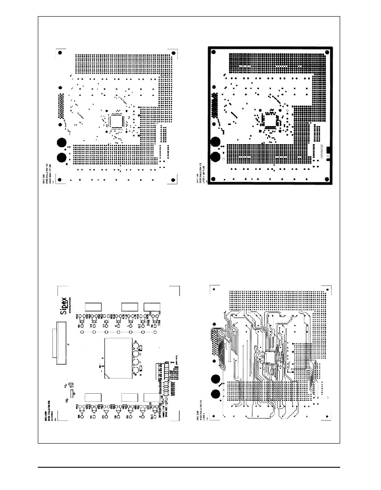
SP502/SP503 EVALUATION BOARD
The SP502/SP503 Evaluation Board (EB) Is
designed to offer as much flexibility to the user
as possible. Each board comes equipped with an
80-pin QFP Zero-Insertion Force socket to
allow for testing of multiple devices. The con-
trol lines and inputs and outputs of the device
can be controlled either manually or via a data
bus under software control. There is a 50-pin
connector to allow for easy connection to an
existing system via a ribbon cable. There are
also open areas on the PC board to add addi-
tional circuitry to support application-specific
requirements.
Manual Control
The SP502/SP503EB will support both the
SP502 or SP503 multi-mode serial transceiv-
ers. When used for the SP502, disregard all
notation on the board that is in [brackets] . The
SP502 has a half-duplex connection between
the RxT receiver and the TT driver. Due to this
internal connection, the RxT receiver inputs can
be accessed via the TT(a) and TT(b) pins. If the
user needs separate receiver input test pins,
jumpers JP1 and JP2 can be inserted to allow for
separate receiver inputs located at SCT(a) and
SCT(b). The corresponding TTL output for this
receiver is labeled as SCT. This test point is tied
to pin 79 of the SP502 or SP503. Pin 7 of the
evaluation board is connected to the DIP switch,
and is labeled as (SCTEN). When used with the
SP502, this pin should be switched to a low
state. When the evaluation board is used with
the SP503, pin 7 is a tri-state control pin for the
SCT receiver.
The transceiver I/O lines are brought out to test
pins arranged in the same configuration as shown
elsewhere in this data sheet. A top layer
silk-screen shows the drivers and receivers to
allow direct correlation to the data sheet. The
transmitter and receiver decode bits are tied
together and are brought out to a DIP switch for
manual control of both the driver and receiver
interface modes. Since the coding for the drivers
and receivers is identical, the bits have been tied
together. The DIP switch has 7 positions, four of
which are reserved for the TDEC/RDEC control
and the other three are used as tri-state control
pins. The labels that are in [brackets] apply only
to the SP503. If a logic one is asserted, the
corresponding red LED will be lit. If a zero is
asserted, the corresponding red LED will not
be lit.
Software Control
A 50-pin connector brings all the analog and
digital I/O lines, V
CC
, and GND to the edge of the
card. This can be wired to the user's existing
design via a ribbon cable. The pinout for the
connector is described in the following section.
When the evaluation board is operated under
software control, the DlP switch should be set
up so that all bits are LOW (all LEDs off). This
will tie 20k
pulldown resistors from the inputs
to ground and let the external system control the
state of the control inputs.
Power and Ground Requirements
The evaluation board layout has been optimized
for performance by using basic analog circuit
techniques, The four charge-pump capacitors
must be 22
µF (16V) and be placed as close to the
unit as possible; tantalum capacitors are sug-
gested. The decoupling capacitor must be a
minimum of 1
µF; depending upon the operating
environment, 10
µF should be enough for worst
case situations. The ground plane for the part
must be solid, extending completely under the
package. The power supplies for the device
should be as accurate as possible; for rated
performance
±5% is necessary. The power sup-
ply current will vary depending upon the se-
lected mode, the amount of loading and the data
rate. As a maximum, the user should reserve
200mA for I
CC
. The worst-case operating mode
is RS-485 under full load of six (6) drivers
supplying 1.6V to 54
loads. The power and
ground inputs can be supplied through either the
banana jacks on the evaluation board (Red = V
CC
= +5V
±5%; Black = GND) or through the con-
nector.
For reference, the 80-pin QFP Socket is a
TESCO part number FPQ-80-65-09A. The
50-pin connector is an AMP part number
749075-5.

21
Date: 7/29/04
SP503 Multiprotocol Transceiver
© Copyright 2004 Sipex Corporation
Figure 13. SP502/503 Evaluation Board Schematic
Date: 7/29/04
SP503 Multiprotocol Transceiver
© Copyright 2004 Sipex Corporation
22
Figure 14a. Evaluation Board -- Top Layers

23
Date: 7/29/04
SP503 Multiprotocol Transceiver
© Copyright 2004 Sipex Corporation
Figure 14b. Evaluation Board -- Bottom Layers

Date: 7/29/04
SP503 Multiprotocol Transceiver
© Copyright 2004 Sipex Corporation
24
Figure 15. External Transient Suppressors

25
Date: 7/29/04
SP503 Multiprotocol Transceiver
© Copyright 2004 Sipex Corporation
EDGE
DUT PIN
CONNECTOR
DESCRIPTIONS
01
TxD (pin 14) ≠TTL Input ≠ Transmit
data; source for SD(a) and SD(b) out-
puts.
02
DTR (pin 13) ≠ TTL Input ≠ Data
terminal ready: source for TR(a) and
TR(b) outputs.
03
ST/TT (pin 6) ≠TTL Input ≠ ST/TT
select pin; enables ST drivers and dis-
ables TT drivers when high. Disables
ST drivers and enables TT drivers when
low.
04
DEC
3
/RDEC
3
(pin 5) ≠ TTL Input ≠
Transmitter/Receiver decode register.
05
TDEC
2
/RDEC
2
(pin 4) ≠ TTL Input ≠
Transmitter/Receiver decode register.
06
TDEC
1
/RDEC
1
(pin 3) ≠ TTL Input ≠
Transmitter/Receiver decode register.
07
TDEC
0
/RDEC
0
(pin 2) ≠ TTL Input ≠
Transmitter/Receiver decode register.
08
RxD (pin 1 ) ≠ TTL Output ≠ Receive
data; sourced from RD(a) and RD)b)
inputs.
09
CTS (pin 80) ≠ TTL Output ≠ Clear to
send; sourced from CS(a) and CS(b)
inputs.
10
RxT (pin 79) ≠ TTL Output ≠ RxT;
sourced from TT(a), TT(b) inputs.
11
DSR (pin 78) ≠ TTL Output ≠ Data set
ready; sourced from DM(a) and DM(b)
inputs.
12
RD(b) (pin 71) ≠ Analog In ≠ Receive
data, non≠inverted; source for RxD.
EDGE
DUT PIN
CONNECTOR
DESCRIPTIONS
13
RD(a) (pin 70) ≠ Analog In ≠ Receive
data, inverted: source for RxD.
14
DM(b) (pin 69) ≠ Analog In ≠ Data
mode, non≠inverted; source for DSR.
l5
DM(a) (pin 68) ≠ Analog In ≠ Data
mode, inverted; source for DSR.
16
CS(b) (pin 67) ≠ Analog In ≠ Clear to
send; non≠inverted; source for CTS.
17
CS(a) (pin 66) ≠ Analog In ≠ Clear to
send, inverted; source for CTS.
18
TT(b) (pin 65) ≠ Analog Out ≠
Terminal timing, non≠inverted:
sourced from TxC input.
19
TT(a) (pin 63) ≠ Analog Out ≠
Terminal timing; inverted: sourced
from TxC input.
20
TR(a) (pin 58) ≠ Analog Out ≠ Termi-
nal ready, inverted; sourced from DTR.
21
TR(b) (pin 56) ≠ Analog Out ≠ Termi-
nal ready; non≠inverted; sourced from
DTR.
22
SD(a) (pin 61) ≠ Analog Out ≠ Send
data, inverted; sourced from TxD.
23
SD(b) (pin 59) ≠ Analog Out ≠ Send
data; non≠inverted; sourced from TxD.
24
RS(a) (pin 54) ≠ Analog Out ≠ Ready to
send; inverted; sourced from RTS.
25
RS(b) (pin 52) ≠ Analog Out ≠ Ready
to send, non≠inverted; sourced from
RTS.
1
26
2
27
3
28
4
29
5
30
6
31
7
32
8
33
9
34
10
35
11
36
12
37
13
38
14
39
15
40
16
41
17
42
18
43
19
44
20
45
21
46
22
47
23
48
24
49
25
50
Date: 7/29/04
SP503 Multiprotocol Transceiver
© Copyright 2004 Sipex Corporation
26
EDGE
DUT PIN
CONNECTOR
DESCRIPTIONS
26
ST (pin 22) ≠ TTL Input ≠ Send Tim-
ing; source for ST(a) and ST(b) out-
puts. SP503 only.
27
STEN (pin 23) ≠ TTL Input -- Driver
enable control pin; active low. SP503
only,
28
SCT(a) (pin 76) ≠ Analog Input ≠ In-
verting; input for SCT receiver; SP503
only.
29
SCT(b) (pin 77) ≠ Analog Input ≠ Non≠
inverting; input for SCT receiver.
SP503 only.
30
V
CC
-- +5V for all circuitry.
31
GND -- signal and power ground.
32 LL(a) (pin 51) ≠ Analog Out ≠ Local
loopback, inverted; sourced from LL.
33
LL(b) (pin 49) ≠ Analog Out ≠ Local
loopback, non≠inverted sourced from
LL.
34
RL(a) (pin 47) ≠ Analog Out ≠ Remote
loopback; inverted; sourced from RL.
35
RL(b) (pin 45) ≠ Analog Out ≠ Remote
loopback; non≠inverted; sourced from
RL.
36
ST(b) (pin 44) ≠ Analog Out ≠ Send
timing, non≠inverted; sourced from
TxC.
37
ST(a) (pin 42) ≠ Analog Output ≠Send
timing, inverted; sourced from TxC.
38
IC(b) (pin 40) ≠ Analog In ≠ Incoming
call; non≠inverted; source for Rl.
EDGE
DUT PIN
CONNECTOR
DESCRIPTIONS
39
IC(a) (pin 39) ≠ Analog In ≠ Incoming
call; inverted; source for Rl.
40
RT(b) (pin 38) ≠ Analog In ≠ Receive
timing, non≠inverted; source for RxC.
41
RT(a) (pin 37) ≠ Analog In ≠ Receive
timing; inverted; source from RxC.
42
RR(b) (pin 36) ≠ Analog In ≠ Receiver
ready; non≠inverted; source for DCD.
43
RR(a) (pin 35) ≠ Analog In ≠ Receiver
ready; inverted; source for DCD.
44
LL (pin 24) ≠ TTL Input ≠ Local
loopback; source for LL(a) and LL(b)
outputs.
45
Rl (pin 21) ≠ TTL Output ≠ Ring
indicator; sourced from IC(a) and IC(b)
inputs.
46
RxC (pin 20) ≠ TTL Output ≠ Receive
clock; sourced from RT(a) and RT(b)
inputs.
47
DCD (pin 19) ≠ TTL Output ≠ Data
carrier detect; sourced from RR(a) and
RR(b) inputs.
48
RL (pin 17) ≠ Analog Out ≠ Remote
loopback; source for RL(a) and RL(b)
outputs.
49
RTS (pin 16) ≠ TTL Input ≠ Ready to
send; source for RS(a) and RS(b) out-
puts.
50
TxC (pin 15) ≠ TTL Input ≠ Transmit
clock; source for TT(A) and TT(B)
outputs.
1
26
2
27
3
28
4
29
5
30
6
31
7
32
8
33
9
34
10
35
11
36
12
37
13
38
14
39
15
40
16
41
17
42
18
43
19
44
20
45
21
46
22
47
23
48
24
49
25
50

27
Date: 7/29/04
SP503 Multiprotocol Transceiver
© Copyright 2004 Sipex Corporation
PACKAGE: 80 PIN MQFP
80 PIN MQFP (MS-022 BC)
b
e
Seating
Plane
A1
A
A
L1
5∞-16∞
0∞ MIN.
0∞≠7∞
5∞-16∞
L
A2
0.30" RAD. TYP.
0.20" RAD. TYP.
c
PIN 1
E1
D1
D
CL
E
CL
D2
E2
DIMENSIONS
Minimum/Maximum
(mm)
SYMBOL
A
A1
A2
b
D
D1
D2
E
E1
E2
e
N
80≠PIN MQFP
JEDEC MS-22
(BEC) Variation
MIN
NOM
MAX
2.45
0.00
0.25
1.80
2.00
2.20
0.22
0.40
17.20 BSC
14.00 BSC
12.35 REF
17.20 BSC
14.00 BSC
12.35 REF
0.65 BSC
80
COMMON DIMENTIONS
SYMBL MIN
NOM
MAX
c
0.11
23.00
L
0.73
0.88
1.03
L1
1.60 BASIC

Date: 7/29/04
SP503 Multiprotocol Transceiver
© Copyright 2004 Sipex Corporation
28
PACKAGE: 80 PIN LQFP
R2
R1
b
e
Seating
Plane
A1
A
A
PIN 1
E1
D1
D
CL
CL
E
L
¯2
¯1
¯
¯3
80 PIN LQFP
A1
L1
1.60
0.15
0.75
MAX
1.45
0.38
DIMENSIONS
Minimum/Maximum
(mm)
SYMBOL
A
A1
A2
b
80≠PIN LQFP
JEDEC MS-026
(BEC) Variation
1.40
0.05
16.00 BSC
14.00 BSC
16.00 BSC
14.00 BSC
0.45
MIN
NOM
1.35
1.40
0.22
0.32
D
D1
E
E1
L
e
0.65 BSC
L1
1.00 REF
¯
0∫ 3.5∫ 7∫
¯1
0∫ - -
¯2
11∫ 12∫ 13∫
¯3
11∫ 12∫ 13∫
R1
0.08 - -
R2
0.08 - 0.20

29
Date: 7/29/04
SP503 Multiprotocol Transceiver
© Copyright 2004 Sipex Corporation
ORDERING INFORMATION
Part Number Top Mark
Temperature Range
Package Types
SP503CF ............. SP503CFYYWW......0∞C to +70∞C ............................ 80≠pin JEDEC (MS-022 BC) MQFP
SP503EF.............SP503EFYYWW......-40∞C to +85∞C .......................... 80≠pin JEDEC (MS-022 BC) MQFP
SP503EM.............SP503EMYYWW......-40∞C to +85∞C .......................... 80≠pin JEDEC (MS-022 BC) LQFP
Corporation
ANALOG EXCELLENCE
Sipex Corporation reserves the right to make changes to any products described herein. Sipex does not assume any liability arising out of the
application or use of any product or circuit described hereing; neither does it convey any license under its patent rights nor the rights of others.
Sipex Corporation
Headquarters and
Sales Office
233 South Hillview Drive
Milpitas, CA 95035
TEL: (408) 934-7500
FAX: (408) 935-7600
DATE
REVISION
DESCRIPTION
1/27/04
A
Implemented tracking revision.
5/6/04
B
Added Top Mark to ordering information.
7/29/04
C
Included LQFP package option.
REVISION HISTORY
Available in lead free packaging. To order add "-L" suffix to part number.
Example: SP503EF = standard; SP503EF-L = lead free