 | –≠–ª–µ–∫—Ç—Ä–æ–Ω–Ω—ã–π –∫–æ–º–ø–æ–Ω–µ–Ω—Ç: SP503EB | –°–∫–∞—á–∞—Ç—å:  PDF PDF  ZIP ZIP |
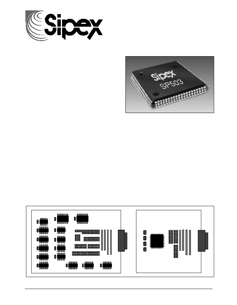
SP503AN
SP503 Application Note
© Copyright 2000 Sipex Corporation
1
Due to its flexibility and programmability,
the SP503 has been finding its way into
many new networking products. The SP503
offers an excellent replacement for discrete
solutions on X.25 implementations for frame
relay systems, multi-protocol routers and
other WAN products where many designs
run various modes such as RS-232,
RS-422, V.35 or V.36.
For RS-232, the older bipolar 1488 and
1489 parts, or even the newer MAX230 or
SP230 series have traditionally been used.
For RS-422 or RS-485, the 26LS31,
26LS32, 3488, and 3489 have been seen in
many designs. These parts have been also
used for V.35 but with external termination
resistors. For a typical design, four RS-232
chips would be used for a complete
RS-232 port, four RS-422 chips for an
RS-422 port and four chips for V.35 with an
external resistor network. Port programma-
bility would require relays or switches so
that software lines can control whether
RS-232 is active or RS-422 is active. The
relays increase board capacity as well as
cost to the design.
The SP503 solves board space and cost
problems by offering a single packaged part
that supports various protocols and also
offers software programmability to the port.
s
DTE and DCE configurations with
the SP503
s
Connecting the SP503 to a DB-25
connector in DTE and DCE modes
s
Implementing V.35 with the SP503
s
Creating extra single-ended and
differential channels with the SP503
using the SP310A and SP485
s
Using external supplies with the SP503
SP503
Application Note
Typical discrete solution vs. the SP503
Æ

SP503AN
SP503 Application Note
© Copyright 2000 Sipex Corporation
2
DTE and DCE configurations
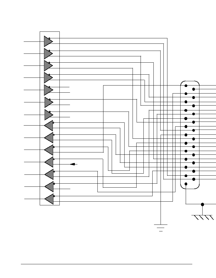
with the SP503
The SP503 has designated signals such as "Trans-
mit Data", "Clear-to-Send", etc.which design-
ers can easily allocate the appropriate SP503
transceivers for the corresponding signals. The
data signals specified in the EIA standards and
CCITT are referenced in the SP503 datasheet as
DTE. Some customers have wondered if they
can use the SP503 for DCE applications.
Although it can be confusing at first glance, the
DCE implementation is the mirror image of the
DTE side. For the DTE, TxD is a driver which
drives the data to RxD, a receiver, on the DCE
side. TxC or TT is a driver on the DTE side
which drives the clock signal to the RxC re-
ceiver on the DCE side.
The next three pages illustrate the CCITT signal
allocations from the SP503 in either DTE or
DCE to the DB-25 connector. As shown, it is
possible to use a DB-25 connector for the vari-
ous protocols offered by the SP503.
DB-25 Connector Pin Assignments for Various Protocols
DB-25 Pin #
RS-232
EIA-530
RS-449
RS-422
V.35
V.36
1
shield
shield
shield
shield
CCITT# 101 CCITT# 101
2
TxD
TxD(A)
SD(A)
T(A)
103(A)
103(A)
3
RxD
RxD(A)
RD(A)
R(A)
104(A)
104(A)
4
RTS
RTS(A)
RS(A)
C(A)
105
105(A)
5
CTS
CTS(A)
CS(A)
≠
106
106(A)
6
DSR
DSR(A)
DM(A)
≠
107
107(A)
7
Signal GND
Signal GND
Signal GND
Signal GND
102
102
8
DCD
RLSD(A)
RR(A)
I(A)
109
109(A)
9
≠
RxC(B)
RT(B)
≠
115(B)
115(B)
10
≠
RLSD(B)
RR(B)
I(B)`
≠
109(B)
11
≠
TxC(B-DTE)
TT(B)
≠
113(B)
113(B)
12
DCD (2nd)
TxCC(B-DCE)
ST(B)
S(B)
114(B)
114(B)
13
CTS (2nd)
CTS(B)
CS(B)
≠
≠
106(B)
14
TxD (2nd)
TxD(B)
SD(B)
T(B)
103(B)
103(B)
15
TxCC (DCE) TxCC(A-DCE)
ST(A)
S(A)
114(B)
114(B)
16
RxD (2nd)
RxD(B)
RD(B)
R(B)
104(B)
104(B)
17
RxC
RxC(A)
RT(A)
≠
115(A)
115(A)
18
LL
LL
LL
≠
≠
141
19
RTS (2nd)
RTS(B)
RS(B)
C(B)
≠
105(B)
20
DTR
DTR(A)
TR(A)
≠
≠
≠
21
RL
RL
RL
≠
≠
140
22
RI
DSR(B)
DM(B)
≠
≠
107(B)
23
SRS
DTR(B)
TR(B)
≠
≠
≠
24
TxC (DTE)
TxC(A-DTE)
TT(A)
≠
113(A)
113(A)

SP503AN
SP503 Application Note
© Copyright 2000 Sipex Corporation
3
DTE-DCE flexibility with the SP503 on a DB-25 serial port
DB-25
Connector
TxD
TxC
DTR
RTS
RxD
RxC
CTS
DCD
TxD
TxC
DTR
RTS
RxD
RxC
CTS
DCD
RDEC0
RDEC1
RDEC2
RDEC3
TDEC0
TDEC1
TDEC2
TDEC3
2 3
4
5 12 11 10 9
2 3 4 5 12 11 10 9
14
15
13
16
1
20
80
19
DSR
RI
SCT
LL
RL
ST
78
21
79
24
17
22
Quad 2:1 Mux
1Y
2Y
3Y
4Y
1A
1B
2A
2B
3A
3B
4A
4B
SEL
"0" = DTE
"1" = DCE
SCC
61
SD(A)
SD(B)
TT(A)
TT(B)
TR(A)
TR(B)
RS(A)
RS(B)
RT(A)
RT(B)
RD(A)
RD(B)
CS(A)
CS(B)
RR(A)
RR(B)
DM(A)
DM(B)
SCT(A)
SCT(B)
IC(A)
IC(B)
LL(A)
LL(B)
ST(A)
ST(B)
SP503
DTE
Config.
SP503
DCE
Config.
59
63
65
58
56
54
52
70
71
37
38
66
67
35
36
68
69
76
77
39
40
51
49
42
44
61
59
63
65
58
56
54
52
70
71
37
38
66
67
35
36
68
69
76
77
39
40
51
49
42
44
47
RL(A)
47
3
16
17
9
6
22
5
13
2
14
24
11
4
19
18
20
23
21
8
15
12
22
10
TxD
TxC
DTR
RTS
RxD
RxC
CTS
DCD
14
15
13
16
1
20
80
19
DSR
RI
SCT
LL
RL
ST
78
21
79
24
17
22
SD(A)
SD(B)
TT(A)
TT(B)
TR(A)
TR(B)
RS(A)
RS(B)
RT(A)
RT(B)
RD(A)
RD(B)
CS(A)
CS(B)
RR(A)
RR(B)
DM(A)
DM(B)
SCT(A)
SCT(B)
IC(A)
IC(B)
LL(A)
ST(A)
ST(B)
RL(A)
LL(B)
7
1
SP503AN
SP503 Application Note
© Copyright 2000 Sipex Corporation
4
Driver / Receiver Connections to a DB-25 Connector
DTE Mode
Male
Connector
1
14
13
25
TxD
Drivers
Receivers
DTR
RTS
14
13
16
15
TxC
SP503CF
RxD
RxC
CTS
DSR
DCD
1
20
80
78
19
RI
21
SCT
79
17
RL
24
LL
ST
22
to pin 22 for non-RS-232
RI used for RS-232 only
61
59
58
56
63
42
54
52
65
44
47
51
45
49
70
71
37
38
66
67
68
69
35
36
40
77
39
76

SP503AN
SP503 Application Note
© Copyright 2000 Sipex Corporation
5
Driver / Receiver Connections to a DB-25 Connector
DCE Mode
TxD Drivers
Receivers
DTR
RTS
14
13
16
15
TxC
SP503CF
RxD
RxC
CTS
DSR
DCD
1
20
80
78
19
RI
21
SCT
79
17
RL
24
LL
ST
22
Female
Connector
1
14
13
25
to pin 22 for non-RS-232
TxD(A)
TxD(B)
TxC(A)
TxC(B)
RTS(A)
RTS(B)
DTR(A)
DTR(B)
LL
RL
RxD(A)
RxD(B)
DSR(A)
CTS(A)
CTS(B)
RxC(A)
RxC(B)
SCT(A)
SCT(B)
RI
DCD(A)
DCD(B)*
49
51
45
47
44
42
65
63
52
54
58
59
61
39
35
69
68
67
37
70
71
38
66
36
40
76
77
56
* The non-inverting LL driver output is not a
valid driver output for RS-449 and EIA-530.
SP503AN
SP503 Application Note
© Copyright 2000 Sipex Corporation
6
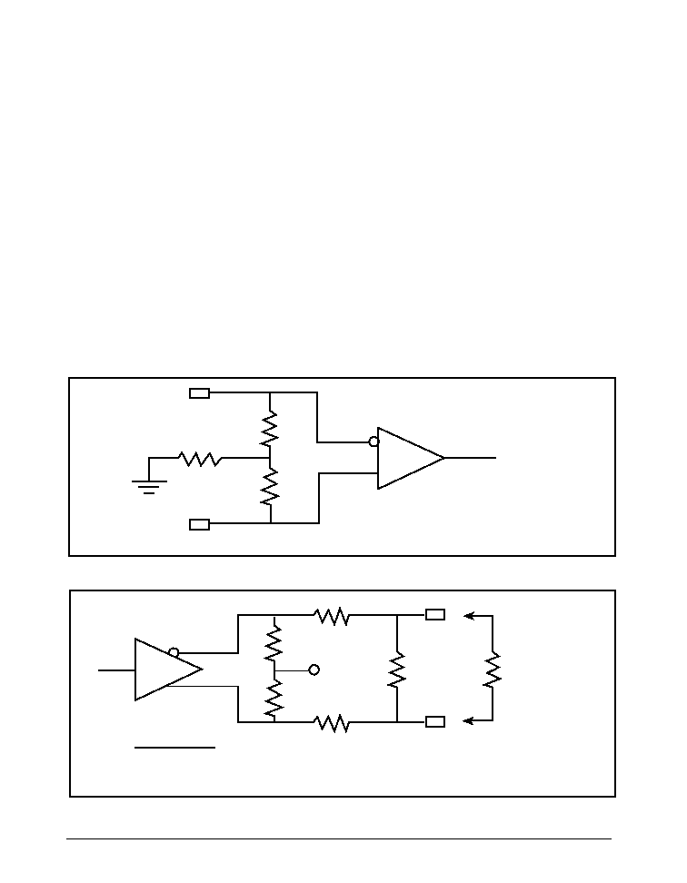
SP503 V.35 External Termination
Resistors
V.35 implementation requires external resistors
to be connected to the driver outputs and re-
ceiver inputs. The resistors are needed for
reducing signal levels and maintaining input
and output impedance levels that conform to
CCITT Recommendation V.35. The drawings
below offer both receiver input termination and
driver output termination configurations that
will comply to V.35.
As you may know, the termination resistors are
for V.35 mode only and have to be disconnected
when another mode is programmed. There are
a few ways to connect and disconnect the net-
work. One method is to add a daughter-card
option slot onto the main printed circuit board
where the SP503 is mounted. This allows the
user to add a mini-PC card that contains the V.35
network to be connected to the driver outputs
and receiver inputs. Another method is to
implant the V.35 network into a cable if the user
requires conversion cables to switch from one
protocol to another. For example, if the serial
port has a DB-25 connector and requires an
ISO-2593 connector for V.35; a DB-25 to
ISO-2593 conversion cable containing the V.35
network is connected to the port.
Of course this method will not allow program-
mability to the serial port if the user wants to run
various protocols to that port. To actively switch
protocols by software control, you can use ana-
log switches or relays. Sipex recommends us-
ing low-ON resistance analog switches, such as
Siliconix DG643
©
analog switches for the driver
outputs, and solid-state relays such as the AT&T
LH1514
©
for the receiver inputs. See opposite
page for an example of the SP503 V.35 configu-
ration. For other termination networks, please
consult the factory.
50
50
120
A
B
Z
SOURCE
= 97
Z
SC
= 148
[90
to 110
]
[135
to 165
]
232
232
200
200
107
A
B
100
LOAD
-5V
±
5%
Z
SOURCE
= 96
Z
SC
= 154
[50
to 150
]
[135
to 165
]
V
D
= 0.55V
V
DC_OFF
= 0.0V
[+0.44V to +0.66V]
[-0.6V to +0.6V]
Typical values
V.35 Receiver Input Termination Resistor Network
V.35 Driver Output Termination Resistor Network

SP503AN
SP503 Application Note
© Copyright 2000 Sipex Corporation
7
SP503 Switching Configuration for V.35 Implementations
∑ Switches are Siliconix DG643DY analog switches.
∑ Solid-State Relays are AT&T, LH1514.
∑ Resistors are 1/8W, 1% tolerance.
∑ External Supplies necessary are: V
cc
= +5V, V+ = +12V (for V+ on the DG643DY) and V
n
= -5V.
Receivers
TxD
Drivers
DTR
RTS
14
13
16
15
TxC
SP503CF
RxD
RxC
CTS
DSR
DCD
1
20
80
78
19
RI
21
SCT
79
17
RL
24
LL
ST
22
V+
V-
+5V
Driver Outputs & Receiver Inputs
are in DTE mode.
to pin 12 of the 74LS11
to pin 12 of the 74LS11
to pin 12 of the 74LS11
74LS11
74LS11
74LS11 (3-Input AND Gate)
RxC (115)
A
B
RxD (104)
A
B
A
B
A
B
TxD (103)
A
B
TT (113)
TxCC (114)
A
B
to pin 6 of the 74LS11
74LS11
LH1514
74LS11
1
3
LH1514
7
5
1
LH1514
7
5
+12V
50
50
120
3
1
8
6
50
50
120
8
6
3
50
50
120
8
2
15
9
12
5
3
7
10 14
4
6
13
11
8
2
15
9
12
5
7
3
10
14
4
6
11
13
1
16
1
16
V+
V-
V+
DG643
DG643
200
200
232
232
-5V
107
V-
to V-
+12V
8
2
15
9
12
5
3
7
10 14
4
6
13
11
8
2
15
9
12
5
7
3
10
14
4
6
11
13
1
16
1
16
V+
V-
V+
DG643
DG643
+12V
200
200
232
232
-5V
107
V-
8
2
15
9
12
5
3
7
10 14
4
6
13
11
8
2
15
9
12
5
7
3
10
14
4
6
11
13
1
16
1
16
V+
V-
V+
DG643
DG643
+12V
+12V
200
200
232
232
-5V
107
+5V
16
1
13
2
12
1/4
74LS11
8
+5V
16
3
5
4
6
8
RDEC1 & TDEC1
RDEC2 & TDEC2
RDEC3 & TDEC3
(pins 3 & 11)
(pins 4 & 10)
(pins 5 & 9)
to pin 6 of the 74LS11
74LS11
8
6
7
5
1/4
74LS11

SP503AN
SP503 Application Note
© Copyright 2000 Sipex Corporation
8
Typical Applications Questions
on the SP503
Can the SP503 be used with external power
supplies? If so, is there a power-up sequence?
The internal charge pump can be bypassed
through external supplies to V
DD
and V
SS
. The
external voltage should be +10V for V
DD
and
-10V for V
SS
. The tolerance is
±
5%. The
absolute minimum limit for the external supplies
is
±
7V and the absolute maximum limit is
±
10.5V.
The SP503 does require a power-up sequence of
+10V, +5V, -10V for proper operation. Addi-
tional external circuitry will be required for the
correct sequencing. Consult factory for details.
What is the maximum input voltage applied to
the receiver input without damaging the SP503?
The receiver inputs can tolerate up to
±
16V in
any protocol without latching up the device.
Since RS-232 ranges from
±
5V to
±
15V; the
SP503 is well within the accepted range. It may
be worthwhile to include 15V clamping diodes
or transient voltage suppressors so that the re-
ceiver input will be held below
±
15V.
What is the maximum short-circuit voltage that
can be applied to a SP503 driver output?
The driver outputs can be shorted up to
±
16.0V
without causing damage to the driver. Between
the
±
16V range, the SP503 adheres to the RS-
232 short circuit current limit of 100mA and to
the RS-422/RS-423 limit at 150mA. Again,
transient voltage suppressors or clamping diodes
will protect the SP503 if exceeding the
±
16V
range is possible.
What is the state of the SP503 drivers and
receivers when the device is addressed with
0000?
The SP503 drivers are in a high impedance(over
1M
) tri-state condition when "0000" is ad-
dressed. The receivers are not tri-stated and the
outputs are undefined. This means that they
could be floating to either a high or low level
depending on the previous state of the receiver
input prior to the 0000 addressing change. The
receiver input impedance is at 15k
for "0000".
Can the SP503 be programmed for 7 drivers and
7 receivers in RS-423 mode?
The SP503 can be switched to RS-423 mode by
programming TDEC
3
, TDEC
2
, TDEC
1
, TDEC
0
to "1000" for the drivers and RDEC
X
to "1000"
for the receivers. However, external supplies
must be used in order to drive RS-423. The
internal charge pump can only support up to
three RS-423 drivers and three RS-423
receivers.
What is the power dissipation in the SP503 and
in which mode does it consume the most power?
The SP503 dissipates approximately 400mW to
1.4W depending on the protocol. RS-485 mode
consumes the most power at 1.4W. For worst
case power dissipation, all seven drivers were
driven with a TTL signal and the outputs were
looped back into the receiver inputs to generate
a TTL output. All drivers and receivers were
active.
MODE
P
D
RS-232
0.418W
RS-422
0.970W
RS-485
1.382W
RS-449
0.959W
EIA-530
0.959W
V.35
1.055W
What is the state of the SP503 drivers and
receivers when the device is addressed with
1111?
The address for "1111" is not used in the SP503.
If the SP503 is programmed for "1111", the
drivers are approximately 1.0V and at a high
impedance (approx. 9M
). The receivers are
not tri-stated and the outputs are undefined. All
receiver inputs are at 15k
input impedance.
The SP503 can receive a "1111" address while
V
CC
is off. The supply current is approximately
50mA (V
CC
= +5V) while the address is at
"1111".
In the RS-232 signal assignments for the DB-25
connector, where does the SP503 account for
Test Mode (TM) ?
For most RS-232 applications, the signals com-
monly used are TxD, TxC, RxD, RxC, RTS,
CTS, DSR, SG, DCD, DTR and Frame Ground.

SP503AN
SP503 Application Note
© Copyright 2000 Sipex Corporation
9
In DTE mode; TxD, TxC, RTS, DTR are the
drivers and RxD, RxC, CTS, DSR, DCD are the
receivers. Since there are seven drivers and
seven receivers in the SP503, the designer can
easily use the SP503 for the above signals. Other
RS-232 applications will support diagnostic func-
tions such as LL (driver), RL (driver), and TM
(receiver) which may or may not require extra
transceivers depending if other signals are not
used. Since Test Mode (TM) is a receiver for
DTE designs, the Ring Indicator (RI) receiver in
the SP503 (pin 21) can be used for TM if RI is not
used. If all the available drivers and receivers are
used in the SP503, then another RS-232 trans-
ceiver can be added. See page 230 and 231 for
suggestions on adding Sipex's RS-232 and
RS-485 transceivers.
Are the Schottky diodes used from Vcc to Vss
and from Vdd to C2- in the SP502 necessary for
the SP503?
Sipex has incorporated the Schottky diodes
(needed with the SP502) into the SP503 in order
to protect against potential start up problems due
to fast rate of rise on V
CC
(
1V/
µ
s) and overvolt-
age to the TTL inputs. However, a negative
voltage (V
in
-5V) applied to the receiver inputs
while the SP503 is powered off will cause start-
up problems to the charge pump. In order to
guard against this condition, an external Schottky
diode should be placed from V
CC
to V
DD
to
minimize V
CC
current injection into the IC sub-
strate and allow the charge pump to operate
properly. See page 203 Figure 6 - Typical
Operating Circuit, for diode connection
schematic.
Can the SP503 be configured for V.36?
CCITT Recommendation V.36 is similar to RS-
449 where certain signals are RS-422 signals and
others are RS-423. Depending on different ap-
plications; "Transmit Data", "Terminal Timing",
"Request-to-Send", "Data Terminal Ready",
"Receive Data", "Transmit Clock", "Receive
Clock", "Clear-to-Send", "Data Carrier Detect",
and "DataSet Ready" are specified as Category 1
Circuits where the protocol is RS-422 for rates
over 20kbps. All other circuits are Category 2
Circuits which are specified as RS-423 circuits.
Depending on particular signals, the SP503 can
be easily used for V.36.
When the two drivers, ST and TT, are in tri-state
mode, what will the driver outputs tolerate for
maximum short circuit voltages? And the re-
ceiver, SCT, input?
The driver outputs will tolerate up to
±
16.0V
without any damage to the circuit regardless of
whether or not ST and TT are in tri-state mode.
The tri-state circuitry does not affect the short
circuit protection on the driver outputs. The SCT
receiver input will tolerate up to
±
16.0V without
any damage to the input structure regardless of
whether or not SCT is in tri-state mode.
What does Sipex recommend for transient volt-
age suppression techniques for the SP503?
For our evaluation boards, Sipex uses transient
voltage suppressor ICs from ProTek Devices,
model numbers LCA05C to LCA15C. The two
digits in the part number pertain to the rated
stand-off voltage, V
WM
, which is the maximum
working DC voltage applied to the device. These
TVS devices are especially designed for serial
data communications because of their low ca-
pacitance and low impedance. However, please
be aware that V
WM
values below the specified
input range of the transceiver will affect the input
impedance. For example, it would be fine to use
a 5V V
WM
value for RS-422 but for RS-232, the
receiver input voltage range is
±
15V where lower
V
WM
voltages will drive the impedance to ground.
Another recommended manufacturer is AVX
Corporation TransGuard series of TVS compo-
nents. AVX offers a variety of surface mount
back-to-back diodes.
ProTek Devices ∑ P.O. Box 3129 ∑ Tempe, AZ. 85280
∑ 602-431-8101
AVX Corporation ∑ Myrtle Beach, SC ∑ 803-448-9411
The drawing on page 232 shows the SP503
configured with the ProTek SM16LC15C TVS
devices to protect the drivers and receivers from
ESD and over-voltage.
Will the SP503 conform to the physical layer
testing specified by NET1/NET2 for X.21 and
X.25 systems?
Sipex initiated a component level test for NET1/
NET2 for V.28, V.10, V.11, V.35 protocols. The
SP503 passed all the physical layer testing re-
quirements prescribed by NET1/NET2. A full
test report can be furnished upon request.

SP503AN
SP503 Application Note
© Copyright 2000 Sipex Corporation
10
Creating extra RS-232 channels using the SP310A
22
µ
F
22
µ
F
22
µ
F
25
27
26
30
28
31
32
1N5819
V
CC
V
DD
C1-
C2- V
SS
C1+
C2+
22
µ
F
61
1
7
2
14
59
+5V
SP503CF
Drivers
TxD
14
58
20
23
56
DTR
13
54
4
19
52
RTS
16
63
24
11
65
TxC
15
42
44
ST
22
47
21
45
RL
17
51
18
49
LL
24
70
3
16
71
RxD
1
37
17
9
38
RxC
20
66
5
13
67
CTS
80
68
6
69
DSR
78
35
8
10
36
DCD
19
39
22
40
RI
21
76
15
12
77
SCT
79
Receivers
+5V
17
V+
SP310ACT
3
RDEC
1
RDEC
1
DB-25 connector in
DTE configuration.
25
7
31
V
CC
V
DD
C1-
C2- V
SS
C1+
C2+
V
CC
C1-
C2-
C1+
C2+
ON/OFF
V-
3
2
4 5
6
18
12
11
TM
13
10
9
14
8
15
0.1
µ
F
0.1
µ
F
0.1
µ
F
0.1
µ
F
(Pin 3 of
the SP503)

SP503AN
SP503 Application Note
© Copyright 2000 Sipex Corporation
11
Creating extra differential channels using the SP485
22
µ
F
22
µ
F
22
µ
F
25
27
26
30
28
31
32
1N5819
V
CC
V
DD
C1-
C2- V
SS
C1+
C2+
22
µ
F
61
1
7
2
14
59
+5V
SP503CF
Drivers
TxD
14
58
20
23
56
DTR
13
54
4
19
52
RTS
16
63
24
11
65
TxC
15
42
44
ST
22
47
21
45
RL
17
51
18
49
LL
24
70
3
16
71
RxD
1
37
17
9
38
RxC
20
66
5
13
67
CTS
80
68
6
69
DSR
78
35
8
10
36
DCD
19
39
22
40
RI
21
76
15
12
77
SCT
79
Receivers
+5V
8
6
7
V
CC
1
µ
F
SP485
4
10
TDEC
2
TDEC
2
DB-25 connector in
DTE configuration.
25
3
RDEC
1
1
2
(pin 3 of the SP503)
DI
DE
RO
RE
5
B
A

SP503AN
SP503 Application Note
© Copyright 2000 Sipex Corporation
12
Using Transient Voltage Suppressors with the SP503
22
µ
F
25
27 26 30
32
1N5819
V
CC
V
DD
C1-
C2-
V
SS
C1+
C2+
22
µ
F
SP503CF
Drivers
TxD
14
DTR
13
RTS
16
TxC
15
ST
22
RL
17
LL
24
RxD
1
RxC
20
CTS
80
DSR
78
DCD
19
RI
21
SCT
79
Receivers
* - Please note that the ProTek transient
voltage suppressors should also be con-
nected to the other SP503 drivers and re-
ceivers in the same configuration as shown
above.
28 31
22
µ
F
+5V
15
14
13 12
11 10
2
3
4
5
6
7
ProTek Devices
SM16LC15C
15
14
13 12
11 10
2
3
4
5
6
7
ProTek Devices
SM16LC15C

SP503AN
SP503 Application Note
© Copyright 2000 Sipex Corporation
13
ORDERING INFORMATION
Model
Temperature Range
Package Types
SP503CF ............................................... 0
∞
C to +70
∞
C .................................................................. 80≠pin QFP
SP503EB ....................................................................................................................SP503 Evaluation Board
Corporation
SIGNAL PROCESSING EXCELLENCE
Sipex Corporation reserves the right to make changes to any products described herein. Sipex does not assume any liability arising out of the
application or use of any product or circuit described hereing; neither does it convey any license under its patent rights nor the rights of others.
Sipex Corporation
Headquarters and
Sales Office
22 Linnell Circle
Billerica, MA 01821
TEL: (978) 667-8700
FAX: (978) 670-9001
e-mail: sales@sipex.com
Sales Office
233 South Hillview Drive
Milpitas, CA 95035
TEL: (408) 934-7500
FAX: (408) 935-7600