 | –≠–ª–µ–∫—Ç—Ä–æ–Ω–Ω—ã–π –∫–æ–º–ø–æ–Ω–µ–Ω—Ç: SP504CF | –°–∫–∞—á–∞—Ç—å:  PDF PDF  ZIP ZIP |

SP504AN
SP504 Application Note
© Copyright 2000 Sipex Corporation
1
Typical Environment Using Frame Relay and X.25 Systems
Multi-
Protocol
Router
Frame
Relay
Switch
X.25
Switch
FRAD
&
X.25
Switch
Workstations
Workstations
PCs
PCs
Mainframe
Mainframe
Mainframe
Workstations
Workstation
Workstation
PC
PC
PCs
2.1Mb/s
1.5Mb/s
Corporate Office
Engineering/Manufacturing
Remote Office
Branch Office
56kb/s
56/64kb/s
Frame
Relay
The introduction of our SP502 transceiver paved
the way for a new generation of multi-mode
transceivers that are being designed into next
generation networking products. The SP504
multi-mode transceiver is the latest member of
the family and offers: reduced external V.35
termination; V.36 & EIA-530A modes; and
receiver tri-state and fail-safe ability.
As with the SP502 and SP503, the SP504 can be
programmed via software to the different avail-
able physical protocols and is also drop-in com-
patible with its predecessors.
The versatility of the SP504 is ideal for multi-
protocol applications such as Frame Relay sys-
tems, X.25 routers/switches and multi-protocol
routers. These multi-protocol systems will usu-
ally contain multiple ports to accommodate the
different interfaces. The SP504 can support all
the ports through software and provide conve-
nient DTE or DCE functionality to the port. DTE
and DCE configuration is provided on the next
page and also in the SP504 data sheet.
The designer can evaluate the SP504 with
our SP504 Evaluation Board. This evaluation
board basically allows the user to access the
pins directly through probe points on the board.
The designer can also access the device by
software through the three serial port connec-
tors on the board. Details on the evaluation
board can be found in the SP504 data sheet.
SP504
Application Note
Æ

SP504AN
SP504 Application Note
© Copyright 2000 Sipex Corporation
2
SP504 - Overvoltage and ESD Protection Using Transzorbs
Although the SP504 is internally protected for ESD
and overvoltage, an external transient voltage sup-
pression circuit can be added to increase the level of
protection of the device. This may be desired for
greater ESD protection or clamping the input or out-
put voltages. The maximum driver output and re-
ceiver input voltages should not exceed
±
15V.
The SP504 configuration above uses ProTek Devices'
SM16LC15C TVS devices to protect the receiver in-
puts and the driver outputs since these pins are di-
rectly exposed to the connector and the outside world.
The V
wm
of the TVS can be as low as 5V and high as
15V to cover the RS-232 voltage levels. However,
the RS-232 3k
to 7k
input impedance will not
comply if the voltage levels exceed the clamping
voltage of the TVS.
ProTek Devices ∑ Tempe, AZ. ∑ 602-431-8101
22
µ
F
25
27
26 30
32
1N5819
V
CC
V
DD
C1-
C2-
V
SS
C1+
C2+
22
µ
F
SP504CF
Drivers
TxD
14
DTR
13
RTS
16
TxC
15
ST
22
RL
17
LL
24
RxD
1
RxC
20
CTS
80
DSR
78
DCD
19
RI
21
SCT
79
Receivers
* - Please note that the ProTek transient
voltage suppressors should also be con-
nected to the other SP504 drivers and re-
ceivers in the same configuration as shown
above.
28
31
22
µ
F
+5V
15
14 13
12
11 10
2
3
4
5
6
7
ProTek Devices
SM16LC15C
ProTek Devices
SM16LC15C
15
14 13
12
11 10
2
3
4
5
6
7

SP504AN
SP504 Application Note
© Copyright 2000 Sipex Corporation
3
SP503/504 - One Chip Half-Duplex Configuration
22
µ
F
22
µ
F
22
µ
F
25
27
26
30
28
31
32
1N5819
V
CC
V
DD
C1-
C2-
V
SS
C1+
C2+
22
µ
F
61
59
+5V
SP503CF or SP504CF
Drivers
TxD
14
58
56
DTR
13
54
52
RTS
16
63
65
TxC
15
42
44
ST
22
47
45
RL
17
51
49
LL
24
70
71
RxD
1
37
38
RxC
20
66
67
CTS
80
68
69
DSR
78
35
36
DCD
19
39
40
RI
21
76
77
SCT
79
Receivers
TDEC
3
10
µ
F
9
10
11
12
TDEC
0
TDEC
1
TDEC
2
9
10
11
12
RDEC
0
RDEC
1
RDEC
2
RDEC
3
TxD/RxD
DTR/DSR
RTS/CTS
TxC/RxC
ST/SCT
RL/RI
LL/DCD
Dr
iv
er Decoder
Receiv
er
Decoder
29, 34, 46, 50, 53, 57, 60, 64, 72, 75 GND

SP504AN
SP504 Application Note
© Copyright 2000 Sipex Corporation
4
SP504 - DTE/DCE Configuration
Many systems may require the serial port to be
configured as either a DTE or DCE. The SP504
is an ideal candidate for a space saving DTE/
DCE solution.
To perform this with the SP504, the driver out-
puts of the first SP504 are connected back into
the receiver inputs of the second SP504, and
vice versa. The common input/output lines can
be routed to the connector and be used as ei-
ther driver outputs or receiver inputs. Refer to
the following page for configuration details.
When the two SP504 devices are connected as
such, one device must be disabled while the
other is transmitting and receiving data. Dis-
abling one of the SP504 devices allows the
other to communicate over the serial bus. One
is dedicated to a DTE configuration to the se-
rial port and the other is a dedicated DCE de-
vice. Disabling the DTE device implies that
the serial port will be configured as a DCE, and
vice versa.
Disabling the SP504 drivers are important be-
cause a bus contention problem can occur if
two drivers are active at the same time. The
drivers of the nonactive SP504 must be tri-
stated by writing "0000" into the driver decoder
(TDEC
X
) lines when the I/O lines are used as
inputs into the receivers. The receivers do not
have to be tri-stated but should be configured
so that the receiver input impedance is rela-
tively high (
12k
) such as RS-422 or RS-485.
The receiver inputs will not affect the signals
on the driver outputs if the input impedance is
at least 12k
. If the RDEC
X
is configured with
"0000", the input impedance defaults to at least
12k
.
Please note that most of the V.35 termination
resistors are internal to the SP504. As such, the
driver output impedance during tri-state is
approximately 20k
. This should not affect or
degrade the incoming driver signal from the
other end. Refer to the waveform graphs in the
next few pages. The "DTE" waveforms cap-
ture the driver and receiver signals at the serial
port containing the two SP504 devices. The
"DCE" waveforms are measured in the SP504
at the other end. For example, the TxD driver
output on the DCE side corresponds to the RxD
receiver on the DTE side (side containing two
SP504 devices). Similarly, the TxC driver out-
put on the DTE side should be the same as the
RxC receiver input on the DCE side.
Even though the signal is not degraded, the
lower impedance basically adds the driver out-
put impedance (20k
) and the receiver input
impedance in parallel. When the active SP504
is configured to RS-232 mode, the typical re-
ceiver input impedance is 5k
which will yield
4k
. When in the other modes except V.35,
the typical input impedance is 15k
which
yields 7.5k
when the receivers are configured
in differential mode (i.e. RS-422, RS-449, V.36,
etc.) which is still greater than the 4k
mini-
mum requirement for RS-422 and RS-423. The
input impedance for the V.35 receiver is typi-
cally 100
. The driver tri-state impedance will
decrease the input approximately 0.5
to 1
given that the external 150
termination resis-
tor is switched off or disconnected from the non-
inverting driver output of the disabled SP504.
This configuration will allow the proper data
communications between DTE and DCE. How-
ever for NET1/NET2 certification testing, the
driver outputs must be physically disconnected
from the receiver inputs. The common I/O paths
will interfere with various impedance and cur-
rent testing for the driver or receiver in V.28,
V.11 and V.35 modes.

SP504AN
SP504 Application Note
© Copyright 2000 Sipex Corporation
5
The tri-state enable and disable timing must be
considered. Given two systems, each config-
ured in DTE/DCE operation, containing two
SP504's each, System 1 is the DTE, and
System 2 is the DCE. Assume System 1 is now
configured to a DCE and System 2 is config-
ured to a DTE; the two SP504 devices within
each system will have to switch states. If
System 1 switches to DCE before System 2
tri-states its driver, the bus will share driver
outputs until System 2 switches to DTE, thus
causing bus contention problems. In both
systems, the active SP504 should be tri-stated
first before enabling the tri-stated SP504. Al-
though the bus contention will not damage the
SP504 devices, it should be avoided to prevent
short circuit currents at the driver outputs.
One last consideration for DTE/DCE hookup is
the charge pump capacitors. Many have in-
quired about sharing the 22
µ
F caps. For a mini-
mal requirement, the C1 and C2 capacitors must
be separate for each SP504 device. Although
this can be functionally done, Sipex does not
recommend this practice. Please be aware that
if one SP504 becomes nonfunctional, it can
affect the other SP504 as well.
SP504AN
SP504 Application Note
© Copyright 2000 Sipex Corporation
6
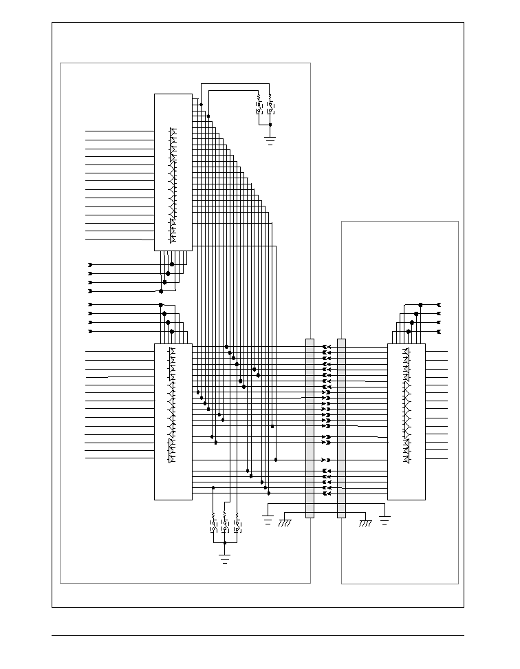
DTE/DCE Serial Port Configuration with the SP504
78
21
79
24
17
22
TxD
TxC
DTR
RTS
RxD
RxC
CTS
DCD
2 3 4 5 12 11 10 9
2 3 4 5 12 11 10 9
14
15
13
16
1
20
80
19
DSR
RI
SCT
LL
RL
ST
78
21
79
24
17
22
61
SD(A)
SD(B)
TT(A)
TT(B)
TR(A)
TR(B)
RS(A)
RS(B)
RT(A)
RT(B)
RD(A)
RD(B)
CS(A)
CS(B)
RR(A)
RR(B)
DM(A)
DM(B)
SCT(A)
SCT(B)
IC(A)
IC(B)
LL(A)
LL(B)
ST(A)
ST(B)
SP504
DTE
Config.
SP504
DCE
Config.
59
63
65
58
56
54
52
70
71
37
38
66
67
35
36
68
69
76
77
39
40
51
49
42
44
61
59
63
65
58
56
54
52
70
71
37
38
66
67
35
36
68
69
76
77
40
39
51
49
42
44
47
RL(A) 47
TxD
TxC
DTR
RTS
RxD
RxC
CTS
DCD
14
15
13
16
1
20
80
19
DSR
RI
SCT
LL
RL
ST
SD(A)
SD(B)
TT(A)
TT(B)
TR(A)
TR(B)
RS(A)
RS(B)
RT(A)
RT(B)
RD(A)
RD(B)
CS(A)
CS(B)
RR(A)
RR(B)
DM(A)
DM(B)
SCT(A)
SCT(B)
IC(A)
IC(B)
LL(A)
ST(A)
ST(B)
RL(A)
LL(B)
0
0
0
0
2 3 4 5 12 11 10 9
14
15
13
16
1
20
80
19
78
21
79
24
17
22
61
59
63
65
58
56
54
52
70
71
37
38
66
67
35
36
68
69
76
77
40
39
51
49
42
44
47
0
1
1
0
TxD
TxC
DTR
RTS
RxD
RxC
CTS
DCD
DSR
RI
SCT
LL
RL
ST
SD(A)
SD(B)
TT(A)
TT(B)
TR(A)
TR(B)
RS(A)
RS(B)
RT(A)
RT(B)
RD(A)
RD(B)
CS(A)
CS(B)
RR(A)
RR(B)
DM(A)
DM(B)
SCT(A)
SCT(B)
IC(A)
IC(B)
LL(A)
LL(B)
ST(A)
ST(B)
RL(A)
SP504
DCE
Config.
0
1
1
0
DB-37 Connector
DB-37 Connector
(V.35 150
termination resistors not shown)

SP504AN
SP504 Application Note
© Copyright 2000 Sipex Corporation
7
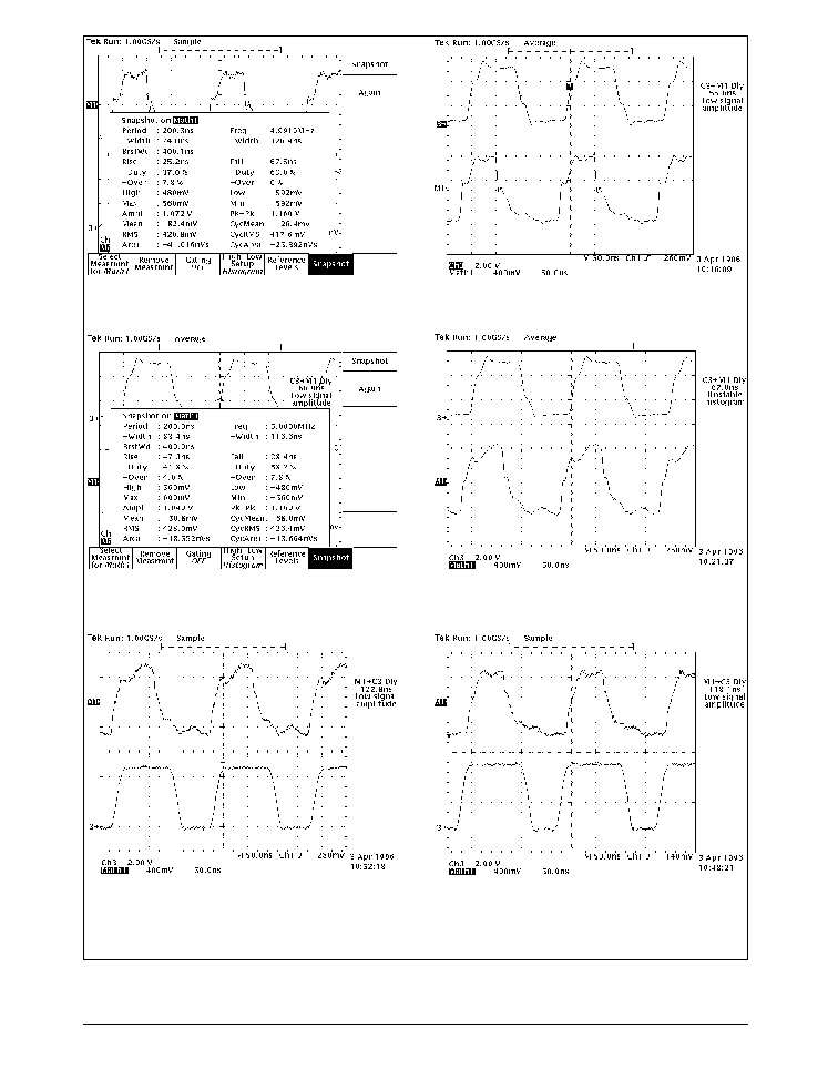
Waveform for TxD Input © Output; DCE, RS-422 mode @ 10Mbps
Waveform for RxD Input © Output; DCE, RS-422 mode @ 10Mbps
Waveform for TxD Input © Output; DTE, RS-422 mode @ 10Mbps
Waveform for RxD Input © Output; DTE, RS-422 mode @ 10Mbps
DRIVER INPUT
DRIVER OUTPUT
DRIVER INPUT
DRIVER OUTPUT
DRIVER INPUT
DRIVER OUTPUT
DRIVER INPUT
DRIVER OUTPUT
SP504AN
SP504 Application Note
© Copyright 2000 Sipex Corporation
8
Waveform for TxD Input © Output; DCE, V.35 mode @ 10Mbps
Waveform for RxD Input © Output; DCE, V.35 mode @ 10Mbps
Waveform for TxD Input © Output; DTE, V.35 mode @ 10Mbps
Waveform for RxD Input © Output; DTE, V.35 mode @ 10Mbps
DRIVER INPUT
DRIVER OUTPUT
DRIVER INPUT
DRIVER OUTPUT
DRIVER INPUT
DRIVER OUTPUT
DRIVER INPUT
DRIVER OUTPUT
SP504AN
SP504 Application Note
© Copyright 2000 Sipex Corporation
9
SP504 - Switching the 150
V.35 Termination Resistor
The SP504 requires one 150
resistor to ground
on each non-inverting (b) driver output. The
150
resistor to ground is necessary to comply
with the V.35 short circuit impedance of
150
±
15
. The resistors will need to be
switched out when V.35 mode is not active. To
perform this, the designer can use one of two
methods: add a relay or switch in series with the
resistor or implant the resistors inside the V.35
cable.
Adding the resistors to the cable is relatively
easy. In DTE mode, two drivers are usually ac-
tive, therefore you will only need two resistors.
The 150
resistors can be connected individu-
ally from pin S (data) to signal ground (pin B)
and pin W (clock) to signal ground (pin B) of
the V.35 ISO-2593 connector.
For DCE applications, an additional driver may
be used for a secondary clock signal. If a cable
is used on the DCE end, a conversion or "mini"
cable is necessary to insert the resistors and route
the proper signals to the DTE cable. The resis-
tors can be connected from pin S (data), pin W
(clock) and an unassigned pin (2nd clock) to sig-
nal ground, pin B. Of course the pins on the
"mini" cable will have to be routed to the appro-
priate end on the DTE V.35 cable. (ie. pin S, pin
W and the unassigned pin will be routed to pin
T, pin X and pin AA, respectively, on the DTE
end.)
Another method is to include the 150
resistors
on the printed circuit board with the SP504 add-
ing switches or relays. This method may be pre-
ferred if a common connector/cable (ie.
DB-25) is used for V.35 and some other mode.
The switches must have low on-resistance, pref-
erably less than 1
. NMOS FETs can be used
as configured on the opposite page. The gate of
the NMOS device is connected to pin 18 of the
SP504. This pin is HIGH when the SP504 is in
V.35 mode and goes LOW in all other modes.
Pin 18 is not described in the data sheet for the
SP504 but can be used to control the switching
of the FETs or relays.
Sipex recommends Siliconix's LITTLE FOOTTM
MOSFET devices such as the Si9959DYTM Dual
N-Channel Enhancement-Mode MOSFET. The
r
DS(on)
is typically less than 0.3
and the devices
are in 8-pin SOIC packages.
TM - LITTLE FOOT is a trademark of Siliconix, member of TEMIC Group.
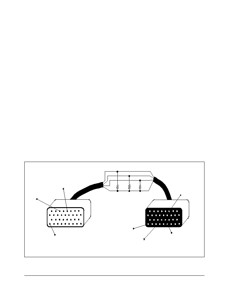
Termination Resistor Implementation in the Cable
W
150
150
150
ISO-2593 male connector
ISO-2593 female connector
S ≠ Transmit Data (b)
W ≠ Terminal Timing (b)
B ≠ Signal Ground
B ≠ Signal Ground
T ≠ Receive Data (b)
X ≠Receive Timing (b)
S
EE
B
T
X
AA
B
AA ≠ Transmit Timing (b)

SP504AN
SP504 Application Note
© Copyright 2000 Sipex Corporation
10
Termination Resistor Implementation on PC Board.
61
59
SP504CF
Drivers
TxD
14
58
DTR
13
54
RTS
16
63
65
TxC
15
42
44
ST
22
47
RL
17
51
LL
24
70
71
RxD
1
37
38
RxC
20
66
CTS
80
68
DSR
78
35
DCD
19
39
RI
21
76
77
SCT
79
Receivers
TDEC
3
9
10
11
12
TDEC
0
TDEC
1
TDEC
2
9
10
11
12
RDEC
0
RDEC
1
RDEC
2
RDEC
3
TxD
DTR
RTS
TxC
ST
RL
LL
Dr
iv
er Decoder
Receiv
er
Decoder
29, 34, 46, 50, 53, 57, 60, 64, 72, 75 GND
22
µ
F
22
µ
F
22
µ
F
25
27 26
30
28
31
32
1N5819
V
CC
V
DD
C1-
C2-
V
SS
C1+
C2+
22
µ
F
+5V
10
µ
F
Pin 18
150
150
150
Pin 18
Pin 18
R
D
R
D
R
D
RxD
RxC
CTS
DSR
DCD
RI
SCT
1
1
1
0

SP504AN
SP504 Application Note
© Copyright 2000 Sipex Corporation
11
ORDERING INFORMATION
Model
Temperature Range
Package Types
SP504CF ............................................... 0
∞
C to +70
∞
C ............................. 80≠pin JEDEC (BE-2 Outline) QFP
Corporation
SIGNAL PROCESSING EXCELLENCE
Sipex Corporation reserves the right to make changes to any products described herein. Sipex does not assume any liability arising out of the
application or use of any product or circuit described hereing; neither does it convey any license under its patent rights nor the rights of others.
Sipex Corporation
Headquarters and
Sales Office
22 Linnell Circle
Billerica, MA 01821
TEL: (978) 667-8700
FAX: (978) 670-9001
e-mail: sales@sipex.com
Sales Office
233 South Hillview Drive
Milpitas, CA 95035
TEL: (408) 934-7500
FAX: (408) 935-7600