 | –≠–ª–µ–∫—Ç—Ä–æ–Ω–Ω—ã–π –∫–æ–º–ø–æ–Ω–µ–Ω—Ç: SP505A | –°–∫–∞—á–∞—Ç—å:  PDF PDF  ZIP ZIP |

1
SP505DS/08
SP505 Multi≠Mode Serial Transceiver
© Copyright 2000 Sipex Corporation
The SP505 is a monolithic device that supports eight (8) popular serial interface standards for DTE to
DCE connectivity. The SP505 is fabricated using a low power BiCMOS process technology, and
incorporates a Sipex patented (5,306,954) charge pump allowing +5V only operation. Seven (7) drivers
and seven (7) receivers can be configured via software for any of the above interface modes at any time.
The SP505 requires no additional external components for compliant operation for all of the eight (8)
modes of operation. All necessary termination is integrated within the SP505 and is switchable when
V.35 drivers, V.35 receivers, and V.11 receivers are used. The SP505 can operate as either a DTE or DCE.
Additional features with the SP505 include internal loopback that can be initiated in either single-ended
or differential modes. While in loopback mode, driver outputs are internally connected to receiver inputs
creating an internal signal path convenient for diagnostic testing. This eliminates the need for an external
loopback plug. The SP505 also includes a latch enable pin with the driver and receiver address decoder.
Tri-state ability for the driver and receiver outputs is controlled by supplying a 4-bit word into the address
decoder. Seven (7) drivers and one (1) receiver in the SP505 include separate enable pins for added
convenience. The SP505 is ideal for WAN serial ports in networking equipment such as routers,
switches, DSU/CSU's, and other access devices.
SP505
WAN Multi-Mode Serial Transceiver
DESCRIPTION...
s
+5V Only Operation
s
Seven (7) Drivers and Seven (7) Receivers
s
Driver and Receiver Tri-state Control
s
Internal Transceiver Termination Resistors for
V.11 and V.35 Protocols
s
Loopback Self-Test Mode
s
Software Selectable Protocol Selection
s
Interface Modes Supported:
RS-232
(V.28)
X.21/RS-422
(V.11)
EIA-530
(V.10 & V.11)
EIA-530A
(V.10 & V.11)
RS-449
(V.10 & V.11)
V.35
(V.35 & V.28)
V.36
(V.10 & V.11)
RS-485
(un-terminated V.11)
s
Improved ESD Tolerance for Analog I/Os
s
High Differential Transmission Rates
Ø
SP505A - 10Mbps
Ø
SP505B - over 16Mbps
s
Compliant to NET1/2 and TBR2 Physical
Layer Requirements
(TUV Test Report NET2/052101/98)
(TUV Test Report CTR2/052101/98)
EIA-530
WAN
V.35
Æ

2
SP505DS/08
SP505 Multi≠Mode Serial Transceiver
© Copyright 2000 Sipex Corporation
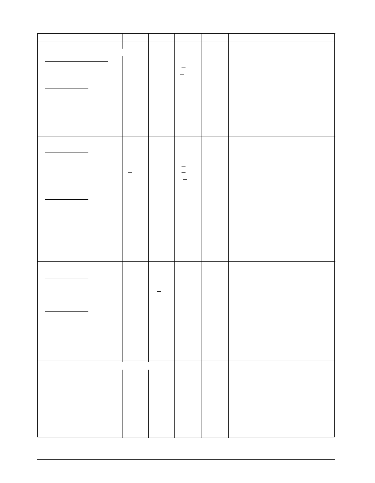
SPECIFICATIONS
T
A
= +25
∞
C and V
CC
= +4.75V to +5.25V unless otherwise noted.
MIN.
TYP.
MAX.
UNITS
CONDITIONS
LOGIC INPUTS
V
IL
0.8
Volts
V
IH
2.0
Volts
LOGIC OUTPUTS
V
OL
0.4
Volts
I
OUT
= ≠3.2mA
V
OH
2.4
Volts
I
OUT
= 1.0mA
V.28 DRIVER
DC Parameters
Outputs
Open Circuit Voltage
+15
Volts
per Figure 1
Loaded Voltage
+5.0
+15
Volts
per Figure 2
Short-Circuit Current
+100
mA
per Figure 4
Power-Off Impedance
300
per Figure 5
AC Parameters
V
CC
= +5V for AC parameters
Outputs
Transition Time
1.5
µ
s
per Figure 6; +3V to -3V
Instantaneous Slew Rate
30
V/
µ
s
per Figure 3
Propagation Delay
t
PHL
0.5
1
5
µ
s
t
PLH
0.5
1
5
µ
s
Max.Transmission Rate
120
230
kbps
V.28 RECEIVER
DC Parameters
Inputs
Input Impedance
3
7
k
per Figure 7
Open-Circuit Bias
+2.0
Volts
per Figure 8
HIGH Threshold
1.7
3.0
Volts
LOW Threshold
0.8
1.2
Volts
AC Parameters
V
CC
= +5V for AC parameters
Propagation Delay
t
PHL
50
100
500
ns
t
PLH
50
100
500
ns
ABSOLUTE MAXIMUM RATINGS
These are stress ratings only and functional operation
of the device at these ratings or any other above those
indicated in the operation sections of the specifications
below is not implied. Exposure to absolute maximum
rating conditions for extended periods of time may
affect reliability.
V
CC
............................................................................+7V
Input Voltages:
Logic...............................-0.3V to (V
CC
+0.5V)
Drivers............................-0.3V to (V
CC
+0.5V)
Receivers........................................
±
15.5V
Output Voltages:
Logic................................-0.3V to (V
CC
+0.5V)
Drivers................................................
±
15V
Receivers........................-0.3V to (V
CC
+0.5V)
Storage Temperature..........................-65∞C to +150∞C
Power Dissipation.........................................2000mW
Package Derating:
¯
JA
....................................................46
∞
C/W
¯
JC
...................................................16
∞
C/W
STORAGE CONSIDERATIONS
Due to the relatively large package size of the 80-pin
quad flat-pack, storage in a low humidity environment
is preferred. Large high density plastic packages are
moisture sensitive and should be stored in Dry Vapor
Barrier Bags. Prior to usage, the parts should remain
bagged and stored below 40
∞
C and 60%RH. If the
parts are removed from the bag, they should be used
within 48 hours or stored in an environment at or below
20%RH. If the above conditions cannot be followed,
the parts should be baked for four hours at 125
∞
C in
order remove moisture prior to soldering. Sipex ships
the 80-pin QFP in Dry Vapor Barrier Bags with a
humidity indicator card and desiccant pack. The
humidity indicator should be below 30%RH.

3
SP505DS/08
SP505 Multi≠Mode Serial Transceiver
© Copyright 2000 Sipex Corporation
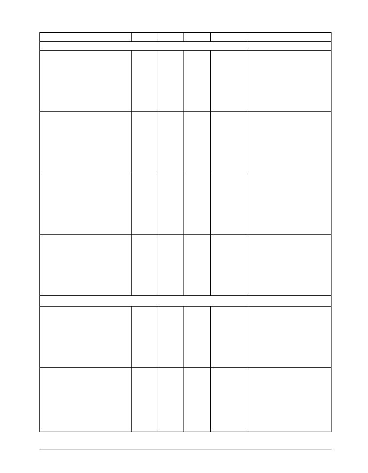
SPECIFICATIONS
T
A
= +25
∞
C and V
CC
= +4.75V to +5.25V unless otherwise noted.
MIN.
TYP.
MAX.
UNITS
CONDITIONS
V.28 RECEIVER (continued)
AC Parameters (cont.)
Max.Transmission Rate
120
230
kbps
V.10 DRIVER
DC Parameters
Outputs
Open Circuit Voltage
+4.0
+6.0
Volts
per Figure 9
Test-Terminated Voltage
0.9V
OC
Volts
per Figure 10
Short-Circuit Current
+150
mA
per Figure 11
Power-Off Current
+100
µ
A
per Figure 12
AC Parameters
V
CC
= +5V for AC parameters
Outputs
Transition Time
200
ns
per Figure 13; 10% to 90%
Propagation Delay
t
PHL
50
100
500
ns
t
PLH
50
100
500
ns
Max.Transmission Rate
120
kbps
V.10 RECEIVER
DC Parameters
Inputs
Input Current
≠3.25
+3.25
mA
per Figures 14 and 15
Input Impedance
4
k
Sensitivity
+0.3
Volts
AC Parameters
V
CC
= +5V for AC parameters
Propagation Delay
t
PHL
50
120
250
ns
t
PLH
50
120
250
ns
Max.Transmission Rate
120
kbps
V.11 DRIVER
DC Parameters
Outputs
Open Circuit Voltage
+5.0
Volts
per Figure 16
Test Terminated Voltage
+2.0
Volts
per Figure 17
0.5V
OC
0.67V
OC
Volts
Balance
+0.4
Volts
per Figure 17
Offset
+3.0
Volts
per Figure 17
Short-Circuit Current
+150
mA
per Figure 18
Power-Off Current
+100
µ
A
per Figure 19
AC Parameters
V
CC
= +5V for AC parameters
Outputs
Transition Time
20
ns
per Figures 21 and 36; 10% to 90%
Propagation Delay
t
PHL
50
85
110
ns
per Figures 33 and 36, C
L
= 50pF
t
PLH
50
85
110
ns
per Figures 33 and 36, C
L
= 50pF
Differential Skew
10
20
ns
per Figures 33 and 36, C
L
= 50pF
Max.Transmission Rate
per Figure 33, C
L
= 50pF
SP505ACF
10
12
Mbps
f
IN
= 5MHz
SP505BCF
16.4
18
Mbps
f
IN
= 8.2MHz
V.11 RECEIVER
DC Parameters
Inputs
Common Mode Range
≠7
+7
Volts
Sensitivity
+0.3
Volts
4
SP505DS/08
SP505 Multi≠Mode Serial Transceiver
© Copyright 2000 Sipex Corporation
SPECIFICATIONS
T
A
= +25
∞
C and V
CC
= +4.75V to +5.25V unless otherwise noted.
MIN.
TYP.
MAX.
UNITS
CONDITIONS
V.11 RECEIVER (continued)
DC Parameters (cont.)
Input Current
≠3.25
+3.25
mA
per Figure 20 and 22
Current w/ 100
Termination
+60.75
mA
per Figure 23 and 24
Input Impedance
4
k
AC Parameters
V
CC
= +5V for AC parameters
Propagation Delay
t
PHL
80
110
130
ns
per Figures 33 and 38; C
L
= 50pF
t
PLH
80
110
130
ns
per Figures 33 and 38; C
L
= 50pF
Differential Skew
20
ns
per Figure 33; C
L
= 50pF
Max.Transmission Rate
per Figure 33; C
L
= 50pF
SP505ACF
10
12
Mbps
f
IN
= 5MHz
SP505BCF
16.4
18
Mbps
f
IN
= 8.2MHz
V.35 DRIVER
DC Parameters
Outputs
Open Circuit Voltage
+1.20
Volts
per Figure 16
Test Terminated Voltage
+0.44
+0.66
Volts
per Figure 25
Offset
+0.6
Volts
per Figure 25
Source Impedance
50
150
per Figure 27; Z
S
= V
2
/V
1
x 50
Short-Circuit Impedance
135
165
per Figure 28
AC Parameters
V
CC
= +5V for AC parameters
Outputs
Transition Time
30
40
ns
per Figure 29; 10% to 90%
Propagation Delay
t
PHL
50
90
110
ns
per Figures 33 and 36; C
L
= 20pF
t
PLH
50
90
110
ns
per Figures 33 and 36; C
L
= 20pF
Differential Skew
20
30
ns
per Figures 33 and 36; C
L
= 20pF
Max.Transmission Rate
per Figure 33; C
L
= 20pF
SP505ACF
10
12
Mbps
f
IN
= 5MHz
SP505BCF
16.4
18
Mbps
f
IN
= 8.2MHz
V.35 RECEIVER
DC Parameters
Inputs
Sensitivity
+80
mV
Source Impedance
90
110
per Figure 30; Z
S
= V
2
/V
1
x 50
Short-Circuit Impedance
135
165
per Figure 31
AC Parameters
V
CC
= +5V for AC parameters
Propagation Delay
t
PHL
80
110
130
ns
per Figures 33 and 38; C
L
= 20pF
t
PLH
80
110
130
ns
per Figures 33 and 38; C
L
= 20pF
Differential Skew
20
ns
per Figure 33; C
L
= 20pF
Max.Transmission Rate
per Figure 33; C
L
= 20pF
SP505ACF
10
12
Mbps
f
IN
= 5MHz
SP505BCF
16.4
18
Mbps
f
IN
= 8.2MHz
TRANSCEIVER LEAKAGE CURRENTS
Driver Output 3-State Current
100
500
µ
A
per Figure 32; Drivers disabled
Rcvr Output 3-State Current
1
10
µ
A
DEC
X
= 0000, 0.4V
V
O
2.4V
5
SP505DS/08
SP505 Multi≠Mode Serial Transceiver
© Copyright 2000 Sipex Corporation
OTHER AC CHARACTERISTICS
T
A
= +25
∞
C and V
CC
= +5.0V unless otherwise noted.
PARAMETER
MIN.
TYP.
MAX.
UNITS
CONDITIONS
DRIVER DELAY TIME BETWEEN ACTIVE MODE AND TRI-STATE MODE
RS-232/V.28
t
PZL
; Tri-state to Output LOW
0.70
5.0
µ
s
C
L
= 100pF, Fig. 34 & 40; S
1
closed
t
PZH
; Tri-state to Output HIGH
0.40
2.0
µ
s
C
L
= 100pF, Fig. 34 & 40; S
2
closed
t
PLZ
; Output LOW to Tri-state
0.20
2.0
µ
s
C
L
= 100pF, Fig. 34 & 40; S
1
closed
t
PHZ
; Output HIGH to Tri-state
0.40
2.0
µ
s
C
L
= 100pF, Fig. 34 & 40; S
2
closed
RS-423/V.10
t
PZL
; Tri-state to Output LOW
0.15
2.0
µ
s
C
L
= 100pF, Fig. 34 & 40; S
1
closed
t
PZH
; Tri-state to Output HIGH
0.20
2.0
µ
s
C
L
= 100pF, Fig. 34 & 40; S
2
closed
t
PLZ
; Output LOW to Tri-state
0.20
2.0
µ
s
C
L
= 100pF, Fig. 34 & 40; S
1
closed
t
PHZ
; Output HIGH to Tri-state
0.15
2.0
µ
s
C
L
= 100pF, Fig. 34 & 40; S
2
closed
RS-422/V.11
t
PZL
; Tri-state to Output LOW
2.80
10.0
µ
s
C
L
= 100pF, Fig. 34 & 37; S
1
closed
t
PZH
; Tri-state to Output HIGH
0.10
2.0
µ
s
C
L
= 100pF, Fig. 34 & 37; S
2
closed
t
PLZ
; Output LOW to Tri-state
0.10
2.0
µ
s
C
L
= 15pF, Fig. 34 & 37; S
1
closed
t
PHZ
; Output HIGH to Tri-state
0.10
2.0
µ
s
C
L
= 15pF, Fig. 34 & 37; S
2
closed
V.35
t
PZL
; Tri-state to Output LOW
2.60
10.0
µ
s
C
L
= 100pF, Fig. 34 & 37; S
1
closed
t
PZH
; Tri-state to Output HIGH
0.10
2.0
µ
s
C
L
= 100pF, Fig. 34 & 37; S
2
closed
t
PLZ
; Output LOW to Tri-state
0.10
2.0
µ
s
C
L
= 15pF, Fig. 34 & 37; S
1
closed
t
PHZ
; Output HIGH to Tri-state
0.15
2.0
µ
s
C
L
= 15pF, Fig. 34 & 37; S
2
closed
RECEIVER DELAY TIME BETWEEN ACTIVE MODE AND TRI-STATE MODE
RS-232/V.28
t
PZL
; Tri-state to Output LOW
0.12
2.0
µ
s
C
L
= 100pF, Fig. 35 & 38; S
1
closed
t
PZH
; Tri-state to Output HIGH
0.10
2.0
µ
s
C
L
= 100pF, Fig. 35 & 38; S
2
closed
t
PLZ
; Output LOW to Tri-state
0.10
2.0
µ
s
C
L
= 100pF, Fig. 35 & 38; S
1
closed
t
PHZ
; Output HIGH to Tri-state
0.10
2.0
µ
s
C
L
= 100pF, Fig. 35 & 38; S
2
closed
RS-423/V.10
t
PZL
; Tri-state to Output LOW
0.10
2.0
µ
s
C
L
= 100pF, Fig. 35 & 38; S
1
closed
t
PZH
; Tri-state to Output HIGH
0.10
2.0
µ
s
C
L
= 100pF, Fig. 35 & 38; S
2
closed
t
PLZ
; Output LOW to Tri-state
0.10
2.0
µ
s
C
L
= 100pF, Fig. 35 & 38; S
1
closed
t
PHZ
; Output HIGH to Tri-state
0.10
2.0
µ
s
C
L
= 100pF, Fig. 35 & 38; S
2
closed