 | –≠–ª–µ–∫—Ç—Ä–æ–Ω–Ω—ã–π –∫–æ–º–ø–æ–Ω–µ–Ω—Ç: SP505ACF | –°–∫–∞—á–∞—Ç—å:  PDF PDF  ZIP ZIP |

1
Rev: A Date: 1/27/04
SP505 Multi≠Mode Serial Transceiver
© Copyright 2004 Sipex Corporation
The SP505 is a monolithic device that supports eight (8) popular serial interface standards for DTE to
DCE connectivity. The SP505 is fabricated using a low power BiCMOS process technology, and
incorporates a Sipex patented (5,306,954) charge pump allowing +5V only operation. Seven (7) drivers
and seven (7) receivers can be configured via software for any of the above interface modes at any time.
The SP505 requires no additional external components for compliant operation for all of the eight (8)
modes of operation. All necessary termination is integrated within the SP505 and is switchable when
V.35 drivers, V.35 receivers, and V.11 receivers are used. The SP505 can operate as either a DTE or DCE.
Additional features with the SP505 include internal loopback that can be initiated in either single-ended
or differential modes. While in loopback mode, driver outputs are internally connected to receiver inputs
creating an internal signal path convenient for diagnostic testing. This eliminates the need for an external
loopback plug. The SP505 also includes a latch enable pin with the driver and receiver address decoder.
Tri-state ability for the driver and receiver outputs is controlled by supplying a 4-bit word into the address
decoder. Seven (7) drivers and one (1) receiver in the SP505 include separate enable pins for added
convenience. The SP505 is ideal for WAN serial ports in networking equipment such as routers,
switches, DSU/CSU's, and other access devices.
SP505
WAN Multi-Mode Serial Transceiver
DESCRIPTION...
+5V Only Operation
Seven (7) Drivers and Seven (7) Receivers
Driver and Receiver Tri-state Control
Internal Transceiver Termination Resistors for
V.11 and V.35 Protocols
Loopback Self-Test Mode
Software Selectable Protocol Selection
Interface Modes Supported:
RS-232
(V.28)
X.21/RS-422
(V.11)
EIA-530
(V.10 & V.11)
EIA-530A
(V.10 & V.11)
RS-449
(V.10 & V.11)
V.35
(V.35 & V.28)
V.36
(V.10 & V.11)
RS-485
(un-terminated V.11)
Improved ESD Tolerance for Analog I/Os
High Differential Transmission Rates
SP505A - 10Mbps
SP505B - over 16Mbps
Compliant to NET1/2 and TBR2 Physical
Layer Requirements
(TUV Test Report NET2/052101/98)
(TUV Test Report CTR2/052101/98)
EIA-530
WAN
V.35
Æ

2
Rev: A Date: 1/27/04
SP505 Multi≠Mode Serial Transceiver
© Copyright 2004 Sipex Corporation
SPECIFICATIONS
T
A
= +25∞C and V
CC
= +4.75V to +5.25V unless otherwise noted.
MIN.
TYP.
MAX.
UNITS
CONDITIONS
LOGIC INPUTS
V
IL
0.8
Volts
V
IH
2.0
Volts
LOGIC OUTPUTS
V
OL
0.4
Volts
I
OUT
= ≠3.2mA
V
OH
2.4
Volts
I
OUT
= 1.0mA
V.28 DRIVER
DC Parameters
Outputs
Open Circuit Voltage
+15
Volts
per Figure 1
Loaded Voltage
+5.0
+15
Volts
per Figure 2
Short-Circuit Current
+100
mA
per Figure 4
Power-Off Impedance
300
per Figure 5
AC Parameters
V
CC
= +5V for AC parameters
Outputs
Transition Time
1.5
µ
s
per Figure 6; +3V to -3V
Instantaneous Slew Rate
30
V/
µ
s
per Figure 3
Propagation Delay
t
PHL
0.5
1
5
µ
s
t
PLH
0.5
1
5
µ
s
Max.Transmission Rate
120
230
kbps
V.28 RECEIVER
DC Parameters
Inputs
Input Impedance
3
7
k
per Figure 7
Open-Circuit Bias
+2.0
Volts
per Figure 8
HIGH Threshold
1.7
3.0
Volts
LOW Threshold
0.8
1.2
Volts
AC Parameters
V
CC
= +5V for AC parameters
Propagation Delay
t
PHL
50
100
500
ns
t
PLH
50
100
500
ns
ABSOLUTE MAXIMUM RATINGS
These are stress ratings only and functional operation
of the device at these ratings or any other above those
indicated in the operation sections of the specifications
below is not implied. Exposure to absolute maximum
rating conditions for extended periods of time may
affect reliability.
V
CC
............................................................................+7V
Input Voltages:
Logic...............................-0.3V to (V
CC
+0.5V)
Drivers............................-0.3V to (V
CC
+0.5V)
Receivers........................................±15.5V
Output Voltages:
Logic................................-0.3V to (V
CC
+0.5V)
Drivers................................................±15V
Receivers........................-0.3V to (V
CC
+0.5V)
Storage Temperature..........................-65∞C to +150∞C
Power Dissipation.........................................2000mW
Package Derating:
¯
JA
....................................................46 ∞C/W
¯
JC
...................................................16 ∞C/W
STORAGE CONSIDERATIONS
Due to the relatively large package size of the 80-pin
quad flat-pack, storage in a low humidity environment
is preferred. Large high density plastic packages are
moisture sensitive and should be stored in Dry Vapor
Barrier Bags. Prior to usage, the parts should remain
bagged and stored below 40∞C and 60%RH. If the
parts are removed from the bag, they should be used
within 48 hours or stored in an environment at or below
20%RH. If the above conditions cannot be followed,
the parts should be baked for four hours at 125∞C in
order remove moisture prior to soldering. Sipex ships
the 80-pin QFP in Dry Vapor Barrier Bags with a
humidity indicator card and desiccant pack. The
humidity indicator should be below 30%RH.

3
Rev: A Date: 1/27/04
SP505 Multi≠Mode Serial Transceiver
© Copyright 2004 Sipex Corporation
SPECIFICATIONS
T
A
= +25∞C and V
CC
= +4.75V to +5.25V unless otherwise noted.
MIN.
TYP.
MAX.
UNITS
CONDITIONS
V.28 RECEIVER (continued)
AC Parameters (cont.)
Max.Transmission Rate
120
230
kbps
V.10 DRIVER
DC Parameters
Outputs
Open Circuit Voltage
+4.0
+6.0
Volts
per Figure 9
Test-Terminated Voltage
0.9V
OC
Volts
per Figure 10
Short-Circuit Current
+150
mA
per Figure 11
Power-Off Current
+100
µ
A
per Figure 12
AC Parameters
V
CC
= +5V for AC parameters
Outputs
Transition Time
200
ns
per Figure 13; 10% to 90%
Propagation Delay
t
PHL
50
100
500
ns
t
PLH
50
100
500
ns
Max.Transmission Rate
120
kbps
V.10 RECEIVER
DC Parameters
Inputs
Input Current
≠3.25
+3.25
mA
per Figures 14 and 15
Input Impedance
4
k
Sensitivity
+0.3
Volts
AC Parameters
V
CC
= +5V for AC parameters
Propagation Delay
t
PHL
50
120
250
ns
t
PLH
50
120
250
ns
Max.Transmission Rate
120
kbps
V.11 DRIVER
DC Parameters
Outputs
Open Circuit Voltage
+5.0
Volts
per Figure 16
Test Terminated Voltage
+2.0
Volts
per Figure 17
0.5V
OC
0.67V
OC
Volts
Balance
+0.4
Volts
per Figure 17
Offset
+3.0
Volts
per Figure 17
Short-Circuit Current
+150
mA
per Figure 18
Power-Off Current
+100
µ
A
per Figure 19
AC Parameters
V
CC
= +5V for AC parameters
Outputs
Transition Time
20
ns
per Figures 21 and 36; 10% to 90%
Propagation Delay
t
PHL
50
85
110
ns
per Figures 33 and 36, C
L
= 50pF
t
PLH
50
85
110
ns
per Figures 33 and 36, C
L
= 50pF
Differential Skew
10
20
ns
per Figures 33 and 36, C
L
= 50pF
Max.Transmission Rate
per Figure 33, C
L
= 50pF
SP505ACF
10
12
Mbps
f
IN
= 5MHz
SP505BCF
16.4
18
Mbps
f
IN
= 8.2MHz
V.11 RECEIVER
DC Parameters
Inputs
Common Mode Range
≠7
+7
Volts
Sensitivity
+0.3
Volts
4
Rev: A Date: 1/27/04
SP505 Multi≠Mode Serial Transceiver
© Copyright 2004 Sipex Corporation
SPECIFICATIONS
T
A
= +25∞C and V
CC
= +4.75V to +5.25V unless otherwise noted.
MIN.
TYP.
MAX.
UNITS
CONDITIONS
V.11 RECEIVER (continued)
DC Parameters (cont.)
Input Current
≠3.25
+3.25
mA
per Figure 20 and 22
Current w/ 100 Termination
+60.75
mA
per Figure 23 and 24
Input Impedance
4
k
AC Parameters
V
CC
= +5V for AC parameters
Propagation Delay
t
PHL
80
110
130
ns
per Figures 33 and 38; C
L
= 50pF
t
PLH
80
110
130
ns
per Figures 33 and 38; C
L
= 50pF
Differential Skew
20
ns
per Figure 33; C
L
= 50pF
Max.Transmission Rate
per Figure 33; C
L
= 50pF
SP505ACF
10
12
Mbps
f
IN
= 5MHz
SP505BCF
16.4
18
Mbps
f
IN
= 8.2MHz
V.35 DRIVER
DC Parameters
Outputs
Open Circuit Voltage
+1.20
Volts
per Figure 16
Test Terminated Voltage
+0.44
+0.66
Volts
per Figure 25
Offset
+0.6
Volts
per Figure 25
Source Impedance
50
150
per Figure 27; Z
S
= V
2
/V
1
x 50
Short-Circuit Impedance
135
165
per Figure 28
AC Parameters
V
CC
= +5V for AC parameters
Outputs
Transition Time
30
40
ns
per Figure 29; 10% to 90%
Propagation Delay
t
PHL
50
90
110
ns
per Figures 33 and 36; C
L
= 20pF
t
PLH
50
90
110
ns
per Figures 33 and 36; C
L
= 20pF
Differential Skew
20
30
ns
per Figures 33 and 36; C
L
= 20pF
Max.Transmission Rate
per Figure 33; C
L
= 20pF
SP505ACF
10
12
Mbps
f
IN
= 5MHz
SP505BCF
16.4
18
Mbps
f
IN
= 8.2MHz
V.35 RECEIVER
DC Parameters
Inputs
Sensitivity
+80
mV
Source Impedance
90
110
per Figure 30; Z
S
= V
2
/V
1
x 50
Short-Circuit Impedance
135
165
per Figure 31
AC Parameters
V
CC
= +5V for AC parameters
Propagation Delay
t
PHL
80
110
130
ns
per Figures 33 and 38; C
L
= 20pF
t
PLH
80
110
130
ns
per Figures 33 and 38; C
L
= 20pF
Differential Skew
20
ns
per Figure 33; C
L
= 20pF
Max.Transmission Rate
per Figure 33; C
L
= 20pF
SP505ACF
10
12
Mbps
f
IN
= 5MHz
SP505BCF
16.4
18
Mbps
f
IN
= 8.2MHz
TRANSCEIVER LEAKAGE CURRENTS
Driver Output 3-State Current
100
500
µ
A
per Figure 32; Drivers disabled
Rcvr Output 3-State Current
1
10
µ
A
DEC
X
= 0000, 0.4V V
O
2.4V

5
Rev: A Date: 1/27/04
SP505 Multi≠Mode Serial Transceiver
© Copyright 2004 Sipex Corporation
OTHER AC CHARACTERISTICS
T
A
= +25∞C and V
CC
= +5.0V unless otherwise noted.
PARAMETER
MIN.
TYP.
MAX.
UNITS
CONDITIONS
DRIVER DELAY TIME BETWEEN ACTIVE MODE AND TRI-STATE MODE
RS-232/V.28
t
PZL
; Tri-state to Output LOW
0.70
5.0
µ
s
C
L
= 100pF, Fig. 34 & 40; S
1
closed
t
PZH
; Tri-state to Output HIGH
0.40
2.0
µ
s
C
L
= 100pF, Fig. 34 & 40; S
2
closed
t
PLZ
; Output LOW to Tri-state
0.20
2.0
µ
s
C
L
= 100pF, Fig. 34 & 40; S
1
closed
t
PHZ
; Output HIGH to Tri-state
0.40
2.0
µ
s
C
L
= 100pF, Fig. 34 & 40; S
2
closed
RS-423/V.10
t
PZL
; Tri-state to Output LOW
0.15
2.0
µ
s
C
L
= 100pF, Fig. 34 & 40; S
1
closed
t
PZH
; Tri-state to Output HIGH
0.20
2.0
µ
s
C
L
= 100pF, Fig. 34 & 40; S
2
closed
t
PLZ
; Output LOW to Tri-state
0.20
2.0
µ
s
C
L
= 100pF, Fig. 34 & 40; S
1
closed
t
PHZ
; Output HIGH to Tri-state
0.15
2.0
µ
s
C
L
= 100pF, Fig. 34 & 40; S
2
closed
RS-422/V.11
t
PZL
; Tri-state to Output LOW
2.80
10.0
µ
s
C
L
= 100pF, Fig. 34 & 37; S
1
closed
t
PZH
; Tri-state to Output HIGH
0.10
2.0
µ
s
C
L
= 100pF, Fig. 34 & 37; S
2
closed
t
PLZ
; Output LOW to Tri-state
0.10
2.0
µ
s
C
L
= 15pF, Fig. 34 & 37; S
1
closed
t
PHZ
; Output HIGH to Tri-state
0.10
2.0
µ
s
C
L
= 15pF, Fig. 34 & 37; S
2
closed
V.35
t
PZL
; Tri-state to Output LOW
2.60
10.0
µ
s
C
L
= 100pF, Fig. 34 & 37; S
1
closed
t
PZH
; Tri-state to Output HIGH
0.10
2.0
µ
s
C
L
= 100pF, Fig. 34 & 37; S
2
closed
t
PLZ
; Output LOW to Tri-state
0.10
2.0
µ
s
C
L
= 15pF, Fig. 34 & 37; S
1
closed
t
PHZ
; Output HIGH to Tri-state
0.15
2.0
µ
s
C
L
= 15pF, Fig. 34 & 37; S
2
closed
RECEIVER DELAY TIME BETWEEN ACTIVE MODE AND TRI-STATE MODE
RS-232/V.28
t
PZL
; Tri-state to Output LOW
0.12
2.0
µ
s
C
L
= 100pF, Fig. 35 & 38; S
1
closed
t
PZH
; Tri-state to Output HIGH
0.10
2.0
µ
s
C
L
= 100pF, Fig. 35 & 38; S
2
closed
t
PLZ
; Output LOW to Tri-state
0.10
2.0
µ
s
C
L
= 100pF, Fig. 35 & 38; S
1
closed
t
PHZ
; Output HIGH to Tri-state
0.10
2.0
µ
s
C
L
= 100pF, Fig. 35 & 38; S
2
closed
RS-423/V.10
t
PZL
; Tri-state to Output LOW
0.10
2.0
µ
s
C
L
= 100pF, Fig. 35 & 38; S
1
closed
t
PZH
; Tri-state to Output HIGH
0.10
2.0
µ
s
C
L
= 100pF, Fig. 35 & 38; S
2
closed
t
PLZ
; Output LOW to Tri-state
0.10
2.0
µ
s
C
L
= 100pF, Fig. 35 & 38; S
1
closed
t
PHZ
; Output HIGH to Tri-state
0.10
2.0
µ
s
C
L
= 100pF, Fig. 35 & 38; S
2
closed

6
Rev: A Date: 1/27/04
SP505 Multi≠Mode Serial Transceiver
© Copyright 2004 Sipex Corporation
POWER REQUIREMENTS
PARAMETER
MIN.
TYP.
MAX.
UNITS
CONDITIONS
V
CC
4.75
5.00
5.25
Volts
I
CC
(No Mode Selected)
30
mA
All I
CC
values are with V
CC
= +5V,
(V.28/RS-232)
60
mA
T = +25
o
C, all drivers are loaded to
(V.11/RS-422)
300
mA
their specified maximum load and all
(RS-449)
250
mA
drivers are active at their maximum
(V.35)
105
mA
specified data transmission rates.
EIA-530
260
mA
EIA-530A
250
mA
V.36
65
mA
OTHER AC CHARACTERISTICS
(Continued)
T
A
= +25∞C and V
CC
= +5.0V unless otherwise noted.
PARAMETER
MIN.
TYP.
MAX.
UNITS
CONDITIONS
RS-422/V.11
t
PZL
; Tri-state to Output LOW
0.10
2.0
µ
s
C
L
= 100pF, Fig. 35 & 39; S
1
closed
t
PZH
; Tri-state to Output HIGH
0.10
2.0
µ
s
C
L
= 100pF, Fig. 35 & 39; S
2
closed
t
PLZ
; Output LOW to Tri-state
0.10
2.0
µ
s
C
L
= 15pF, Fig. 35 & 39; S
1
closed
t
PHZ
; Output HIGH to Tri-state
0.10
2.0
µ
s
C
L
= 15pF, Fig. 35 & 39; S
2
closed
V.35
t
PZL
; Tri-state to Output LOW
0.10
2.0
µ
s
C
L
= 100pF, Fig. 35 & 39; S
1
closed
t
PZH
; Tri-state to Output HIGH
0.10
2.0
µ
s
C
L
= 100pF, Fig. 35 & 39; S
2
closed
t
PLZ
; Output LOW to Tri-state
0.10
2.0
µ
s
C
L
= 15pF, Fig. 35 & 39; S
1
closed
t
PHZ
; Output HIGH to Tri-state
0.10
2.0
µ
s
C
L
= 15pF, Fig. 35 & 39; S
2
closed
TRANSCEIVER TO TRANSCEIVER SKEW
(per Figures 33, 36, 38)
V.28 Driver
100
ns
| (t
phl
)
Tx1
≠ (t
phl
)
Tx6,7
|
100
ns
| (t
plh
)
Tx1
≠ (t
plh
)
Tx6,7
|
V.28 Receiver
20
ns
| (t
phl
)
Rx1
≠ (t
phl
)
Rx2,7
|
20
ns
| (t
phl
)
Rx1
≠ (t
phl
)
Rx2,7
|
V.11 Driver
2
ns
| (t
phl
)
Tx1
≠ (t
phl
)
Tx6,7
|
2
ns
| (t
plh
)
Tx1
≠ (t
plh
)
Tx6,7
|
V.11 Receiver
3
ns
| (t
phl
)
Rx1
≠ (t
phl
)
Rx2,7
|
3
ns
| (t
phl
)
Rx1
≠ (t
phl
)
Rx2,7
|
V.10 Driver
5
ns
| (t
phl
)
Tx2
≠ (t
phl
)
Tx3,4,5
|
5
ns
| (t
plh
)
Tx2
≠ (t
plh
)
Tx3,4,5
|
V.10 Receiver
5
ns
| (t
phl
)
Rx2
≠ (t
phl
)
Rx3,4,5
|
5
ns
| (t
phl
)
Rx2
≠ (t
phl
)
Rx3,4,5
|
V.35 Driver
4
ns
| (t
phl
)
Tx1
≠ (t
phl
)
Tx6,7
|
4
ns
| (t
plh
)
Tx1
≠ (t
plh
)
Tx6,7
|
V.35 Receiver
6
ns
| (t
phl
)
Rx1
≠ (t
phl
)
Rx2,7
|
6
ns
| (t
phl
)
Rx1
≠ (t
phl
)
Rx2,7
|

7
Rev: A Date: 1/27/04
SP505 Multi≠Mode Serial Transceiver
© Copyright 2004 Sipex Corporation
A
V
OC
C
A
V
T
C
3k
A
V
T
C
7k
Oscilloscope
Scope used for slew rate
measurement.
A
I
sc
C
A
C
V
CC
= 0V
±
2V
I
x
A
C
3k
2500pF
Oscilloscope
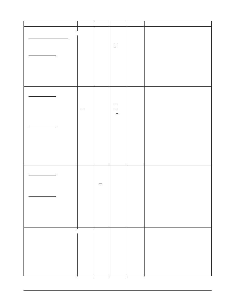
Figure 1. V.28 Driver Output Open Circuit Voltage
Figure 2. V.28 Driver Output Loaded Voltage
Figure 3. V.28 Driver Output Slew Rate
Figure 4. V.28 Driver Output Short-Circuit Current
Figure 6. V.28 Driver Output Rise/Fall Times
Figure 5. V.28 Driver Output Power-Off Impedance
TEST CIRCUITS...

8
Rev: A Date: 1/27/04
SP505 Multi≠Mode Serial Transceiver
© Copyright 2004 Sipex Corporation
Figure 7. V.28 Receiver Input Impedance
A
C
I
ia
±
15V
A
C
V
oc
Figure 8. V.28 Receiver Input Open Circuit Bias
A
V
OC
3.9k
C
A
V
t
450
C
A
C
±
0.25V
V
CC
= 0V
I
x
A
I
sc
C
Figure 9. V.10 Driver Output Open-Circuit Voltage
Figure 10. V.10 Driver Output Test Terminated Voltage
Figure 12. V.10 Driver Output Power-Off Current
Figure 11. V.10 Driver Output Short-Circuit Current
9
Rev: A Date: 1/27/04
SP505 Multi≠Mode Serial Transceiver
© Copyright 2004 Sipex Corporation
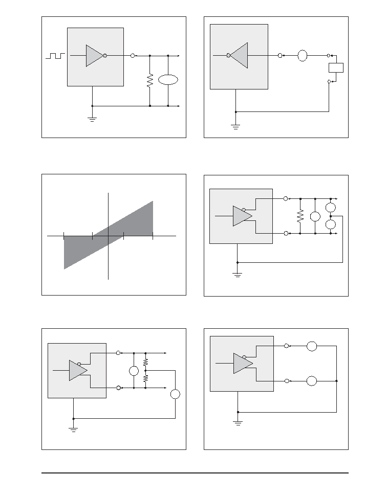
Figure 13. V.10 Driver Output Transition Time
Figure 14. V.10 Receiver Input Current
A
450
C
Oscilloscope
A
C
I
ia
±
10V
+3.25mA
≠3.25mA
+10V
+3V
≠3V
≠10V
Maximum Input Current
versus Voltage
V.10 RECEIVER
Figure 15. V.10 Receiver Input IV Graph
Figure 16. V.11 and V.35 Driver Output Open-Circuit
Voltage
A
B
V
OC
3.9k
V
OCA
V
OCB
C
A
B
V
T
50
V
OS
C
50
A
B
C
I
sa
I
sb
Figure 17. V.11 Driver Output Test Terminated Voltage
Figure 18. V.11 Driver Output Short-Circuit Current

10
Rev: A Date: 1/27/04
SP505 Multi≠Mode Serial Transceiver
© Copyright 2004 Sipex Corporation
A
B
C
I
xa
±
0.25V
A
B
C
I
xb
±
0.25V
V
CC
= 0V
V
CC
= 0V
A
B
C
I
ia
±
10V
C
I
ib
±
10V
A
B
+3.25mA
≠3.25mA
+10V
+3V
≠3V
≠10V
Maximum Input Current
versus Voltage
V.11 RECEIVER
Figure 19. V.11 Driver Output Power-Off Current
Figure 20. V.11 Receiver Input Current
Figure 21. V.11 Driver Output Rise/Fall Time
Figure 22. V.11 Receiver Input IV Graph
A
B
50
C
50
50
V
E
Oscilloscope

11
Rev: A Date: 1/27/04
SP505 Multi≠Mode Serial Transceiver
© Copyright 2004 Sipex Corporation
A
B
C
I
ia
±
6V
C
I
ib
±
6V
A
B
100
to
150
100
to
150
i [mA] = V [V] / 0.1
+6V
+3V
≠3V
≠6V
Maximum Input Current
versus Voltage
V.11 RECEIVER
w/ Optional Cable Termination
(100
to 150
)
i [mA] = V [V] / 0.1
i [mA] = (V [V] ≠ 3) / 4.0
i [mA] = (V [V] ≠ 3) / 4.0
Figure 23. V.11 Receiver Input Current w/ Termination
Figure 24. V.11 Receiver Input Graph w/ Termination
Figure 25. V.35 Driver Output Test Terminated Voltage
Figure 26. V.35 Driver Output Offset Voltage
Figure 27. V.35 Driver Output Source Impedance
A
B
50
C
50
V
T
V
OS
A
B
V
2
50
C
24kHz, 550mV
p-p
Sine Wave
V
1
A
B
50
C
50
V
T
V
OS

12
Rev: A Date: 1/27/04
SP505 Multi≠Mode Serial Transceiver
© Copyright 2004 Sipex Corporation
Figure 32. Driver Output Leakage Current Test
Figure 33. Driver/Receiver Timing Test Circuit
Figure 30. V.35 Receiver Input Source Impedance
Figure 29. V.35 Driver Output Rise/Fall Time
Figure 31. V.35 Receiver Input Short-Circuit Impedance
Figure 28. V.35 Driver Output Short-Circuit Impedance
A
B
C
I
SC
±
2V
A
B
C
50
Oscilloscope
50
50
A
B
C
I
sc
±
2V
C
L1
15pF
R
OUT
A
B
A
B
T
IN
C
L2
f
IN
(50% Duty Cycle, 2.5V
P-P
)
A
B
V
2
50
C
24kHz, 550mV
p-p
Sine Wave
V
1
A
B
I
ZSC
Logic "1"
±
15V
0
0
0
0
DEC
3
DEC
2
DEC
1
DEC
0
V
CC
= +5V
V
CC
Any one of the two conditions for disabling the driver.

13
Rev: A Date: 1/27/04
SP505 Multi≠Mode Serial Transceiver
© Copyright 2004 Sipex Corporation
Figure 34. Driver Timing Test Load Circuit
Figure 35. Receiver Timing Test Load Circuit
500
C
L
Output
Under
Test
S
1
S
2
V
CC
1K
1K
C
RL
Receiver
Output
S
1
S
2
Test Point
V
CC
Figure 36. Driver Propagation Delays
Figure 37. Driver Enable and Disable Times
+3V
0V
DEC
X
5V
V
OL
A, B
0V
1.5V
1.5V
t
ZL
t
ZH
f = 1MHz; t
R
10ns; t
F
10ns
V
OH
A, B
2.3V
2.3V
t
LZ
t
HZ
0.5V
0.5V
Output normally LOW
Output normally HIGH
TX
ENABLE
Figure 38. Receiver Propagation Delays
+3V
0V
DRIVER
INPUT
B
A
DRIVER
OUTPUT
V
O
+
DIFFERENTIAL
OUTPUT
V
A
≠ V
B
0V
V
O
≠
1.5V
1.5V
t
PLH
t
R
t
F
f > 5MHz; t
R
< 10ns; t
F
< 10ns
V
O
1/2V
O
1/2V
O
t
PHL
t
DPLH
t
DPHL
t
SKEW =
|
t
DPLH -
t
DPHL
|
V
OH
V
OL
RECEIVER OUT
(V
OH
- V
OL
)/2
(V
OH
- V
OL
)/2
t
PLH
f > 5MHz; t
R
< 10ns; t
F
< 10ns
OUTPUT
V
0D2
+
V
0D2
≠
A ≠ B
0V
0V
t
PHL
INPUT
t
SKEW
= | t
PHL
- t
PLH
|

14
Rev: A Date: 1/27/04
SP505 Multi≠Mode Serial Transceiver
© Copyright 2004 Sipex Corporation
Figure 39. Receiver Enable and Disable Times
+3V
0V
DEC
X
5V
0V
1.5V
1.5V
t
ZL
t
ZH
f = 1MHz; t
R
10ns; t
F
10ns
RECEIVER OUT
1.5V
1.5V
t
LZ
t
HZ
0.5V
0.5V
Output normally LOW
Output normally HIGH
V
IL
V
IH
RECEIVER OUT
RCVR
ENABLE
+3V
0V
DEC
X
or Tx_Enable
1.5V
1.5V
t
ZL
f = 60kHz; t
R
< 10ns; t
F
< 10ns
T
OUT
t
LZ
Output LOW
0V
+3V
0V
V
OH
1.5V
1.5V
t
ZH
f = 60kHz; t
R
< 10ns; t
F
< 10ns
T
OUT
V
OH
≠ .5V
t
HZ
Output HIGH
0V
DEC
X
or Tx_Enable
V
OH
≠ .5V
V
OL
≠ .5V
V
OL
≠ .5V
V
OL
Figure 40. V.28 (RS-232) and V.10 (RS-423) Driver Enable and Disable Times

15
Rev: A Date: 1/27/04
SP505 Multi≠Mode Serial Transceiver
© Copyright 2004 Sipex Corporation
Figure 41. Typical V.28 Driver Output Waveform
Figure 42. Typical V.10 Driver Output Waveform
- 0V
- 0V
- 0V
- 0V
- 0V
- 0V
- 0V
- 0V
Figure 43. Typical V.11 Driver Output Waveform
Figure 44. Typical V.35 Driver Output Waveform
INPUT
OUTPUT
INPUT
A
OUT
B
OUT
DIFF
OUT

16
Rev: A Date: 1/27/04
SP505 Multi≠Mode Serial Transceiver
© Copyright 2004 Sipex Corporation
PINOUT...
PIN ASSIGNMENTS...
CLOCK AND DATA GROUP
Pin 1 -- RxD -- Receive Data; TTL output,
sourced from RD(a) and RD(b) inputs.
Pin 14 -- TxD -- TTL input ; transmit data
source for SD(a) and SD(b) outputs.
Pin 15 -- TxC -- Transmit Clock; TTL input for
TT driver outputs.
Pin 20 -- RxC -- Receive Clock; TTL output
sourced from RT(a) and RT(b) inputs.
Pin 22 -- ST -- Send Timing; TTL input; source
for ST(a) and ST(b) outputs.
Pin 37 -- RT(a) -- Receive Timing; analog
input, inverted; source for RxC.
Pin 38 -- RT(b) -- Receive Timing; analog
input, non-inverted; source for RxC.
Pin 42 -- ST(a) -- Send Timing; analog output,
inverted; sourced from ST.
Pin 44 -- ST(b) -- Send Timing; analog output,
non-inverted; sourced from ST.
Pin 59 -- SD(b) -- Analog Out -- Send data,
non-inverted; sourced from TxD.
Pin 61 -- SD(a) -- Analog Out -- Send data,
inverted; sourced from TxD.
Pin 63 -- TT(a) -- Analog Out -- Terminal
Timing, inverted; sourced from TxC
Pin 65 -- TT(b) -- Analog Out -- Terminal
Timing, non≠inverted; sourced from TxC.
Pin 70 -- RD(a) -- Receive Data, analog input;
inverted; source for RxD.
Pin 71 -- RD(b) -- Receive Data; analog input;
non-inverted; source for RxD.
Pin 76 -- SCT(a) -- Serial Clock Transmit;
analog input, inverted; source for SCT.
Pin 77 -- SCT(b) -- Serial Clock Transmit:
analog input, non≠inverted; source for SCT
Pin 79 -- SCT -- Serial Clock Transmit; TTL
output; sources from SCT(a) and SCT(b) inputs.
CONTROL LINE GROUP
Pin 13 -- DTR -- Data Terminal Ready; TTL
input; source for TR(a) and TR(b) outputs.
Pin 16 -- RTS -- Ready To Send; TTL input;
source for RS(a) and RS(b) outputs.
Pin 17 -- RL -- Remote Loopback; TTL input;
source for RL(a) and RL(b) outputs.
Pin 19 -- DCD-- Data Carrier Detect; TTL
output; sourced from RR(a) and RR(b) inputs.
Pin 21 -- RI -- Ring In; TTL output; sourced
from IC(a) and IC(b) inputs.
Pin 24 -- LL -- Local Loopback; TTL input;
source for LL(a) and LL(b) outputs.
Pin 35 -- RR(a)-- Receiver Ready; analog
input, inverted; source for DCD.
Pin 36 -- RR(b)-- Receiver Ready; analog
input, non-inverted; source for DCD.
Pin 39 -- IC(a)-- Incoming Call; analog input,
inverted; source for RI.
Pin 40 -- IC(b)-- Incoming Call; analog
input,non-inverted; source for RI.
RxD 1
SDEN
2
TREN
3
RSEN 4
LLEN
5
TTEN 6
SCTEN 7
LATCH 8
DEC
3
9
DEC
2
10
DEC
1
11
DEC
0
12
DTR 13
TxD 14
TxC 15
RTS 16
RL 17
RLEN 18
DCD 19
RxC 20
RI 21
ST 22
STEN 23
LL 24
V
CC
25
C
1
+
26
V
DD
27
C
2
+
28
GND 29
C
1
≠
30
C
2
≠
31
V
SS
32
V
CC
33
GND 34
RR(a) 35
RR(b) 36
R
T(a) 37
R
T(b) 38
IC(a) 39
IC(b) 40
60 GND
59 SD(b)
58 TR(a)
57 GND
56 TR(b)
55 V
CC
54 RS(a)
53 GND
52 RS(b)
51 LL(a)
50 GND
49 LL(b)
48 V
CC
47 RL(a)
46 GND
45 RL(b)
44 ST(b)
43 GND
42 ST(a)
41 V
CC
80 CTS
79 SCT
78 DSR
77 SCT(b)
76 SCT(a)
75 GND
74
V
CC
73
V
CC
72 GND
71 RD(b)
70 RD(a)
69 DM(b)
68 DM(a)
67 CS(b)
66 CS(a)
65
TT(b)
64 GND
63
TT(a)
62
V
CC
61 SD(a)
SP505

17
Rev: A Date: 1/27/04
SP505 Multi≠Mode Serial Transceiver
© Copyright 2004 Sipex Corporation
Pin 7 -- SCTEN -- Enables SCT receiver;
active high; TTL input.
Pin 8 -- LATCH -- Latch control for decoder
bits (pins 9-12), active low. Logic high input
will make decoder transparent.
Pins 12≠9 -- DEC
0
≠ DEC
3
-- Transmitter and
receiver decode register; configures transmitter
and receiver modes; TTL inputs.
Pin 18 -- RLEN -- Enables RL driver; active
low; TTL input.
Pin 23 -- STEN -- Enables ST driver; active
low; TTL input.
POWER SUPPLIES
Pins 25, 33, 41, 48, 55, 62, 73, 74 -- V
CC
-- +5V
input.
Pins 29, 34, 43, 46, 50, 53, 57, 60, 64, 72, 75 --
GND -- Ground.
Pin 27 -- V
DD
+10V Charge Pump Capacitor --
Connects from V
DD
to V
CC
. Suggested capaci-
tor size is 22
µF, 16V.
Pin 32 -- V
SS
≠10V Charge Pump Capacitor --
Connects from ground to V
SS
. Suggested ca-
pacitor size is 22
µF, 16V.
Pins 26 and 30 -- C
1
+
and C
1
≠
-- Charge Pump
Capacitor -- Connects from C
1
+
to C
1
≠
. Sug-
gested capacitor size is 22
µF, 16V.
Pins 28 and 31 -- C
2
+
and C
2
≠
-- Charge Pump
Capacitor -- Connects from C
2
+
to C
2
≠
. Sug-
gested capacitor size is 22
µF, 16V.
Pin 45 -- RL(b) -- Remote Loopback; analog
output, non-inverted; sourced from RL.
Pin 47 -- RL(a) -- Remote Loopback; analog
output inverted; sourced from RL.
Pin 49-- LL(b) -- Local Loopback; analog
output, non-inverted; sourced from LL.
Pin 51 -- LL(a) -- Local Loopback; analog
output, inverted; sourced from LL.
Pin 52 -- RS(b) -- Ready To Send; analog
output, non-inverted; sourced from RTS.
Pin 54 -- RS(a) -- Ready To Send; analog
output, inverted; sourced from RTS.
Pin 56 -- TR(b) -- Terminal Ready; analog
output, non-inverted; sourced from DTR.
Pin 58 -- TR(a) -- Terminal Ready; analog
output, inverted; sourced from DTR.
Pin 66 -- CS(a)-- Clear To Send; analog input,
inverted; source for CTS.
Pin 67 -- CS(b)-- Clear To Send; analog input,
non-inverted; source for CTS.
Pin 68 -- DM(a)-- Data Mode; analog input,
inverted; source for DSR.
Pin 69 -- DM(b)-- Data Mode; analog input,
non-inverted; source for DSR
Pin 78 -- DSR-- Data Set Ready; TTL output;
sourced from DM(a), DM(b) inputs.
Pin 80 -- CTS-- Clear To Send; TTL output;
sourced from CS(a) and CS(b) inputs.
CONTROL REGISTERS
Pins 2 -- SDEN -- Enables TxD driver, active
low; TTL input.
Pins 3 -- TREN -- Enables DTR driver, active
low; TTL input.
Pins 4 -- RSEN -- Enables RTS driver, active
low; TTL input.
Pins 5 -- LLEN -- Enables LL driver, active
low; TTL input.
Pin 6 -- TTEN -- Enables TT driver, active
low; TTL input.

18
Rev: A Date: 1/27/04
SP505 Multi≠Mode Serial Transceiver
© Copyright 2004 Sipex Corporation
A typical +10V charge pump would require
external clamping such as 5V zener diodes on
V
DD
and V
SS
to ground. The +5V output has
symmetrical levels as in the +10V output. The
+5V is used in the following modes where RS-
423 (V.10) are used: RS-449, EIA-530, EIA-
530A and V.36.
Phase 1 (±10V)
-- V
SS
charge storage -- During this phase of
the clock cycle, the positive side of capacitors
C
1
and C
2
are initially charged to +5V. C
l
+
is
then switched to ground and the charge on C
1
≠
is
transferred to C
2
≠
. Since C
2
+
is connected to
+5V, the voltage potential across capacitor C
2
is
now 10V.
Phase 1 (±5V)
-- V
SS
& V
DD
charge storage and transfer --
With the C
1
and C
2
capacitors initially charged
to +5V, C
l
+
is then switched to ground and the
charge on C
1
≠
is transferred to the V
SS
storage
capacitor. Simultaneously the C
2
≠
is switched to
ground and 5V charge on C
2
+
is transferred to
the V
DD
storage capacitor.
FEATURES...
The SP505 is a highly integrated serial trans-
ceiver that allows software control of its inter-
face modes. Similar to the SP504, the SP505
offers the same hardware interface modes for
RS-232 (V.28), RS-422A (V.11), RS-449, RS-
485, V.35, EIA-530 and includes V.36 and EIA-
530A. The interface mode selection is done via
a 4≠bit switch for the drivers and receivers. The
SP505 is fabricated using low≠power BiCMOS
process technology, and incorporates a Sipex≠
patented (5,306,954) charge pump allowing +5V
only operation. Each device is packaged in an
80≠pin JEDEC Quad FlatPack package.
The SP505 is ideally suited for wide area net-
work connectivity based on the interface modes
offered and the driver and receiver configura-
tions. The SP505 has seven (7) independent
drivers and seven (7) independent receivers. In
V.35 mode, the SP505 includes the necessary
components and termination resistors internal
within the device for compliant V.35 operation.
THEORY OF OPERATION
The SP505 is made up of five separate circuit
blocks -- the charge pump, drivers, receivers,
decoder and switching array. Each of these
circuit blocks is described in more detail below.
Charge≠Pump
The SP505 charge pump is based on the SP504
design where Sipex's patented charge pump
design (5,306,954) uses a four≠phase voltage
shifting technique to attain symmetrical 10V
power supplies. The charge pump still requires
external capacitors to store the charge. In addi-
tion the SP504 charge pump supplies +10V or
+5V on V
SS
and V
DD
depending on the mode of
operation. There is a free≠running oscillator
that controls the four phases of the voltage
shifting. A description of each phase follows.
The SP505 charge pump is used for RS-232
where the output voltage swing is typically
+10V and also used for RS-423. However, RS-
423 requires the voltage swing on the driver
output be between +4V to +6V during an open-
circuit (no load). The charge pump would need
to be regulated down from +10V to +5V.
V
CC
= +5V
≠5V
≠5V
+5V
V
DD
Storage Capacitor
C
1
C
2
C
4
+
+
+
≠
≠
≠
V
SS
Storage Capacitor
C
3
+
≠
Figure 46. Charge Pump Phase 1 for +5V.
V
CC
= +5V
+5V
V
DD
Storage Capacitor
C
1
C
2
C
4
+
+
+
≠
≠
≠
V
SS
Storage Capacitor
C
3
+
≠
≠5V
Figure 45. Charge Pump Phase 1 for +10V.

19
Rev: A Date: 1/27/04
SP505 Multi≠Mode Serial Transceiver
© Copyright 2004 Sipex Corporation
Phase 2 (±10V)
-- V
SS
transfer -- Phase two of the clock con-
nects the negative terminal of C
2
to the V
SS
storage capacitor and the positive terminal of C
2
to ground, and transfers the generated ≠l0V or
the generated ≠5V to C
3
. Simultaneously, the
positive side of capacitor C
1
is switched to +5V
and the negative side is connected to ground.
Phase 2 (±5V)
-- V
SS
& V
DD
charge storage -- C
1
+
is recon-
nected to V
CC
to recharge the C
1
capacitor. C
2
+
is switched to ground and C
2
≠
is connected to C
3
.
The 5V charge from Phase 1 is now transferred
to the V
SS
storage capacitor. V
SS
receives a
continuous charge from either C
1
or C
2
. With
the C1 capacitor charged to 5V, the cycle begins
again.
Phase 3
-- V
DD
charge storage -- The third phase of the
clock is identical to the first phase -- the charge
transferred in C
1
produces ≠5V in the negative
terminal of C
1
, which is applied to the negative
side of capacitor C
2
. Since C
2
+
is at +5V, the
voltage potential across C
2
is l0V. For the 5V
output, C
2
+
is connected to ground so that the
potential on C
2
is only +5V.
Phase 4
-- V
DD
transfer -- The fourth phase of the
clock connects the negative terminal of C
2
to
ground and transfers the generated l0V or the
generated 5V across C
2
to C
4
, the V
DD
storage
capacitor. Again, simultaneously with this, the
positive side of capacitor C
1
is switched to +5V
and the negative side is connected to ground,
and the cycle begins again.
Since both V
DD
and V
SS
are separately gener-
ated from V
CC
in a no≠load condition, V
DD
and
V
SS
will be symmetrical. Older charge pump
approaches that generate V
≠
from V
+
will show
a decrease in the magnitude of V
≠
compared to
V
+
due to the inherent inefficiencies in the
design.
The clock rate for the charge pump typically
operates at 15kHz. The external capacitors must
be a minimum of 22
µF with a 16V breakdown
rating.
External Power Supplies
For applications that do not require +5V only,
external supplies can be applied at the V+ and
V
≠
pins. The value of the external supply volt-
ages must be no greater than +l0.5V. The toler-
ance should be +5% from +10V. The current
drain for the supplies is used for RS-232 and RS-
423 drivers. For the RS-232 driver, the current
requirement will be 3.5mA per driver. The RS-
423 driver worst case current drain will be
11mA per driver. Power sequencing is required
for the SP505. The supplies must be sequenced
accordingly: +10V, +5V and ≠10V. It is impor-
tant to prevent V
SS
from starting up before V
CC
or V
DD
.
Figure 47. Charge Pump Phase 2 for +10V.
Figure 49. Charge Pump Phase 3.
V
CC
= +5V
≠10V
V
DD
Storage Capacitor
C
1
C
2
C
4
+
+
+
≠
≠
≠
V
SS
Storage Capacitor
C
3
+
≠
V
CC
= +5V
≠5V
≠5V
+5V
V
DD
Storage Capacitor
C
1
C
2
C
4
+
+
+
≠
≠
≠
V
SS
Storage Capacitor
C
3
+
≠
Figure 50. Charge Pump Phase 4.
Figure 48. Charge Pump Phase 2 for +5V.
V
CC
= +5V
V
DD
Storage Capacitor
C
1
C
2
C
4
+
+
+
≠
≠
≠
V
SS
Storage Capacitor
C
3
+
≠
≠5V
V
CC
= +5V
+10V
V
DD
Storage Capacitor
C
1
C
2
C
4
+
+
+
≠
≠
≠
V
SS
Storage Capacitor
C
3
+
≠

20
Rev: A Date: 1/27/04
SP505 Multi≠Mode Serial Transceiver
© Copyright 2004 Sipex Corporation
requirements of ±1.5V minimum differential
output levels with a 54
load. The driver is
designed to operate over a common mode range
of +12V to -7V, which follows the RS-485
specification. This also covers the +7V to -7V
common mode range for V.11 (RS-422) re-
quirements. The V.11 drivers are used in RS-
449, EIA-530, EIA-530A and V.36 modes as
Category I signals which are used for clock and
data signals.
V.35 Drivers
The fourth type of driver is the V.35 driver.
These drivers were specifically designed to com-
ply with the requirements of V.35. Unique to
the industry, the Sipex's V.35 driver architec-
ture used in the SP505 does not need external
termination resistors to operate and comply with
V.35. This simplifies existing V.35 implemen-
tations that use external termination schemes.
The V.35 drivers can produce +0.55V driver
output signals with minimum deviation (maxi-
mum 20%) given an equivalent load of 100
.
With the help of internal resistor networks, the
drivers achieve the 50
to 150 source imped-
ance and the 135
to 165 short-circuit imped-
ance for V.35. The V.35 driver is disabled and
transparent when the decoder is in all other
modes. All of the differential drivers; V.11 (RS-
422) and V.35, can operate over 10Mbps.
Driver Enable and Input
All the drivers in the SP505 contain individual
enable lines which can tri-state the driver out-
puts when a logic "1" is applied. This simplifies
half-duplex configurations for some applica-
tions and also provides simpler DTE/DCE
flexibility with one integrated circuit.
The driver inputs are both TTL or CMOS
compatible. Each driver input should have a
pull-down or pull-up resistor so that the output
will be at a defined state. Unused driver inputs
should not be left floating.
Receivers
The SP505 has seven (7) independent receivers
which can be programmed for the different
interface modes. Control for the mode selection
is done via a 4≠bit control word, which is the
same as the driver's 4-bit control word.
Like the drivers, the receivers are prearranged
for the specific requirements of the synchronous
Drivers
The SP505 has seven (7) enhanced independent
drivers. Control for the mode selection is done
via a four≠bit control word. The drivers are
prearranged such that for each mode of opera-
tion, the relative position and functionality of
the drivers are set up to accommodate the se-
lected interface mode. As the mode of the driv-
ers is changed, the electrical characteristics will
change to support the requirements of clock,
data, and control line signal levels. Table 1
shows the mode of each driver in the different
interface modes that can be selected.
There are four basic types of driver circuits --
V.28, V.11, V.10 and V.35.
V.28 Drivers
The V.28 drivers output single≠ended signals
with a minimum of +5V (with 3k
& 2500pF
loading), and can operate to at least 120kbps
under full load. Since the SP505 uses a charge
pump to generate the RS-232 output rails, the
driver outputs will never exceed +10V. The
V.28 drivers are used in RS-232 mode for all
signals, and also in V.35 mode where four (4)
drivers are used as the control line signals (DTR,
RTS, LL, and RL).
V.10 Drivers
The V.10 (RS-423) drivers are also single≠
ended signals which produce open circuit V
OL
and V
OH
measurements of +4.0V to +6.0V.
When terminated with a 450
load to ground,
the driver output will not deviate more than 10%
of the open circuit value. This is in compliance
of the ITU V.10 specification. The V.10 drivers
are used in RS-449, EIA-530, EIA-530A and
V.36 modes as Category II signals from each of
their corresponding specifications.
V.11 Drivers
The third type of driver is a V.11 (RS-422) type
differential driver. Due to the nature of differ-
ential signaling, the drivers are more immune to
noise as opposed to single-ended transmission
methods. The advantage is evident over high
speeds and long transmission lines. The strength
of the driver outputs can produce differential
signals that can maintain typically +2.2V differ-
ential output levels with a load of 100
. The
signal levels and drive capability of these driv-
ers allow the drivers to also support RS-485

21
Rev: A Date: 1/27/04
SP505 Multi≠Mode Serial Transceiver
© Copyright 2004 Sipex Corporation
serial interface. As the operating mode of the
receivers is changed, the electrical characteris-
tics will change to support the requirements of
clock, data, and control line receivers. Table 2
shows the mode of each receiver in the different
interface modes that can be selected.
There are three basic types of receiver circuits
-- V.28, V.10, and V.11.
V.28 Receivers
The V.28 receiver is single≠ended and accepts
V.28 signals from the V.28 driver. The V.28
receiver has an operating voltage range of +15V
and can receive signals down to +3V. The input
sensitivity complies with RS-232 and V.28 speci-
fications at +3V. The input impedance is 3k
to
7k
in accordance to RS-232 and V.28 over a
+15V input range. The receiver output pro-
duces a TTL/CMOS signal with a +2.4V mini-
mum for a logic "1" and a +0.8V maximum for
a logic "0". V.28 receivers are used in RS-232
mode for all data, clock and control signals.
They are also used in V.35 mode for control line
signals: CTS, DSR, LL, and RL. The V.28
receivers can operate to at least 120kbps.
V.10 Receivers
The V.10 receivers are also single≠ended as
with the V.28 receivers but have an input thresh-
old as low as +200mV. The input impedance is
guaranteed to be greater than 4K
, with an
operating voltage range of +7V. The V.10 re-
ceivers can operate to at least 120kbps. V.10
receivers are used in RS-449, EIA-530, EIA-
530A and V.36 modes as Category II signals as
indicated by their corresponding specifications.
V.11 Receivers
The third type of receiver is a differential which
supports V.11 and RS-485 signals. This re-
ceiver has a typical input impedance of 10k
and a typical differential threshold of +200mV,
which complies with the V.11 specification.
Since the characteristics of the V.11 receivers
are actually subsets of RS-485, the V.11 receiv-
ers can accept RS-485 signals. However, these
receivers cannot support 32-transceivers on the
signal bus due to the lower input impedance as
specified in the RS-485 specification. Three
receivers (RxD, RxC, and SCT) include a typi-
cal 120
cable termination resistor across the A
and B inputs. The resistor for the three receivers
is switched on when the SP505 is configured in
a mode which uses V.11 receivers. The V.11
cable termination resistor is switched off when
the receiver is disabled or in another operating
mode not using V.11 receivers. The V.11 re-
ceivers are used in X.21, RS-449, EIA-530,
EIA-530A and V.36 as Category I signals for
receiving clock, data, and some control line
signals not covered by Category II V.10 circuits.
The differential receivers can receive signals
over 10Mbps.
V.35 Receiver
The V.11 receivers are also used for the V.35
mode. Unlike the older implementations of
differential receivers used for V.35, the SP505
contains an internal resistor termination net-
work that ensures a V.35 input impedance of
100
(+10) and a short-circuit impedance of
150
(+15). The traditional V.35 implemen-
tations required external termination resistors to
achieve the proper V.35 impedances. The inter-
nal network is connected via low on-resistance
FET switches when the decoder is changed to
V.35 mode. These FET switches can accept
input signals of up to +15V without any forward
biasing and other parasitic affects. The V.35
termination resistor network is switched off
when the receiver is disabled either by the de-
coder or receiver enable pin. The termination
network is transparent when all other modes are
selected. The V.35 receivers can operate over
10Mbps.
Receiver Enable and Output
Only one receiver includes an enable line. The
SCTEN input for the SCT receiver can enable or
tri-state the output of the receiver. When the pin
is at a logic "0", the receiver output is high
impedance and any input termination internal
connected is switched off. The inputs will be at
approximately 10k
during tri-state.
V.11 TERMINATION
MODE [0100]
V.35 MODE
R
IN
[a]
R
IN
[b]
To Non-Inverting
Input of Receiver
To Inverting Input
of Receiver
r
ON
= 20
r
ON
= 1
51
51
124
r
ON
= 1
Figure 51. Simplified R
IN
Termination Circuit

22
Rev: A Date: 1/27/04
SP505 Multi≠Mode Serial Transceiver
© Copyright 2004 Sipex Corporation
All receivers include a fail-safe feature that
outputs a logic "1" when the receiver inputs are
open. The differential receivers allocated for
data and clock signals (RxD, RxC, and SCT)
have advanced fail-safe that outputs a logic "1"
when the inputs are either open, shorted, or
terminated. Other discrete or integrated imple-
mentations require external pull-up and pull-
down resistors to define the receiver output
state. For single-ended V.28 receivers, there are
internal 5k
pull-down resistors on the inputs
which produces a logic high ("1") at the receiver
outputs. The single-ended V.10 receivers pro-
duce a logic LOW ("0") on the output when the
inputs are open. This is due to an internal pull-
up device connected to the input. The differen-
tial receivers have the same internal pull-up
device on the non-inverting input which pro-
duces a logic HIGH ("1") at the receiver output,
representing an "OFF" state to the HDLC con-
troller. The three differential receivers when
configured in V.35 mode (RxD, RxC & SCT)
will also include fail-safe even when the internal
termination resistor network is connected and
the inputs are either shorted or floating.
Decoder
The SP505 has the ability to change the inter-
face mode of the drivers or receivers via a 4≠bit
switch. The decoder for the drivers and receiv-
ers can be latched through a control pin.
The control word can be latched either high or
low to write the appropriate code into the SP505.
The codes shown in Tables 1 and 2 are the only
specified, valid modes for the SP505. Unde-
fined codes may represent other interface modes
not specified (consult the factory for more infor-
mation). The drivers and receivers are con-
trolled with the data bits labeled DEC
3
≠DEC
0
.
All of the drivers outputs and receiver outputs
can be put into tri-state mode by writing 0000 to
the driver decode switch. All internal termina-
tion networks are switched off during this mode.
Individual tri-state capability is possible for all
drivers through each driver's own enable control
input. The SCT receiver also contains an indi-
vidual enable input. When this control pin is
disabled (logic "0"), the V.11 and V.35 input
termination is deactivated. The 0000 decoder
word will override the enable control line for the
one receiver (SCT).
The SP505 contains internal loopback capabili-
ties for self-diagnostic tests. Loopback is en-
abled through the decoder. To initiate single-
ended mode loopback, the decoder word is 1010.
To initiate differential mode loopback, the de-
coder word is 1011. The minimum transmission
rates into the SP505 under loopback conditions
are 120kbps for single-ended mode and 5Mbps
for differential mode. The driver outputs are tri-
stated and the receiver inputs are disabled dur-
ing loopback. The receiver input impedance
during loopback is approximately 10k
.
The SP505 is equipped with a latch control for
the four (4) decoder bits. The latch control pin
is pin 8 of the SP505. The latch control is active
low, a logic low on pin 8 will latch the decoder
signals. A logic "1" on pin 8 will force the latch
to be transparent to the user. A pulse width of at
least 30ns is required to latch the decoder for the
next mode. The resultant output is typically
600ns after the latch control pin is toggled
assuming that the decoder word is set.
NET1/2 & TBR2 European Compliancy
As with all of Sipex's previous multi-protocol
serial transceiver ICs, the drivers and receivers
have been designed to meet all the requirements
to NET1/2. The SP505 is internally tested to all
the NET1/2 physical layer testing parameters
and the ITU Series V specifications.
With the emergence of ETSI TBR2 (Technical
Basis for Regulation) document now in place as
an alternative for European compliancy, Sipex
has tested the SP505 to TBR2 specifications to
ensure "CE" approval for either testing method.
The SP505 was externally tested by TUV
Telecom Services, Division of TUV Rheinland,
and passed both NET1/2 and TBR2 require-
ments. Test reports
(NET2/052101/98 for NET1/2 and CTR2/
05101/98 for TBR2)
can be furnished upon request.
Please note that although the SP505 adheres to
NET1/2 testing; any complex or unusual con-
figuration should be double-checked to ensure
NET compliance. Consult factory for details.
23
Rev: A Date: 1/27/04
SP505 Multi≠Mode Serial Transceiver
© Copyright 2004 Sipex Corporation
SP505 Receiver Mode Selection
SP505 Driver Mode Selection
Pin Label
RD(a)
RD(b)
RT(a)
RT(b)
CS(a)
CS(b)
DM(a)
DM(b)
RR(a)
RR(b)
IC(a)
IC(b)
SCT(a)
SCT(b)
Pin Label
Mode:
RS232
V.35
RS422
RS449
EIA530
EIA-530A
V.36
0000
0010
1110
0100
0101
1100
1101
1111
0110
SD(a)
tri-state
V.28
V.35≠
V.11≠
V.11≠
V.11≠
SD(b)
V.35+
V.11+
V.11+
V.11+
TR(a)
tri-state
V.28
V.11≠
V.11≠
V.11≠
V.10
TR(b)
tri-state
tri-state
tri-state
V.11+
V.11+
V.11+
tri-state
RS(a)
tri-state
V.28
V.11≠
V.11≠
V.11≠
RS(b)
tri-state
tri-state
tri-state
V.11+
V.11+
V.11+
RL(a)
tri-state
V.28
V.11≠
V.11≠
V.10
RL(b)
tri-state
tri-state
tri-state
V.11+
V.11+
tri-state
LL(a)
tri-state
V.28
V.11≠
V.11≠
V.10
LL(b)
tri-state
tri-state
tri-state
V.11+
V.11+
tri-state
ST(a)
tri-state
V.28
V.35≠
V.11≠
V.11≠
V.11≠
ST(b)
V.35+
V.11+
V.11+
V.11+
TT(a)
tri-state
V.28
V.35≠
V.11≠
V.11≠
V.11≠
TT(b)
V.35+
V.11+
V.11+
V.11+
tri-state
tri-state
tri-state
tri-state
tri-state
tri-state
V.28
V.28
V.28
V.28
V.11≠
V.11+
V.11≠
V.11+
V.11≠
V.11+
tri-state
V.11≠
V.11+
V.11≠
V.11+
V.10
V.11≠
V.11+
V.11≠
V.11+
V.11≠
V.11+
V.11≠
V.11+
V.11≠
V.11+
V.10
tri-state
V.10
tri-state
V.11≠
V.11+
V.10
tri-state
V.10
tri-state
V.10
tri-state
V.11≠
V.11+
V.11≠
V.11+
Mode:
RS232
V.35
RS422
w/ Term.
RS422
RS449
EIA530
EIA-530A
V.36
0000
0010
1110
0100
0101
1100
1101
1111
0110
V.28
V.35≠
V.11≠
V.11≠
V.11≠
V.35+
V.11+
V.11+
V.11+
V.28
V.11≠
V.11≠
V.11≠
V.11+
V.11+
V.11+
V.28
V.11≠
V.11≠
V.11≠
V.11+
V.11+
V.11+
V.28
V.11≠
V.11≠
V.11+
V.11+
V.28
V.11≠
V.11≠
V.11+
V.11+
V.28
V.11≠
V.11≠
V.11+
V.11+
V.28
V.35≠
V.11≠
V.11≠
V.11≠
V.35+
V.11+
V.11+
V.11+
V.28
V.28
V.28
V.11≠
V.11+
V.11≠
V.11+
V.11≠
V.11+
V.10
V.10
V.10
>10k
to GND
>10k
to GND
>10k
to GND
>10k
to GND
>10k
to GND
>10k
to GND
>10k
to GND
>10k
to GND
>10k
to GND
>10k
to GND
>10k
to GND
>10k
to GND
>10k
to GND
>10k
to GND
>10k
to GND
>10k
to GND
>10k
to GND >12k
to GND
>10k
to GND
>10k
to GND
>10k
to GND
>10k
to GND
>10k
to GND
>10k
to GND
>10k
to GND
>10k
to GND
>10k
to GND
V.11≠
V.11+
V.11≠
V.11+
>10k
to GND
>10k
to GND
V.10
V.10
>10k
to GND
V.10
>10k
to GND
V.10
V.11≠
V.11+
V.11≠
V.11+
V.11≠
V.11+
>10k
to GND
V.10
V.35≠
V.35+
V.28
>10k
to GND
V.11≠
V.11+
3
0
DEC ≠ DEC
3
0
DEC ≠ DEC
120
120
120
RS422
w/ Term.
120
120
120
V.11≠
V.11+
V.11≠
V.11+
120
120
120
V.11≠
V.11+
V.11≠
V.11+
V.11≠
V.11+
120
120
120
V.11≠
V.11+
V.11≠
V.11+
V.11≠
V.11+
120
120
120
Table 1. SP505 Driver Decoder Table
Table 2. SP505 Receiver Decoder Table

24
Rev: A Date: 1/27/04
SP505 Multi≠Mode Serial Transceiver
© Copyright 2004 Sipex Corporation
Figure 52. SP505 Typical Operating Circuit
RD(a) 70
RxD 1
RD(b) 71
RT(a) 37
RxC 20
RT(b) 38
CS(a) 66
CTS 80
CS(b) 67
DM(a) 68
DSR 78
DM (b) 69
RR(a) 35
DCD 19
RR(b) 36
IC(a) 39
RI 21
IC(b) 40
SCT(a) 76
SCT 79
SCTEN 7
SCT(b) 77
14 TxD
61 SD(a)
59 SD(b)
2 SDEN
22 ST
42 ST(a)
44 ST(b)
23 STEN
15 TxC
63 TT(a)
65 TT(b)
6 TTEN
13 DTR
58 TR(a)
56 TR(b)
3 TREN
16 RTS
54 RS(a)
52 RS(b)
4 RSEN
17 RL
47 RL(a)
45 RL(b)
18 RLEN
24 LL
51 LL(a)
49 LL(b)
5 LLEN
22
µ
F
22
µ
F
1N5819
VCC
VDD
C1-
C2-
VSS
C1+
C2+
22
µ
F
+5V
10
µ
F
27
25
26
31
28
30
22
µ
F
32
9
10
11
12
MODE
X
0
1
0
0
RS-422 Mode
Input Word
A
B
Charge Pump
A -- Receiver Tri-State circuitry,
V.11, & V.35 termination
resistor circuitry (RxD,
RxC & SCT).
B -- Driver Tri-State circuitry &
V.35 termination circuitry
(TxD, TxC & ST).
SP505
(SEE PINOUT ASSIGNMENTS FOR GROUND PINS)
8
DECODER LA
TCH
LATCH
(SEE PINOUT FOR V
CC
PINS)

25
Rev: A Date: 1/27/04
SP505 Multi≠Mode Serial Transceiver
© Copyright 2004 Sipex Corporation
Figure 53. Mode Diagram -- RS-232
MODE: RS-232 (V.28)
DRIVER/RECEIVER
DEC
3
DEC
2
DEC
1
DEC
0
IC(a) 39
RI 21
SCTEN 7
RECEIVERS DRIVERS
0 0 1 0
24 LL
51 LL(a)
5 LLEN
13 DTR
58 TR(a)
3 TREN
DM(a) 68
DSR 78
16 RTS
54 RS(a)
4 RSEN
17 RL
47 RL(a)
18 RLEN
RR(a) 35
DCD 19
CS(a) 66
CTS 80
RD(a) 70
RxD 1
RT(a) 37
RxC 20
SCT(a) 76
SCT 79
14 TxD
61 SD(a)
2 SDEN
15 TxC
63 TT(a)
6 TTEN
22 ST
42 ST(a)
23 STEN

26
Rev: A Date: 1/27/04
SP505 Multi≠Mode Serial Transceiver
© Copyright 2004 Sipex Corporation
Figure 54. Mode Diagram -- V.35
MODE: V.35
DRIVER/RECEIVER
DEC
3
DEC
2
DEC
1
DEC
0
RD(a) 70
RxD 1
RT(a) 37
RxC 20
IC(a) 39
RI 21
SCT(a) 76
SCT 79
SCTEN 7
SCT(b) 77
15 TxC
63 TT(a)
65 TT(b)
6 TTEN
RECEIVERS DRIVERS
22 ST
42 ST(a)
44 ST(b)
23 STEN
RT(b) 38
RD(b) 71
1 1 1 0
24 LL
51 LL(a)
5 LLEN
14 TxD
61 SD(a)
59 SD(b)
2 SDEN
13 DTR
58 TR(a)
3 TREN
DM(a) 68
DSR 78
16 RTS
54 RS(a)
4 RSEN
17 RL
47 RL(a)
18 RLEN
RR(a) 35
DCD 19
CS(a) 66
CTS 80
V
.35 Ntwk
V
.35 Ntwk
V
.35 Ntwk
V
.35 Ntwk
V
.35 Ntwk
V
.35 Ntwk

27
Rev: A Date: 1/27/04
SP505 Multi≠Mode Serial Transceiver
© Copyright 2004 Sipex Corporation
Figure 55. Mode Diagram -- RS-422
MODE: RS-422
[w/ termination]
DRIVER/RECEIVER
DEC
3
DEC
2
DEC
1
DEC
0
RD(a) 70
RxD 1
RT(a) 37
RxC 20
SCT(a) 76
SCT 79
SCTEN 7
SCT(b) 77
15 TxC
63 TT(a)
65 TT(b)
6 TTEN
RECEIVERS DRIVERS
22 ST
42 ST(a)
44 ST(b)
23 STEN
CS(a) 66
CTS 80
RR(a) 35
DCD 19
RR(b) 36
CS(b) 67
RT(b) 38
RD(b) 71
0 1 0 0
24 LL
51 LL(a)
49 LL(b)
5 LLEN
14 TxD
61 SD(a)
59 SD(b)
2 SDEN
13 DTR
58 TR(a)
56 TR(b)
3 TREN
16 RTS
54 RS(a)
52 RS(b)
4 RSEN
17 RL
47 RL(a)
45 RL(b)
18 RLEN
IC(a) 39
RI 21
IC(b) 40
DM(a) 68
DSR 78
DM(b) 69
120
120
120

28
Rev: A Date: 1/27/04
SP505 Multi≠Mode Serial Transceiver
© Copyright 2004 Sipex Corporation
Figure 56. Mode Diagram -- RS-449
MODE: RS-449
DRIVER/RECEIVER
DEC
3
DEC
2
DEC
1
DEC
0
RD(a) 70
RxD 1
RT(a) 37
RxC 20
IC(a) 39
RI 21
SCT(a) 76
SCT 79
SCTEN 7
SCT(b) 77
15 TxC
63 TT(a)
65 TT(b)
6 TTEN
RECEIVERS DRIVERS
22 ST
42 ST(a)
44 ST(b)
23 STEN
CS(a) 66
CTS 80
RR(a) 35
DCD 19
RR(b) 36
CS(b) 67
RT(b) 38
RD(b) 71
1 1 0 0
24 LL
51 LL(a)
5 LLEN
14 TxD
61 SD(a)
59 SD(b)
2 SDEN
13 DTR
58 TR(a)
56 TR(b)
3 TREN
16 RTS
54 RS(a)
52 RS(b)
4 RSEN
DM(a) 68
DSR 78
DM(b) 69
17 RL
47 RL(a)
18 RLEN
120
120
120

29
Rev: A Date: 1/27/04
SP505 Multi≠Mode Serial Transceiver
© Copyright 2004 Sipex Corporation
Figure 57. Mode Diagram -- RS-422 w/o termination
MODE: RS-422
[no termination]
DRIVER/RECEIVER
DEC
3
DEC
2
DEC
1
DEC
0
RD(a) 70
RxD 1
RT(a) 37
RxC 20
SCT(a) 76
SCT 79
SCTEN 7
SCT(b) 77
15 TxC
63 TT(a)
65 TT(b)
6 TTEN
RECEIVERS DRIVERS
22 ST
42 ST(a)
44 ST(b)
23 STEN
CS(a) 66
CTS 80
RR(a) 35
DCD 19
RR(b) 36
CS(b) 67
RT(b) 38
RD(b) 71
0 1 0 1
24 LL
51 LL(a)
49 LL(b)
5 LLEN
14 TxD
61 SD(a)
59 SD(b)
2 SDEN
13 DTR
58 TR(a)
56 TR(b)
3 TREN
16 RTS
54 RS(a)
52 RS(b)
4 RSEN
17 RL
47 RL(a)
45 RL(b)
18 RLEN
IC(a) 39
RI 21
IC(b) 40
DM(a) 68
DSR 78
DM(b) 69

30
Rev: A Date: 1/27/04
SP505 Multi≠Mode Serial Transceiver
© Copyright 2004 Sipex Corporation
Figure 58. Mode Diagram -- EIA-530
24 LL
51 LL(a)
5 LLEN
120
MODE: EIA-530
DRIVER/RECEIVER
DEC
3
DEC
2
DEC
1
DEC
0
RD(a) 70
RxD 1
RT(a) 37
RxC 20
IC(a) 39
RI 21
SCT(a) 76
SCT 79
SCTEN 7
SCT(b) 77
15 TxC
63 TT(a)
65 TT(b)
6 TTEN
RECEIVERS DRIVERS
22 ST
42 ST(a)
44 ST(b)
23 STEN
CS(a) 66
CTS 80
RR(a) 35
DCD 19
RR(b) 36
CS(b) 67
RT(b) 38
RD(b) 71
1 1 0 1
14 TxD
61 SD(a)
59 SD(b)
2 SDEN
16 RTS
54 RS(a)
52 RS(b)
4 RSEN
17 RL
47 RL(a)
45 RL(b)
18 RLEN
DM(a) 68
DSR 78
DM(b) 69
120
120
13 DTR
58 TR(a)
56 TR(b)
3 TREN
31
Rev: A Date: 1/27/04
SP505 Multi≠Mode Serial Transceiver
© Copyright 2004 Sipex Corporation
Figure 59. Mode Diagram -- EIA-530A
MODE: EIA-530A
DRIVER/RECEIVER
DEC
3
DEC
2
DEC
1
DEC
0
RD(a) 70
RxD 1
RT(a) 37
RxC 20
IC(a) 39
RI 21
SCT(a) 76
SCT 79
SCTEN 7
SCT(b) 77
15 TxC
63 TT(a)
65 TT(b)
6 TTEN
RECEIVERS DRIVERS
22 ST
42 ST(a)
44 ST(b)
23 STEN
CS(a) 66
CTS 80
RR(a) 35
DCD 19
RR(b) 36
CS(b) 67
RT(b) 38
RD(b) 71
1 1 1 1
24 LL
51 LL(a)
5 LLEN
14 TxD
61 SD(a)
59 SD(b)
2 SDEN
16 RTS
54 RS(a)
52 RS(b)
4 RSEN
17 RL
47 RL(a)
45 RL(b)
18 RLEN
13 DTR
58 TR(a)
3 TREN
DM(a) 68
DSR 78
120
120
120

32
Rev: A Date: 1/27/04
SP505 Multi≠Mode Serial Transceiver
© Copyright 2004 Sipex Corporation
Figure 60. Mode Diagram -- V.36
MODE: V.36
DRIVER/RECEIVER
DEC
3
DEC
2
DEC
1
DEC
0
RD(a) 70
RxD 1
RT(a) 37
RxC 20
IC(a) 39
RI 21
SCT(a) 76
SCT 79
SCTEN 7
SCT(b) 77
15 TxC
63 TT(a)
65 TT(b)
6 TTEN
RECEIVERS DRIVERS
22 ST
42 ST(a)
44 ST(b)
23 STEN
RT(b) 38
RD(b) 71
0 1 1 0
24 LL
51 LL(a)
5 LLEN
14 TxD
61 SD(a)
59 SD(b)
2 SDEN
13 DTR
58 TR(a)
3 TREN
DM(a) 68
DSR 78
16 RTS
54 RS(a)
4 RSEN
17 RL
47 RL(a)
18 RLEN
RR(a) 35
DCD 19
CS(a) 66
CTS 80
120
120
120

33
Rev: A Date: 1/27/04
SP505 Multi≠Mode Serial Transceiver
© Copyright 2004 Sipex Corporation
LOOPBACK MODE...
The SP505 is equipped with two loopback
modes. Single-ended loopback internally
connects V.28 driver outputs to V.28 receiver
inputs. The signal path is non-inverting and will
support data rates up to 120kbps. The propaga-
tion delay times are as specified in the electrical
specifications. To initiate a single-ended
loopback, the code "1010" should be written to
the driver decoder. Differential loopback is
implemented by applying "1011" to the driver
decoder. This internally connects V.11 driver
outputs to V.11 receiver inputs. The signal path
again is non-inverting; the differential loopback
data rate can be at least 5Mbps.
Under loopback conditions the receiver decoder
is disabled. While the SP505 is in either single-
ended or differential loopback mode, the driver
outputs are tri-stated and the receiver inputs are
disabled.
Mode
Driver Output
Receiver Input
Driver Receiver
non-inverting inverting non-inverting
inverting Input Output
Loopback
tri-state tri-state >10K to GND >10K to GND active
active
tri-state tri-state >10K to GND >10K to GND active
active
Power down
clamped
tri-state tri-state >10K to GND >10K to GND inactive
at ±0.6V
Tri-state
tri-state tri-state >10K to GND >10K to GND inactive tri-state
DEC=1010
DEC=1011
V
CC
=V
DD
=V
SS
=0V
DEC=0000
MODE:
Differential Loopback
DRIVER/RECEIVER
DEC
3
DEC
2
DEC
1
DEC
0
RD(a) 70
RxD 1
RT(a) 37
RxC 20
SCT(a) 76
SCT 79
SCTEN 7
SCT(b) 77
15 TxC
63 TT(a)
65 TT(b)
6 TTEN
RECEIVERS DRIVERS
22 ST
42 ST(a)
44 ST(b)
23 STEN
CS(a) 66
CTS 80
RR(a) 35
DCD 19
RR(b) 36
CS(b) 67
RT(b) 38
RD(b) 71
1 0 1 1
24 LL
51 LL(a)
49 LL(b)
5 LLEN
14 TxD
61 SD(a)
59 SD(b)
2 SDEN
13 DTR
58 TR(a)
56 TR(b)
3 TREN
16 RTS
54 RS(a)
52 RS(b)
4 RSEN
17 RL
47 RL(a)
45 RL(b)
18 RLEN
IC(a) 39
RI 21
IC(b) 40
DM(a) 68
DSR 78
DM(b) 69
IC(a) 39
RI 21
SCTEN 7
RECEIVERS DRIVERS
1 0 1 0
24 LL
51 LL(a)
5 LLEN
13 DTR
58 TR(a)
3 TREN
DM(a) 68
DSR 78
16 RTS
54 RS(a)
4 RSEN
17 RL
47 RL(a)
18 RLEN
RR(a) 35
DCD 19
CS(a) 66
CTS 80
RD(a) 70
RxD 1
RT(a) 37
RxC 20
SCT(a) 76
SCT 79
14 TxD
61 SD(a)
2 SDEN
15 TxC
63 TT(a)
6 TTEN
22 ST
42 ST(a)
23 STEN
MODE:
Single-Ended Loopback
DRIVER/RECEIVER
DEC
3
DEC
2
DEC
1
DEC
0

34
Rev: A Date: 1/27/04
SP505 Multi≠Mode Serial Transceiver
© Copyright 2004 Sipex Corporation
80 PIN MQFP (MS-022 BC)
b
e
Seating
Plane
A1
A
A
L1
5
∞
-16
∞
0
∞
MIN.
0
∞
≠7
∞
5
∞
-16
∞
L
A2
0.30" RAD. TYP.
0.20" RAD. TYP.
c
PIN 1
E1
D1
D
CL
E
CL
D2
E2
DIMENSIONS
Minimum/Maximum
(mm)
SYMBOL
A
A1
A2
b
D
D1
D2
E
E1
E2
e
N
80≠PIN MQFP
JEDEC MS-22
(BEC) Variation
MIN
NOM
MAX
2.45
0.00
0.25
1.80
2.00
2.20
0.22
0.40
17.20 BSC
14.00 BSC
12.35 REF
17.20 BSC
14.00 BSC
12.35 REF
0.65 BSC
80
COMMON DIMENTIONS
SYMBL MIN
NOM
MAX
c
0.11
23.00
L
0.73
0.88
1.03
L1
1.60 BASIC
PACKAGE: 80 PIN MQFP

35
Rev: A Date: 1/27/04
SP505 Multi≠Mode Serial Transceiver
© Copyright 2004 Sipex Corporation
ORDERING INFORMATION
Model
Temperature Range
Package Types
SP505ACF ........................................................................ 0∞C to +70∞C ...................................................... 80≠pin JEDEC (BE-2 Outline) MQFP
SP505BCF ........................................................................ 0∞C to +70∞C ...................................................... 80≠pin JEDEC (BE-2 Outline) MQFP
Sipex Corporation reserves the right to make changes to any products described herein. Sipex does not assume any liability arising out of the
application or use of any product or circuit described hereing; neither does it convey any license under its patent rights nor the rights of others.
Corporation
ANALOG EXCELLENCE
Sipex Corporation
Headquarters and
Sales Office
233 South Hillview Drive
Milpitas, CA 95035
TEL: (408) 934-7500
FAX: (408) 935-7600
Sales Office
22 Linnell Circle
Billerica, MA 01821
TEL: (978) 667-8700
FAX: (978) 670-9001
e-mail: sales@sipex.com
Please consult the factory for pricing and availability on a Tape-On-Reel option.
DATE
REVISION
DESCRIPTION
1/27/04
A
Implemented tracking revision.
REVISION HISTORY