 | –≠–ª–µ–∫—Ç—Ä–æ–Ω–Ω—ã–π –∫–æ–º–ø–æ–Ω–µ–Ω—Ç: SP505AN | –°–∫–∞—á–∞—Ç—å:  PDF PDF  ZIP ZIP |

1
SP505/6/7APN/03
SP505, SP506, SP507 Application Note
© Copyright 2000 Sipex Corporation
The SP50x family of multi-protocol transceivers are
designed for applications using serial ports in
networking equipment such as routers, DSU/CSUs,
multiplexors, access devices, and other networking
equipment. This application note discusses and
illustrates various configuration options, and other
helpful hints about designing with the SP505 and the
newer SP506 and SP507 products.
These one-chip serial port transceiver products
supports seven popular serial interface standards for
Wide Area Network (WAN) connectivity. With a
built-in DC-DC charge pump converter, the SP505,
SP506 and SP507 operate on +5V only. The seven
drivers and seven receivers can be configured via
software for RS-232, X.21, EIA-530, EIA-530A,
RS-449, V.35, and V.36 interface modes at any time.
Unlike other discrete solutions or other multi-chip
transceivers, the SP505, SP506 and SP507 require
no additional external circuitry for compliant
operation other than the charge pump capacitors.
All necessary resistor termination networks are
integrated within the SP505, SP506 and SP507, and
are switchable when in EIA-530, EIA-530A, RS-449,
V.35, V.36, and X.21 modes.
The SP505, SP506 and SP507 provide individual
driver disable for easy DTE/DCE configurations.
The SP507 offers four receiver enable lines for even
easier DTE/DCE programmability. The newer SP506
is pin compatible with the SP505 except with
improved AC performance. Refer to the SP505, SP506
and SP507 datasheets for electrical parameter and
configuration details.
Designing with the
SP505, SP506, & SP507
Multi-Protocol
Serial Transceivers
Æ

2
SP505/6/7APN/03
SP505, SP506, SP507 Application Note
© Copyright 2000 Sipex Corporation
DTE Configuration to a DB-25 Serial Port
The SP505, SP506 and SP507 can easily be configured
as a DTE in all serial communication applications.
The SP505, SP506 and SP507 contain seven drivers
and seven receivers to support most of the signals
required for proper serial communications. Figure 1
summarizes the usual signals used in synchronous
serial communications. The basic configuration shown
in Figure 2 illustrates a connection to a DB-25 D-sub
connector commonly used for EIA-530 and RS-232.
For other serial interface protocols, the decoder
can be used to select the physical layer interface.
The DEC
0-3
of the SP505 and SP506 will program its
internal drivers and receivers to electrically adhere to
the appropriate interface. The SP507 decoder is
slightly different and uses 3-bits to select the desired
interface. For the appropriate physical connection,
a "daughter" cable can be attached to the DB-25
connector (female pins on cable) and transfer the
signals to the physically compliant connector.
For example, a V.35 interface will have a ISO-2593
34-pin connector. For a V.35 DTE interface, the
SP505, SP506 and SP507 can be programed to V.35
mode and a daughter cable, having a DB-25 female
connector on one end and a V.35 34-pin male
connector on the other end, will allow the equipment
to have an electrically and physically complaint V.35
interface.
Figure 1. Signals and Connector Allocation Table
EIA-232
EIA-530
EIA-449
Signal Name
Source Mnemonic Pin Mnemonic Pin Mnemonic Pin
Shield
--
--
1
--
1
--
1
Transmitted
Data
DTE
BA
2
BA (A)
2
SD (A)
4
BA (B)
14
SD (B)
22
Received
Data
DCE
BB
3
BB (A)
3
RD (A)
6
BB (B)
16
RD (B)
24
Request To Send
DTE
CA
4
CA (A)
4
RS (A)
7
CA (B)
19
RS (B)
25
Clear To Send
DCE
CB
5
CB (A)
5
CS (A)
9
CB (B)
13
CS (B)
27
DCE Ready (DSR)
DCE
CC
6
CC (A)
6
DM (A)
11
CC (B)
22
DM (B)
29
DTE Ready (DTR)
DTE
CD
20
CD (A)
20
TR (A)
12
CD (B)
23
TR (B)
30
Signal Ground
--
AB
7
AB
7
SG
19
Recv. Line
Sig. Det. (DCD)
DCE
CF
8
CF (A)
8
RR (A)
13
CF (B)
10
RR (B)
31
Trans. Sig. Elemt.
Timing
DCE
DB
15
DB (A)
15
ST (A)
5
DB (B)
12
ST (B)
23
Recv. Sig. Elemt.
Timing
DCE
DD
17
DD (A)
17
RT (A)
8
DD (B)
9
RT (B)
26
Local Loopback
DTE
LL
18
LL
18
LL
10
Remote Loopback
DTE
RL
21
RL
21
RL
14
Ring Indicator
DCE
CE
22
--
--
--
--
Trans. Sig. Elemt.
Timing
DTE
DA
24
DA (A)
24
TT (A)
17
DA (B)
11
TT (B)
35
Test Mode
DCE
TM
25
TM
25
TM
18
V.35
Mnemonic
Pin
--
A
103
P
103
S
104
R
104
T
105
C
106
D
107
E
108
H *
102
B
109
F
114
Y
114
AA
115
V
115
X
141
L *
140
N *
125
J *
113
U *
113
W *
142
NN *
X.21
Mnemonic
Pin
--
1
Circuit T(A)
2
Circuit T(B)
9
Circuit R(A)
4
Circuit R(B)
11
Circuit C(A)
3
Circuit G
8
Circuit C(B)
10
Circuit I(A)
5
Circuit I(B)
12
* - Optional signals
** - Only one of the two X.21 signals, Circuit B or X, can
be implemented and active at one time.
7
14
Circuit X(A)**
Circuit X(B)**
6
13
Circuit S(A)
Circuit S(B)
7
14
Circuit B(A)**
Circuit B(B)**
X.21 Connector (ISO 4903)
DTE Connector -- DB-15 Pin Male
DCE Connector -- DB-15 Pin Female
1
9
8
15
1
20
30
10
5
25
37
19
33
15
RS-449 Connector (ISO 4902)
DTE Connector Face -- DB-37 Pin Male
DCE Connector Face ≠ DB-37 Pin Female
RS-232 & EIA-530 Connector (ISO 2110)
DTE Connector -- DB-25 Pin Male
DCE Connector -- DB-25 Pin Female
1
13
14
25
7
20
NN JJ DD Z
V
R
L
F
B
MM HH CC Y
U
P
K
E
A
LL FF BB X
T
N
J
D
KK EE AA W
S
M
H
C
V.35/ISO 2593 Connector
DTE Connector Face -- 34 Pin Male
DCE Connector Face -- 34 Pin Female

3
SP505/6/7APN/03
SP505, SP506, SP507 Application Note
© Copyright 2000 Sipex Corporation
Figure 2. SP506 DTE Configuration
10
µ
F
10
µ
F
10
µ
F
27 26
30
28
31
32
1N5819, MBRS140T3, or equiv.
V
CC
V
DD
C1-
C2-
V
SS
C1+
C2+
10
µ
F
61
59
SP506CF
Drivers
TxD
14
58
56
DTR
13
54
52
RTS
16
63
65
TxC
15
42
44
ST
22
47
45
RL
17
51
49
LL
24
70
71
RxD
1
37
38
RxC
20
66
67
CTS
80
68
69
DSR
78
35
36
DCD
19
39
40
RI
21
76
77
SCT
79
Receivers
10
µ
F
DB-25 Connector Pins & Signals
2
TXD(a)
14
TXD(b)
20
DTR(a)
23
DTR(b)
19
RTS(b)
4
RTS(a)
11
TXCE(b)
18
LL
n/a
n/a
DEC0
DEC1
DEC2
DEC3
9
10
11
12
SCTEN
TREN
SDEN
Various VCC pins
(Refer to SP506
Datasheet)
24
TXCE(a)
3
RXD(a)
16
RXD(b)
8
DCD(a)
10 DCD(b)
Various GND pins (Refer to SP506 Datasheet)
7
SIGNAL GND
13
CTS(b)
6
DSR(a)
22
DSR(b)
9
RXC(b)
5
CTS(a)
17
RXC(a)
15 TXC(a)
12
TXC(b)
RSEN
RLEN
LLEN
STEN
TTEN
2
3
4
18
5
23
12
7
+5V
LATCH
8
GND
+5V
#103
#108
#105
#113
#141
#104
#115
#106
#107
#109
#142
#114
21
RL
25
TM
#140
M1 (V.28_Enable)
Mode_Enable
M2 (V.11_Enable)
M0
M3
Mode Selection
M3 M2
M1
M0
Physical Layer
0 0
0
0
SHUTDOWN
0 1
0
0
X.21 (V.11)
0 0
1
0
RS-232 (V.28)
1 1
0
0
RS-449 (V.11 & V.10)
1
1
0
1
EIA-530 (V.11 & V.10)
1
1
1
0
V.35 (V.35 & V.28)
1
1
1
1
EIA-530A (V.11 & V.10)
Mode
Enable
n/a

4
SP505/6/7APN/03
SP505, SP506, SP507 Application Note
© Copyright 2000 Sipex Corporation
DCE Configuration to a DB-25 Serial Port
The SP505, SP506 and SP507 can also be easily
configured as a DCE in all serial communication
applications. Figure 1 summarizes the usual signals
used in synchronous serial communications.
However when sourcing the signal by the DCE, the
transceiver must be configured as a driver. The basic
configuration shown in Figure 3 illustrates the
connection to a DB-25 D-sub connector.
Programmable DTE/DCE Configuration
to a DB-25 Serial Port
The SP505, SP506 and SP507 can also be conveniently
configured so that the interface is programmable for
either DTE or DCE. Extra attention must be paid
to the direction of the signals since there may be
bidirectional signals present. Figure 4 and 5 illustrate
a connection to a DB-25 D-sub connector using the
SP506 and SP507, respectively.
When bidirectional signals are needed, this usually
means a driver and receiver are half-duplexed together.
In other words, the driver outputs are connected to
the receiver inputs. This requires the driver outputs
to be disabled and at a high impedance state.
The receiver does not require a disable function as
long as the inputs are high enough impedance
so that the driver signals are not attenuated.
A half-duplexed receiver without a disable function
will still produce a signal at its output when the
driver is active and communicating with the receiver
at the other end of the cable. This signal can be ignored
unless the receiver output is tied to the driver input.
If this is the case, then the receiver output should a
buffered with a latch or 2:1 mux in order to direct the
driver input or receiver output into the HDLC device.
The SP507 has additional receivers with enable lines
for easier DTE/DCE implementation.
The SP505, SP506 and SP507 can be configured on
the equipment as either DTE or DCE to the DB-25
connector. For the illustration on Figure 4, DTE is
used with the SP506. Since only a DB-25 connector
is used as the equipment's serial port, daughter
cables are still needed for the other connector types.
In addition, to support DCE on this serial port,
crossover cables are used. Thus, the equipment will
need to provide a DTE V.35 cable and a DCE V.35
cable, for example.
Crossover cables merely reroute the signals to the
appropriate connector pin assignment. For DTE in
V.35 mode, pins P and S are used for Transmit Data
(ITU#103), and pins R and T are used for Receive
Data (ITU#104). Pins P and S are connected to the
driver outputs since they are sourced from the DTE.
Pins R and T are connected to the receiver inputs
since they are sourced for the DCE. To convert the
serial port to a DCE configuration, the crossover
cable swaps the signals to those pins. Specifically,
the DB-25 will have pins 2 and 14 connected to the
driver and pins 3 and 16 connected to the receiver.
This is a normal DTE allocation. However, by the
time these signals reach the other end of the cable to
the ISO2593 V.35 connector, the pins 2 and 14 now
go to R and T, respectively. Pins 3 and 16 on the
DB-25 side now go to pins P and S, respectively.
Therefore, pins R and T are now generating the data
and thus, connected to the driver output. Similarly for
pins P and S, now connected to the receiver inputs.
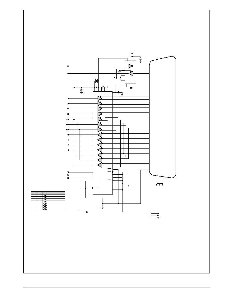
The configuration on Figure 5 uses the SP507 in a
popular DTE/DCE configuration. The TxC signal is
half-duplex and bidirectional. The DCE_ST driver is
active during DCE mode while the DTE_ST receiver
is active during DTE mode. The STEN and SCTEN
enable lines are connected together for common
DCE/DTE control. Similarly with the RL/DCD pair
and the LL/TM pair. The DCD signal is used for this
driver labelled RL in this case. The Remote Loopback
function is not available in this configuration.
The same goes for the Test Mode function where the
TM receiver is used for Local Loopback when in
DCE mode.
On-Board Programmable
DTE/DCE Configuration
(Without Crossover Cables)
DTE/DCE programmability can also be achieved
without using crossover cables. Instead, the selection
can be designed in the circuitry. This requires a
bidirectional serial port for all signals, not just TxC
and DCD. An "on-board" solution would need to
have circuitry allocated for DTE and circuitry
allocated for DCE. The transceiver portion would
need to address disable functions, low leakage
currents, and specific timing issues when joined
together in a half-duplex configuration.

5
SP505/6/7APN/03
SP505, SP506, SP507 Application Note
© Copyright 2000 Sipex Corporation
Figure 3. SP506 DCE Configuration
10
µ
F
10
µ
F
10
µ
F
27 26
30
28
31
32
1N5819, MBRS140T3, or equiv.
V
CC
V
DD
C1-
C2-
V
SS
C1+
C2+
10
µ
F
61
59
SP506CF
Drivers
TxD
14
58
56
DTR
13
54
52
RTS
16
63
65
TxC
15
42
44
ST
22
47
45
RL
17
51
49
LL
24
70
71
RxD
1
37
38
RxC
20
66
67
CTS
80
68
69
DSR
78
35
36
DCD
19
39
40
RI
21
76
77
SCT
79
Receivers
10
µ
F
DB-25 Connector Pins & Signals
3
RXD(a)
16
RXD(b)
6
DSR(a)
22
DSR(b)
13
CTS(b)
5
CTS(a)
9
RXC(b)
25
TM
n/a
n/a
DEC0
DEC1
DEC2
DEC3
9
10
11
12
SCTEN
TREN
SDEN
Various VCC pins
(Refer to SP506
Datasheet)
17
RXC(a)
2
TXD(a)
14
TXD(b)
21
RL
10 DCD(b)
Various GND pins (Refer to SP506 Datasheet)
7
SIGNAL GND (#102)
19
RTS(b)
20
DTR(a)
23
DTR(b)
11
TXCE(b)
4
RTS(a)
24
TXCE(a)
15 TXC(a)
12
TXC(b)
RSEN
RLEN
LLEN
STEN
TTEN
2
3
4
18
5
23
12
7
LATCH
8
GND
+5V
#104
#107
#106
#115
#142
#103
#113
#105
#108
#140
#141
#114
8
DCD(a)
18
LL
#109
M1 (V.28_Enable)
Mode_Enable
M2 (V.11_Enable)
M0
M3
Mode Selection
M3 M2
M1
M0
Physical Layer
0 0
0
0
SHUTDOWN
0 1
0
0
X.21 (V.11)
0 0
1
0
RS-232 (V.28)
1 1
0
0
RS-449 (V.11 & V.10)
1
1
0
1
EIA-530 (V.11 & V.10)
1
1
1
0
V.35 (V.35 & V.28)
1
1
1
1
EIA-530A (V.11 & V.10)
Mode
Enable

6
SP505/6/7APN/03
SP505, SP506, SP507 Application Note
© Copyright 2000 Sipex Corporation
Figure 4. SP506 DTE/DCE Programmable Configuration
10
µ
F
10
µ
F
10
µ
F
27 26
30
28
31
32
1N5819, MBRS140T3, or equiv.
V
CC
V
DD
C1-
C2-
V
SS
C1+
C2+
10
µ
F
61
59
SP506CF
Drivers
TxD
14
58
56
DTR
13
54
52
RTS
16
63
65
TxC
15
42
44
ST
22
47
45
RL
17
51
49
LL
24
70
71
RxD
1
37
38
RxC
20
66
67
CTS
80
68
69
DSR
78
35
36
DCD
19
39
40
RI
21
76
77
SCT
79
Receivers
10
µ
F
DB-25 Connector Pins & Signals [DTE/DCE]
2
TXD(a)/RXD(a)
14 TXD(a)/RXD(b)
20 DTR(a)/DSR(a)
23
DTR(b)/DSR(b)
19
RTS(b)/CTS(b)
4
RTS(a)/CTS(b)
11 TXCE(b)/TXC(b)
18
LL/TM
15
*TXC(a)/RXC(a)
12
*TXC(b)/RXC(b)
DEC0
DEC1
DEC2
DEC3
9
10
11
12
SCTEN
TREN
SDEN
Various VCC pins
(Refer to SP506
Datasheet)
24
TXCE(a)/TXC(a)
3
RXD(a)/TXD(a)
16
RXD(b)/TXD(b)
8
DCD(a)/RL or DCD(a)**
10
DCD(b)/DCD(b)
Various GND pins (Refer to SP506 Datasheet)
7
SIGNAL GND (#102)
13
CTS(b)/RTS(b)
6
DSR(a)/DTR(a)
22
DSR(b)/DTR(b)
9
RXC(b)/TXCE(b)
5
CTS(a)/RTS(a)
17
RXC(a)/TXCE(a)
RSEN
RLEN
LLEN
STEN
TTEN
2
3
4
18
5
23
12
7
LATCH
8
GND
* - Driver applies for DCE only on pins 24 and 11. Receiver applies for DTE
only on pins 24 and 11.
** - RL may not be required in some applications and DCD may be required
to be bi-directional. If RL is not required The RL is replaced by DCD(a)
and the #140_DCE is replaced by #109_DCE. The RL driver of the
SP505 will not be in use during DCE mode in this case.
+5V
#103_DTE/#104_DCE
#108_DTE/#107_DCE
#105_DTE/#106_DCE
#114_DTE/#114_DCE
#141_DTE/#142_DCE
#104_DTE/#103_DCE
#115_DTE/#113_DCE
#106_DTE/#105_DCE
#107_DTE/#108_DCE
#109_DTE/#140_DCE**
#142_DTE/#141_DCE
I/O Lines represented by double arrowhead signifies a bi-directional bus.
Input Line
Output Line
#113_DTE/#115_DCE
Optional bi-directional line; if RL (#140) is used, the driver output, RL(a), can go directly to pin. 21, Remote Loopback, of the DB-25.
The RLEN enable pin, if RL is used, can be permanently enabled by tying it to GND.
25
TM/LL
M1 (V.28_Enable)
Mode_Enable
M2 (V.11_Enable)
M0
M3
Mode Selection
M3 M2
M1
M0
Physical Layer
0 0
0
0
SHUTDOWN
0 1
0
0
X.21 (V.11)
0 0
1
0
RS-232 (V.28)
1 1
0
0
RS-449 (V.11 & V.10)
1
1
0
1
EIA-530 (V.11 & V.10)
1
1
1
0
V.35 (V.35 & V.28)
1
1
1
1
EIA-530A (V.11 & V.10)
Mode
Enable
DCE/DTE Control
#140_DTE/#109_DCE
21
RL/DCD(a)**

7
SP505/6/7APN/03
SP505, SP506, SP507 Application Note
© Copyright 2000 Sipex Corporation
Figure 5. SP507 DTE/DCE Programmable Configuration (Similar configuration to competitor's 3-chip solution.)
10
µ
F
10
µ
F
10
µ
F
27 26
30
28
31
32
1N5819, MBRS140T3, or equiv.
V
CC
V
DD
C1-
C2-
V
SS
C1+
C2+
10
µ
F
61
59
SP507CF
Drivers
TxD
14
58
56
DTR
13
54
52
RTS
16
63
65
TxC
15
42
44
DCE_ST
22
47
45
RL
17
51
49
LL
24
70
71
RxD
1
37
38
RxC
20
66
67
CTS
80
68
69
DSR
78
35
36
DCD
19
39
40
TM
21
76
77
DTE_ST
79
Receivers
10
µ
F
M0
M1
M2
10
11
12
STEN
RREN
RTEN
Various VCC pins
(Refer to SP507
Datasheet)
Various GND pins (Refer to SP507 Datasheet)
TMEN
SCTEN
LLEN
RLEN
TTEN
2
3
7
4
5
18
6
23
+5V
LATCH
8
GND
+5V
+5V
DB-25 Connector Pins & Signals [DTE/DCE]
2
TXD(a)/RXD(a)
14 TXD(a)/RXD(b)
20 DTR(a)/DSR(a)
23
DTR(b)/DSR(b)
19
RTS(b)/CTS(b)
4
RTS(a)/CTS(b)
11 TXCE(b)/TXC(b)
18
*LL/TM
15
*TXC(a)/RXC(a)
12
*TXC(b)/RXC(b)
24
TXCE(a)/TXC(a)
3
RXD(a)/TXD(a)
16
RXD(b)/TXD(b)
13
CTS(b)/RTS(b)
6
DSR(a)/DTR(a)
22
DSR(b)/DTR(b)
9
RXC(b)/TXCE(b)
5
CTS(a)/RTS(a)
17
RXC(a)/TXCE(a)
8
*DCD(a)/DCD(a)
10
*DCD(b)/DCD(b)
7
SIGNAL GND
#103_DTE/#104_DCE
#108_DTE/#107_DCE
#105_DTE/#106_DCE
#114_DTE/#114_DCE
#141_DTE/#141_DCE
#104_DTE/#103_DCE
#115_DTE/#113_DCE
#106_DTE/#105_DCE
#107_DTE/#108_DCE
#113_DTE/#115_DCE
DCE/DTE Control
#109_DTE/#109_DCE
* - Driver applies for DCE mode only on pins 15 and 12 for signal TxC.
Receiver applies for DTE mode only on pins 15 and 12.
Driver applies for DCE mode only on pins 8 and 10 for signal DCD.
Receiver applies for DTE mode only on pins 15 and 12.
Receiver applies for DCE mode only on pin 18 for signal LL. Driver
applies for DTE mode only on pin 18.
I/O Lines represented by double arrowhead signifies a bi-directional bus.
Input Line
Output Line
M0
M1
M2
Mode Selection
M2 M1
M0
Physical Layer
0
0
0
V.11 (RS-422)
0
0
1
EIA-530A
0
1
0
EIA-530
0
1
1
X.21
1
0
0
V.35
1
0
1
RS-449 (V.36)
1
1
0
RS-232
1
1
1
SHUTDOWN
Mode
Enable
TERM_OFF
1 SHIELD GND

8
SP505/6/7APN/03
SP505, SP506, SP507 Application Note
© Copyright 2000 Sipex Corporation
Figure 6. Complete DTE/DCE Programmable Serial Port w/o Crossover Cables
Connector Pins DTE/DCE
[DB-25 EIA-530, ISO-2593 V
.35]
Symbol
2, P
TXD(a)/RXD(a)
14, S
TXD(b)/RXD(b)
20, H
DTR(a)/DSR(a)
4, C
R
TS(a)/CTS(a)
1
1, W
TXCE(b)/RXC(b)
18, L
LL/TM
24, U
TXCE(a)/RXC(a)
3, R
RXD(a)/TXD(a)
16, T
RXD(b)/TXD(b)
22
DSR(b)/DTR(b)
6, E
DSR(a)/DTR(a)
9, X
RXC(b)/TXCE(b)
5, D
CTS(a)/R
TS(a)
17, V
RXC(a)TXCE(a)
25, NN
TM/LL
21, N
RL(a)/RL(a)
10
µ
F1
0
µ
F
10
µ
F
27
26
30
28
31
32
1N5819, MBRS140T3, or equiv
.
V
CC
V
DD
C1-
C2-
V
SS
C1+
C2+
10
µ
F
61
59
SP506
Drivers
TxD
14
58
56
DTR
13
54
52
RT
S
16
63
65
TxC
15
42
44
ST
22
47
45
RL
17
51
49
LL
24
70
71
RxD
1
37
38
RxC
20
66
67
CTS
80
68
69
DSR
78
35
36
DCD
19
39
40
RI
21
76
77
SCT
79
Receivers
10
µ
F
DEC3
DEC2
DEC1
DEC0
12
11
10
9
SCTEN
TREN
SDEN
V
arious VCC pins (Refer
to SP506 Datasheet)
#103/#104
#108/#107
#105/#106
to HDLC
#141/#142
#104/#103
#1
15/#1
13
#106/#105
#107/#108
#109
#142/#141
V
arious GND pins (Refer to SP506 Datasheet)
RSEN
RLEN
LLEN
STEN
TTEN
2
3
4
18
5
23
12
7
+5V
LA
TCH
8
GND
+5V
#140
5
4
1
2
3
6
7
8
5
4
1
2
3
6
7
8
8
7
1
2
3
4
5
6
Semtech
LCDA15C-6
Semtech
LCDA15C-6
10
µ
F1
0
µ
F
10
µ
F
27
26
30
28
31
32
1N5819, MBRS140T3, or equiv
.
V
CC
V
DD
C1-
C2-
V
SS
C1+
C2+
10
µ
F
61
59
SP506
Drivers
TxD
14
58
56
DTR
13
54
52
RT
S
16
63
65
TxC
15
42
44
ST
22
47
45
RL
17
51
49
LL
24
70
71
RxD
1
37
38
RxC
20
66
67
CTS
80
68
69
DSR
78
35
36
DCD
19
39
40
RI
21
76
77
SCT
79
Receivers
10
µ
F
DEC3
DEC2
DEC1
DEC0
12
11
10
9
SCTEN
TREN
SDEN
V
arious VCC pins (Refer
to SP506 Datasheet)
V
arious GND pins (Refer to SP506 Datasheet)
RSEN
RLEN
LLEN
STEN
TTEN
2
3
4
18
5
23
12
7
+5V
LA
TCH
8
GND
+5V
23
DTR(b)/DSR(b)
19
R
TS(b)/CTS(b)
13
CTS(b)/R
TS(b)
8, F
DCD(a)/DCD(a)
10
DCD(b)/DCD(b)
12, AA
TXC(b)/TXC(b)
15, Y
TXC(a)/TXC(a)
+5V
+5V
8
7
1
2
3
4
5
6
Semtech
SMDA15C-7
Semtech
SMDA15C-7
DTE/DCE
#1
13/#1
15
#1
14
T
ranszorbs are optional for added protection against ESD and over
-voltage
transients. Recommended are Semtech'
s LCDA15C-6 on the clock and data
lines (low capacitance for high speed signals) and SMDA15C-7 on the
control/handshaking lines.
N/C
N/C
N/C
N/C
N/C
N/C
N/C
N/C
N/C
N/C
N/C
N/C
SP506 for DTE
SP506 for DCE
Mode
D_E
M7
M6
M5
M4
M3
M2
M1
M0
RS-232
DTE
0
0
1
0
0
0
0
0
EIA-530
DTE
1
1
0
1
0
0
0
0
RS-449
DTE
1
1
0
0
0
0
0
0
V
.35
DTE
1
1
1
0
0
0
0
0
X.21
DTE
0
1
0
0
0
0
0
0
V
.36
DTE 0
1
1
0
0
0
0
0
RS-232
DCE
0
0
0
0
0
0
1
0
EIA-530
DCE
0
0
0
0
1
1
0
1
RS-449
DCE
0
0
0
0
1
1
0
0
V
.35
DCE
0
0
0
0
1
1
1
0
X.21
DCE
0
0
0
0
0
1
0
0
V
.36
DCE 0
0
0
0
0
1
1
0
Control Logic from FPGA
or PLD
M7
M6
M5
M4
M3
M2
M1
M0
N/C
N/C
N/C
Semtech
SL
VG2.8
T
ranszorbs can be added to the digital
I/Os for daughter board configurations
where the interface card may be hot
inserted into another board. Semtech'
s
SL
VG2.8 or similar will protect against
ESD or over
-voltage transients during
hot insertion.
The rated clamping range
is from -0.6V
to +5.3V
.
SL
VG2.8
SL
VG2.8
SL
VG2.8
SL
VG2.8
SL
VG2.8
SL
VG2.8
SL
VG2.8
SL
VG2.8
SL
VG2.8
SL
VG2.8
SL
VG2.8
SL
VG2.8
SL
VG2.8
SLV
G2.8
SLV
G2.8
SLV
G2.8
SLV
G2.8
SL
VG2.8
SL
VG2.8
SL
VG2.8
SL
VG2.8

9
SP505/6/7APN/03
SP505, SP506, SP507 Application Note
© Copyright 2000 Sipex Corporation
The SP505, SP506 and SP507 can be easily designed
to support this type of configuration. Figure 6 shows
a typical circuit illustrating two SP506 devices
connected in a half-duplex configuration. The top
circuit is dedicated to DTE and the bottom SP506 is
dedicated to DCE. Note that only one device is active
at any given time. For DTE, the decoder for the DCE
device should be off (0000), and vice versa. During
the shutdown or off state of the SP506, the driver
output typically draws 100
µ
A of leakage current.
Even with the maximum SP506 leakage current of
500
µ
A, the receiver input impedance would only
change by 500
. This is important for RS-232 since
the input voltage range can be up to 15V and the
typical RS-232 receiver input impedance is 5k
.
For V.11 differential receivers, the maximum range
is +7V and typical input impedance is 10k
. Thus for
V.28 receivers, the drivers would be effectively
driving into 5k
in parallel with the disabled
receiver with 10k
input impedance. The resultant
impedance is 3.3k
. For V.11 mode, the drivers will
drive into either a terminated receiver of 120
or
unterminated receiver at 3.9k
.
These two values in
parallel with the disabled 10k
receiver will yield
118
and 2.8k
, respectively, and will not degrade
the V.11 driver performance. The receiver outputs are
typically at 1
µ
A when disabled.
The SP505, SP506 and SP507 adds convenience
by incorporating the V.11 and V.35 termination
resistors inside the device. For this type of 2-chip
DTE/DCE configuration, the termination resistors
would need to be disabled along with the receivers.
A "0000" code into the SP505 and SP506 will
automatically disable all termination networks as
well as the transceivers. A "111" code into the SP507
performs the same function. In the shutdown mode,
the IC will draw less than 10mA of supply current.
Adding Additional Transceivers
To support additional signals, the SP522 can easily
attach onto the SP505, SP506 or SP507 charge pump
outputs, V
DD
and V
SS
. The SP522 adds two drivers
and two receivers for supporting other signals such
as RI and RL. In Figure 7, the SP522 is hardwired for
RS-423 or ITU-T V.10 mode. This allows for the
support of RI and RL in RS-449 or V.35 modes if
necessary.
Schottky Diode on the SP50x
Sipex requires the installation of a Schottky rectifier
placed between the V
CC
and V
DD
pins of the SP50x
charge pump, where the anode is connected to V
CC
and the cathode is connected to V
DD
. It is required to
bootstrap the charge pump's internal circuitry during
power off conditions in presence of signals or voltages
through the receiver inputs or driver outputs.
When placed in parallel with the charge pump
capacitor, the diode will allow some of the V
CC
current to flow into the V
DD
regions of the device,
which will partially bias the V
DD
charged regions
before the device charge pump is fully functioning.
This prevents biasing of V
DD
from other sources
such as through the driver outputs or receiver inputs,
typical of serial port connections to other powered-on
equipment. Once the charge pump oscillator starts up
and becomes functional, current flows from V
DD
back
into V
CC
through the capacitor, ensuring that a
rapidly rising V
DD
does not rise too quickly above the
V
CC
regions before the V
CC
regions have become
fully charged.
The main characteristics of the Schottky diode
necessary for this application is the forward
voltage. The V
F
of the 1N5819 type, which is the
diode recommended, is 0.6V @ 1A. Surface mount
versions are available from Motorola. The
MBRS130T3 from Motorola is used with our SP505,
SP506, and SP507 evaluation boards. Other options
are MBRS140T3 or MBRS130LT3, which are all in a
"403A-03 SMB" package. The end-to-end length is
5.40mm typical and the width is 3.55mm typical.
Motorola also offers the Powermite
TM
line, which
offers the Schottky rectifiers in a 1.1mm height,
3.75mm length, and 1.90mm width surface mount
package. The part numbers recommended are
MBRM120LT3, MBRM120ET3, and MBRM140T3.
Specifics can be found in Motorola Semiconductor's
web site (http://mot-sps.com/products/index.html).
The Schottky rectifiers can be found in the discrete
rectifier section and datasheets can be downloaded
after searching for the part number.
Powermite
TM
is a trademark of Motorola.
10
SP505/6/7APN/03
SP505, SP506, SP507 Application Note
© Copyright 2000 Sipex Corporation
Figure 7. Adding the SP522 to the SP507 in a DTE/DCE Programmable Configuration
22
µ
F
22
µ
F
22
µ
F
27 26
30
28
31
32
1N5819, MBRS140T3, or equiv.
V
CC
V
DD
C1-
C2-
V
SS
C1+
C2+
22
µ
F
61
59
SP507CF
Drivers
TxD
14
58
56
DTR
13
54
52
RTS
16
63
65
TxC
15
42
44
DCE_ST
22
47
45
RL
17
51
49
LL
24
70
71
RxD
1
37
38
RxC
20
66
67
CTS
80
68
69
DSR
78
35
36
DCD
19
39
40
TM
21
76
77
DTE_ST
79
Receivers
10
µ
F
M0
M1
M2
10
11
12
STEN
RREN
RTEN
Various VCC pins
(Refer to SP507
Datasheet)
Various GND pins (Refer to SP507 Datasheet)
TMEN
SCTEN
LLEN
RLEN
TTEN
2
3
7
4
5
18
6
23
+5V
LATCH
8
GND
+5V
+5V
DB-25 Connector Pins & Signals [DTE/DCE]
2
TXD(a)/RXD(a)
14 TXD(a)/RXD(b)
20 DTR(a)/DSR(a)
23
DTR(b)/DSR(b)
19
RTS(b)/CTS(b)
4
RTS(a)/CTS(b)
11 TXCE(b)/TXC(b)
21
*RL/RL
15
*TXC(a)/RXC(a)
12
*TXC(b)/RXC(b)
24
TXCE(a)/TXC(a)
3
RXD(a)/TXD(a)
16
RXD(b)/TXD(b)
13
CTS(b)/RTS(b)
6
DSR(a)/DTR(a)
22
DSR(b)/DTR(b)
9
RXC(b)/TXCE(b)
5
CTS(a)/RTS(a)
17
RXC(a)/TXCE(a)
8
*DCD(a)/DCD(a)
10
*DCD(b)/DCD(b)
7
SIGNAL GND
#103_DTE/#104_DCE
#108_DTE/#107_DCE
#105_DTE/#106_DCE
#114_DTE/#114_DCE
#140_DTE/#140_DCE
#104_DTE/#103_DCE
#115_DTE/#113_DCE
#106_DTE/#105_DCE
#107_DTE/#108_DCE
#113_DTE/#115_DCE
DCE/DTE Control
#109_DTE/#109_DCE
* - Driver applies for DCE mode only on pins 15 and 12 for signal TxC.
Receiver applies for DTE mode only on pins 15 and 12.
Driver applies for DCE mode only on pins 8 and 10 for signal DCD.
Receiver applies for DTE mode only on pins 15 and 12.
Receiver applies for DCE mode only on pin 18 for signal LL. Driver
applies for DTE mode only on pin 18.
I/O Lines represented by double arrowhead signifies a bi-directional bus.
Input Line
Output Line
M0
M1
M2
Mode Selection
M2 M1
M0
Physical Layer
0
0
0
V.11 (RS-422)
0
0
1
EIA-530A
0
1
0
EIA-530
0
1
1
X.21
1
0
0
V.35
1
0
1
RS-449 (V.36)
1
1
0
RS-232
1
1
1
SHUTDOWN
Mode
Enable
TERM_OFF
1 SHIELD GND
10
µ
F
+5V
V
SS
V
DD
V
CC
GND
#141_DTE/#125_DCE
#125_DTE/#141_DCE
DP0
DP1
+5V
18
LL/TM
25
TM/LL
LBK
T1OUT
R1IN
T1IN
R1OUT
ENT1
ENR1
SP522

11
SP505/6/7APN/03
SP505, SP506, SP507 Application Note
© Copyright 2000 Sipex Corporation
SP506 and SP507 Drive Capability
According to the ITU-T V.11 standard, the maximum
cable length for a differential V.11 transmission is
4,000 feet (~1,000 meters). However, the standard
also illustrates a derating graph of data rate versus
cable length. So actually in a real application, the
system would not be able to transmit 10Mbps over
the full 4,000 feet of Category 3 or similar type cable.
As cable parasitics add up over longer cable lengths,
capacitance and other affects will degrade the signal,
especially at higher frequencies.
The signal integrity depends mainly on the driver
output strength or "drivability" and parasitic
capacitance on the cable. RS-232 cabling is typically
50pF per foot, where as a good twisted pair type
cable for X.21, RS-449, EIA-530, or V.35 will
typically be 10pF per foot or less. Some better quality
cables will have 3-5pF per foot.
Using a typical setup with a TTC Fireberd 6000A Bit
Error Rate Tester (BERT) connected with our SP507
evaluation board as configured in Figure 8 below,
the driver output performance was characterized
over various cable lengths. The 6000A BERT
emulated the DCE, which provided the TXC clock
pulse from 1.544Mbps to 12Mbps. The clock waveform
was propagated through the serial cable to the SP507
evaluation board, which was configured as the DTE.
The clock signal was then "echoed" through the
TxCE (Transmit Clock Echo) driver across the cable
and back the BERT. The clock signal input to the
TxCE driver (CH3) and the differential driver output
are measured with a oscilloscope to observe driver
waveform integrity. The differential driver output
was measured at the other end of the cable (M1 =
A - B), as if the receiver would view the incoming
signal. The data stream was generated by the DCE
and was propagated through the SP507's RxC
receiver and TxCE driver. The BERT also records
the number of bit errors occurring during the infinite
1:1 data bit stream that is sent back through the cable.
Figure 8. SP507 Cable Length Versus Throughput Circuit Configuration
22
µ
F
22
µ
F
22
µ
F
27 26
30
28
31
32
MBRS140T3
V
CC
V
DD
C1-
C2-
V
SS
C1+
C2+
22
µ
F
61
59
SP507CF
TxD
14
58
56
DTR
13
54
52
RTS
16
63
65
TxCE
15
42
44
ST
22
47
45
RL
17
51
49
LL
24
70
71
RxD
1
37
38
RxC
20
66
67
CTS
80
68
69
DSR
78
35
36
DCD
19
39
40
TM
21
76
77
SCT
79
10
µ
F
M0
M1
M2
10
11
12
STEN
RREN
RTEN
Various GND pins (Refer to SP507 Datasheet)
TMEN
SCTEN
LLEN
RLEN
TTEN
2
3
7
4
5
18
6
23
+5V
LATCH
8
GND
+5V
+5V
Fireberd 6000A
Network/BER Tester
TxD
RxD
DTR
DSR
CTS
DCE (emulated)
DTE (Evaluation Board)
CH3
M1
RTS
RxC
DCD
TxC
TxC
Notes: V.35 Mode selected.
Open Driver Inputs
are default as HIGH.
"1"
"0"
"0"
Signal GND
Cab
le Length used:
6ft.
to 156ft.

12
SP505/6/7APN/03
SP505, SP506, SP507 Application Note
© Copyright 2000 Sipex Corporation
Figure 12. SP507 TxCE at 2.048MHz over 156ft.
Figure 13. SP507 TxCE at 6.312MHz over 6ft.
Figure 14. SP507 TxCE at 6.312MHz over 56ft.
Figure 10. SP507 TxCE at 2.048MHz over 56ft.
Figure 11. SP507 TxCE at 2.048MHz over 106ft.
Figure 9. SP507 TxCE at 2.048MHz over 6ft.

13
SP505/6/7APN/03
SP505, SP506, SP507 Application Note
© Copyright 2000 Sipex Corporation
Figure 15. SP507 TxCE at 6.312MHz over 106ft.
Figure 16. SP507 TxCE at 6.312MHz over 156ft.
Figure 17. SP507 TxCE at 8.192MHz over 6ft.
Figure 19. SP507 TxCE at 8.192MHz over 106ft.
Figure 18. SP507 TxCE at 8.192MHz over 56ft.
Figure 20. SP507 TxCE at 8.192MHz over 156ft.

14
SP505/6/7APN/03
SP505, SP506, SP507 Application Note
© Copyright 2000 Sipex Corporation
Figure 25. SP507 TxCE at 12MHz over 6ft.
Figure 24. SP507 TxCE at 10MHz over 156ft.
Figure 26. SP507 TxCE at 12MHz over 56ft.
Figure 21. SP507 TxCE at 10MHz over 6ft.
Figure 22. SP507 TxCE at 10MHz over 56ft.
Figure 23. SP507 TxCE at 10MHz over 106ft.
15
SP505/6/7APN/03
SP505, SP506, SP507 Application Note
© Copyright 2000 Sipex Corporation
Figure 27. SP507 TxCE at 12MHz over 86ft.
The V.35 interface was selected because the V.35
signal has low voltage differential amplitude, which
is more susceptible to noise compared to other higher
amplitude signals such as V.11 or RS-485. The small
amplitude of 0.55V can easily be affected by noise
caused by various environmental effects.
SP506 and SP507 driver performance was
characterized over 6ft., 26ft., 56ft., 86ft, 106ft., 126ft.,
and 156ft. V.35 cable lengths. The frequency
measured are from 1.544MHz, 2.048MHz,
3.152MHz, 6.312MHz, 8.192MHz, 9.600MHz,
10MHz, and 12MHz. The scope photos and graphs
on Figures 9 through 27 illustrate the some of these
measurements.
The Fireberd 6000A was able to synchronize with
the incoming TxCE clock signal and read the TxD
output data stream up to a 12MHz clock without any
bit errors. This implies that the clock source had
sufficient amplitude and was stable enough for the
DCE receiver to read back and synchronize the data
on the clock's rising edge. The transmission was
successful up to 12MHz with 86 feet of V.35 cable
without bit errors. Further cable length degraded the
signal to a point where the receiver was unable to
capture the clock, thus not able to synchronize data
and resulting in bit errors.
One important note is that the signal no longer
adheres to the V.35 specification for Transmitter
Differential Output with Termination (per CCITT
V.35 Section II.3.c) of 0.44V minimum after 56 feet
at 10MHz. However, longer cable lengths and even
12MHz signaling was still readable by the DCE. This
is because the V.35 receiver input sensitivity is
200mV maximum. As the signal amplitude decays to
approximately 400mV
P
(832mV
P-P
), there is still
enough gain on the signal for the receiver to
successfully read the clock. Although the AC
performance across the system is worse as the
receiver input sensitivity is higher.
The V.35 specification does not take into account any
capacitive loading for the Terminated Transmitter
Output measurement. Therefore it would be unfair to
use the V.35 specification as a criteria for pass/fail in
a real application environment. Signal monotonicity
and duty cycle are the important, measurable
elements to determining a clean and error-free
clock transmission.
Note that these oscilloscope photos are a typical
representation of the SP507's performance in
presence of cabling using our in-house evaluation
board. The system designer should test and
characterize the system in order determine the cable
distance versus speed allowance in the application.
16
SP505/6/7APN/03
SP505, SP506, SP507 Application Note
© Copyright 2000 Sipex Corporation
ESD Protection and EMI Filtering
It is now a requirement for networking equipment,
in order to receive the European "CE" mark, to
withstand a certain amount of environmental
hazards. Among these are ESD and EMI immunity as
well as EMI emissions, which is the equipment's
own generation of electromagnetic interference.
Electrostatic discharge and overvoltage transients
are important to suppress in any system. The
specification generally used for ESD immunity is
EN61000-4-2 (formerly IEC1000-4-2), which
specifies Air Discharge and Contact Discharge
Methods. For "CE" approval, the acceptance level
is generally "Level 2" per the IEC1000-4-2
specification, which is 4kV Air Discharge and 4kV
Contact Discharge. While the SP505, SP506, and
SP507 has reasonable handling withstand voltages
built in the I/O structures of the device, external
protection is always a good idea.
One method of protection is incorporating
TransZorbs
TM
or transient voltage suppression ICs,
which are back-to-back Zener diodes connected on
the line to ground. There are a variety of manufacturers
such as Motorola, Siemens, Semtech, Protek Devices,
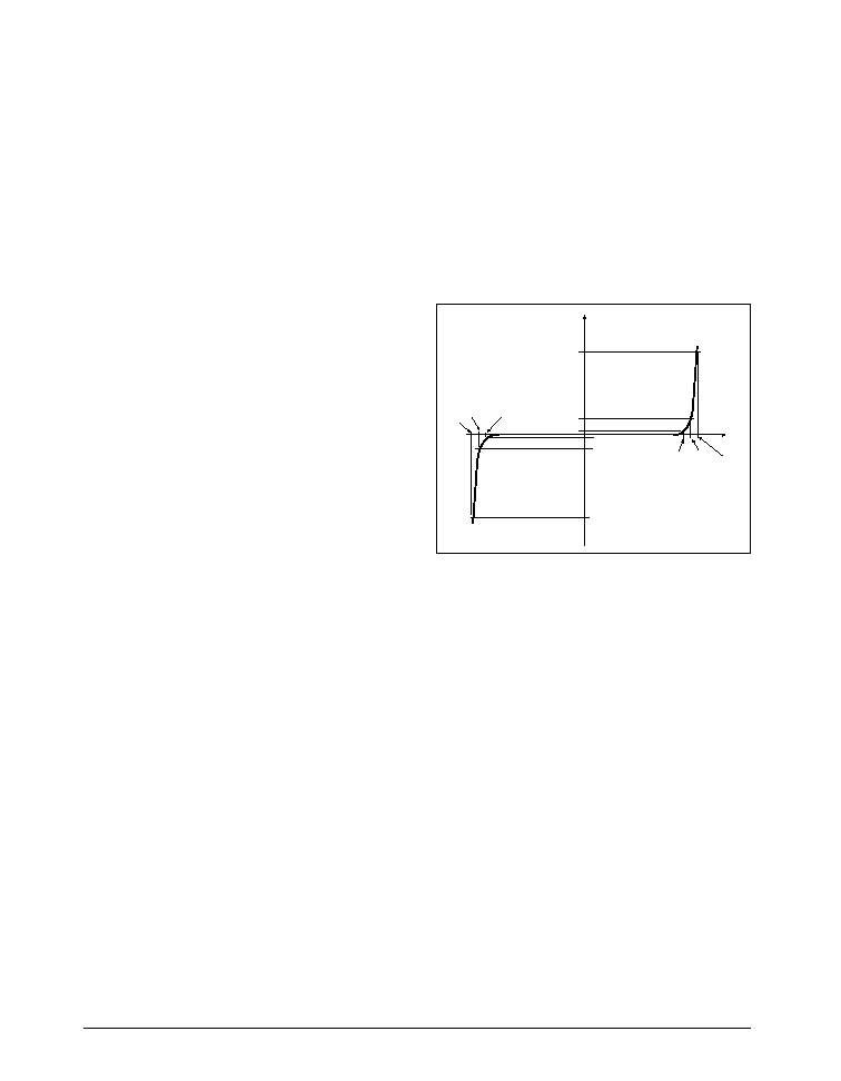
and more. The key specifications are:
1)
Reverse Standoff Voltage - normal circuit operating
voltage. For RS-232, the maximum V
RWM
= 15V.
2)
Peak Pulse or Transient Current - expected transient
current. (I
PP
)
3)
Reverse Breakdown Voltage - device begins to
avalanche and becomes a low impedance path to
ground for the transient. (V
BR
)
4)
Maximum Junction Capacitance - loading capacitance
of the diode structure. More capacitance will affect the
total AC performance. (C
J
)
A variety of transzorbs were tested and all perform
well in the presence of ESD transients. For faster data
rates such as V.11 and V.35 signals, low capacitance
is important since an additional 50pF load could add
5ns to the transition time and affect the overall
transmission rate. The Semtech LCDA15C-6 and
Protek Devices SM16LC15C are especially designed
for data communications because of the multichannel
line support and the low junction capacitance.
Figure 29 illustrates a TVS configuration using the
Semtech LCDA15C-6 connected to the clock and
data signals of the SP505, SP506 and SP507.
The LCDAC-6 was chosen due to its low junction
capacitance of 20pF, which are important for high
speed clock and data lines. Protek's SM16LC15C can
also be used as the junction capacitance is 25pF.
However, the two TVS devices are not pin compatible.
Protek's SM16LC15C contains protection for eight
lines and has a straight-through pinout. One side of
the SM16LC15C is grounded. The LCDAC-6 uses a
8-pin SOIC package as opposed to the 16-pin
package with the SM16LC15C. Since two ICs are
needed anyway for clock and data, the smaller
package is usually preferred. Refer to each of the
manufacturer's datasheet for details. Figure 30
illustrates a TVS configuration to the handshaking
signals. As these signals are for control and indication,
they do not usually switch at high speed. The junction
capacitance for these devices are less critical.
Figure 28. I-V Curve of a TVS diode
Lower V
RWM
values can be selected instead of 15V.
If the configuration is straightforward, using 5V to
8V V
RWM
values is fine for the driver outputs and
receiver inputs. Using 5V V
RWM
on the driver is fine
since the clamping occurs at the reverse breakdown
voltage(V
BR
), which is 6V for most 5V transzorbs.
However, during compliancy testing, the V.28
receiver may be subjected to 15V in order to test the
input impedance. Applying a voltage exceeding the
V
RWM
rating will affect the input current measurement
and thus fail the impedance test.
TransZorb
is a trademark of General Semiconductor Industries.
V
rwm
V
rwm
I
r
I
r
V
br
V
br
I
t
I
t
V
c
V
c
I
pp
I
pp
I
V

17
SP505/6/7APN/03
SP505, SP506, SP507 Application Note
© Copyright 2000 Sipex Corporation
Figure 29. TVS Configuration to Clock and Data Lines of the SP505/SP506/SP507
Figure 30. TVS Configuration to Handshaking Signal Lines of the SP505/SP506/SP507
5
4
1
2
3
6
7
8
Semtech
LCDA15C-6
TxD(a)
TxD(b)
TxCE(a)
TxCE(b)
TxCE(a)
TxCE(b)
RxD(a)
RxD(b)
RxC(a)
RxC(b)
5
4
1
2
3
6
7
8
Semtech
LCDA15C-6
Signal
GND
RTS(a)
RTS(b)
DTR(a)
DTR(b)
DCD(a)
DCD(b)
CTS(a)
CTS(b)
DSR(a)
DSR(b)
Signal
GND
8
7
1
2
3
4
5
6
8
1
2
3
4
5
Semtech
SMDA15C-7
Semtech
SMDA15C-5
LL
TM

18
SP505/6/7APN/03
SP505, SP506, SP507 Application Note
© Copyright 2000 Sipex Corporation
the power supply unit and radiated out to the
environment. For serial port datacom applications,
both emissions and immunity must be carefully
considered during the design-in phase.
The conducted emissions in the most single supply
interface transceivers are generated from the internal
charge pump. Although the charge pump is enhanced
over previous generation pumps, the SP506 and
SP507 charge pump architecture will inherently have
small ripples on the V
DD
and V
SS
outputs. The ripples
are due to the switching of the internal charge pump
transistors that are transferring energy. The charge
pump oscillates at 20kHz in standby mode (without
loads to the drivers) and will automatically increase
frequency to 300kHz when loaded. The ripples will
coincide with the oscillator frequency. The driver
output circuitry receives biasing from the charge
pump outputs, V
DD
and V
SS
, for the V.28 and V.10
bipolar voltage swings. The V
DD
or V
SS
supply ripple
could be superimposed onto the driver outputs,
depending on the ripple amplitude. Larger capacitor
values will suppress the ripple of the pump and thus,
minimize the ripple amplitude on the data lines.
For the SP505, SP506, and SP507, the amplitude of
the ripple is below 100mV when using 22
µ
F pump
capacitors (refer to Figure 34).
Depending on the application requirements, EMI/EMC
filtering may be needed. The SP506
and SP507 are
usually not affected by radiated disturbance nor do
they emit radiated noise/interference. But a shielded
enclosure (Faraday Cage) will help the immunity from
radiated disturbance as well as emissions of radiated
noise. Conducted noise can be surpressed by using
ferrite beads, low pass filters using RC circuits,
inductor circuits, or common mode chokes on the
signal lines.
One surface mount common-mode choke (CMC)
designed for data signaling applications in the 10Mbps
to 15Mbps band is TDK's ZJYS51R5-4P. This 8-pin
SOIC package contains a two pairs of inductors for
two differential signals. Since clock and data are
switching most frequently, the number of pairs needed
are two for DTE (TxD and TxCE drivers) or three for
DCE (TxD, TxCE, TxC drivers), which means one
IC for DTE and two ICs for DCE. Refer to Figure 31
for connection and to TDK's datasheet for the
ZJYS51R5-4P CMC.
(http://www.tdk.co.jp/tefe02/e971_zjys.pdf)
Semtech's SMDA15C-7 is used in Figure 30 to protect
the handshaking signals. Since the SMDA15C-7 only
provides protection for seven lines, the SMDA15C-5
is used for the remaining lines. Both are 8-pin SOIC
packages. Other configurations or manufacturers
can be used. Refer to the TVS datasheets.
(http://www.semtech.com/pdf/tvs/lcda15c6.pdf)
Figure 6 also shows optional TransZorbs
TM
or TVS
devices on the SP506 to further protect the serial
port from any ESD or overvoltage transients that
may occur in any application. The SP505, SP506
and SP507 are internally rated for 8kV based on
Human Body Model and 2kV Air Discharge per
IEC1000-4-2. Adding transzorbs to the I/O lines will
protect the serial port to over 15kV of ESD transients
per IEC1000-4-2 Air Discharge and 8kV per Contact
Discharge. The TVS devices on the driver inputs
and receiver outputs are included for hot-insertion
of the interface module/board applications.
The internal junction of the SP505, SP506 and SP507
receiver inputs and driver outputs are similar to the
I-V curve on Figure 28. However, TVS devices are
always recommended where ever possible as it is
difficult to predict transient induced phenomena in
any environment.
It is also important to know that these TVS devices
are also specified for IEC1000-4-4 Electrical Fast
Transients and IEC1000-4-5 Surge (Lightning)
protection. Refer to the TVS datasheets from Semtech
for details (www.semtech.com).
Electromagnetic Interference is also a concern for
networking equipment. The EMI noise is cause by
radiated emissions or power-line conducted emissions
from the system. The equipment has to be characterized
for both immunity and emissions. Immunity is the
system's tolerance to incoming interference or
disturbances generated from outside sources.
Emissions are the system's own generation of these
types of disturbances. Specifically, the documents
EN61000-4-3 and EN61000-4-6 pertain to Radiated
electric field test and Line Conducted electric field
test, respectively, for immunity. The EN55022
specification pertains to emissions and specifies
Line Conducted Emission, which are noise or
disturbances generated from a power supply unit,
conducted in the cables; and Radiated emissions,
which pertain to noise or disturbances generated by

19
SP505/6/7APN/03
SP505, SP506, SP507 Application Note
© Copyright 2000 Sipex Corporation
Another alternative is using conductive-EMI
enhanced connectors that have ferrite cores around
the pins. AMP and other connector manufacturers
also offer specially built conductive-EMI filtered
connectors. The AMPLIMITE
TM
Subminiature D-Sub
connectors have a DB-15 through DB-37 connectors
as well as high density connectors that have a
distributed element filter using lossy ferrite core or
a capacitive filter assembled around each pin. These
connectors have right-angle, vertical, or stacked
versions that all have the same PCB footprint as the
regular non-filtered connectors.
Various filter types are available with these connectors.
Once the serial protocol is defined and the operating
frequency known, a filter type can be chosen using
its 3dB point, which can be used as the maximum
frequency. The filter will begin filtering above this
3dB point. One should be careful when using the
capacitive filters as they will affect the overall AC
performance of the driver, specifically driver rise/
fall time. Details of the AMPLIMITE
TM
filtered
connectors can be found in AMP's home page
(http://connect.amp.com.), which includes insertion
loss (dB) versus frequency.
Figure 31. Common-Mode Choke Circuit with Drivers
AMPLIMITE
TM
is a trademark of AMP Inc.
1
2
3
4
5
6
7
8
L1
L2
L3
L4
TxD
TXCE

20
SP505/6/7APN/03
SP505, SP506, SP507 Application Note
© Copyright 2000 Sipex Corporation
Using Smaller Charge Pump
Capacitors with the SP50x
The charge pump of the SP505, SP506, and SP507
have been designed to drive the RS-232 voltage
levels through the drivers using 22
µ
F pump
capacitors. However, the SP505, SP506, and SP507
can use 10
µ
F capacitors for operation while still
maintaining the critical specifications.
There are two issues involved with lowering the
charge pump capacitors; RS-232 driver output V
OH
and V
OL
levels, and output ripple.
Figure 32 shows the typical driver output (TxD in
this case) in an unloaded condition using 10
µ
F charge
pump capacitors. Figure 33 shows the same driver
Figure 32. Unloaded Driver Output Using 10
µ
F Pump
Capacitors
but loaded with 3k
and 2,500pF to ground.
Running at a worse case speed of 120kHz, the driver
output voltages shown in Figure 34 clearly comply
with the RS-232 and ITU-T V.28 specifications
under these conditions.
Figures 34 and 35 show the driver output's ripple
when a DC input is asserted. The ripple in Figure 34
uses 22
µ
F charge pump capacitors where as
Figure 35 uses 10
µ
F capacitors. The ripple amplitude
is increased from approximately 60mV to 400mV.
Although the RS-232 voltages are within the
specifications and the ripple amplitude is negligible
compared to the RS-232 signal amplitude, the
designer should examine the EMC consequences of
reducing the charge pump capacitors.
Figure 33. Driver Output Loaded w/ 3k
// 2,500pF
Using 10
µ
F Pump Capacitors
Figure 34. Charge Pump Ripple of Driver Output
w/ 22
µ
F Pump Capacitors
Figure 35. Charge Pump Ripple of Driver Output
w/ 10
µ
F Pump Capacitors

21
SP505/6/7APN/03
SP505, SP506, SP507 Application Note
© Copyright 2000 Sipex Corporation
SP506 and SP507 Evaluation Boards
For easy bench testing of the SP506 and SP507,
evaluation boards are available. Similar to the
SP505EB, the SP506EB and SP507EB offers a
"breakout" type configuration that allows the user to
access the driver's and receiver's I/Os. The evaluation
boards have a DB-25 serial connector that is
configured to a EIA-530 DTE pinout. This connector
can be used to analyze any of the serial standards
offered in the SP506 and SP507. Translation cables
may be needed from the DB-25 to the appropriate
connector. Refer to Figure 1 or the cabling schemes
in the Design Guide for Multi-Protocol Serial Ports.
Refer to the SP504/SP505 Evaluation Board Manual
for the SP506EB.
For the SP507EB, the probe pins or access points are
arranged such that the drivers are on one side and the
receivers are on the other. Each driver has three basic
access points: the TTL input, inverting analog
output, and non-inverting analog output. Additional
access points are included for the driver outputs, thus
a total of four access points for each driver. Similarly
with the receiver with two analog inputs, inverting
and non-inverting, and the TTL output. Receiver
inputs have additional access points for convenience.
There are additional ground points for convenient
resistor or capacitor load connections to the driver
output access points. There are also receiver ground
points for convenience at each receiver.
The TTL control lines have DIP switches that allow
the user to input a signal to enter a logic HIGH or
logic LOW. The control lines include the driver and
receiver enable lines and the mode select pins.
For the SP506EB, the driver enable inputs are
active LOW and have internal pull down resistors.
The DIP switch position will either tie the inputs to a
logic HIGH or leave the input open where the internal
pull-down defines a LOW state.
For the SP507EB, the SP507 uses a logic HIGH for
its driver enable lines except for the LL driver, which
Figure 36. SP507EB Schematic
27 26
30
28
31
32
D1 = MBRS140T3 Schottky Rectifier
V
CC
V
DD
C1-
C2-
V
SS
C1+
C2+
61
59
SP507CF
TxD
14
58
56
13
54
52
16
63
65
15
42
44
22
47
45
17
51
49
24
70
71
1
37
38
20
66
67
80
68
69
78
35
36
19
39
40
21
76
77
79
10
µ
F
M0
M1
M2
10
11
12
STEN
RREN
RTEN
TMEN
SCTEN
LLEN
RLEN
TTEN
2
3
7
4
5
18
6
23
LATCH
GND
DB-25 Connector Pins & Signals [DTE]
2
SD(a)
14 SD(a)
20 TR(a)
23
TR(b)
19
RS(b)
4
RS(a)
11 TT(b)
18
LL(a)
15
SCT(a)
12
SCT(b)
24
TT(a)
3
RD(a)
16
RD(a)
13
CS(b)
6
DM(a)
22
DM(b)
9
RT(b)
5
CS(a)
17
RT(a)
8
RR(a)
10
RR(b)
7
SIGNAL GND
M0
M1
M2
Mode Selection
M2 M1
M0
Physical Layer
0
0
0
V.11 (RS-422)
0
0
1
EIA-530A
0
1
0
EIA-530
0
1
1
X.21
1
0
0
V.35
1
0
1
RS-449 (V.36)
1
1
0
RS-232
1
1
1
SHUTDOWN
Mode
Enable
TERM_OFF
25
TM(a)
21
RL(a)
1 SHIELD GND
DTR
RTS
TxC
DCE_ST
RL
LL
RxD
RxC
CTS
DSR
DCD
TM
DTE_ST
V
CC
25 33 41 48 55 62 73 74
V
CC
OFF
ON
V
CC
LATCH
TERM_OFF
ON
OFF
V
CC
GND located next to each
driver output & receiver input
C1 C2
C4
C3
D1
C1 ~ C4 = 22
µ
F Kemet T491C226K016AS
Decoupling Capacitor = 10
µ
F Kemet T351C106K10AS301
FUSE, jumper or
50ohm 1/4W resistor
RL(b)
LL(b)
ST(a)
ST(b)
TM(b)
SP507 Evaluation Board
Customer :
Title :
Date :
Doc. # :
Rev.
Original : June 9, 1999
A
Reference Design Schematic
233 South Hillview Dr. ∑ Milpitas, CA. 95035
Sipex Corporation
TEST308
Orig.:
Chkd.:
Appr.:
Zeferino Cervantes
John Ng
Kim Y. Lee
29
34
43
46
50
53
57
60
64
72
75
GND
GND
GND
GND
GND
GND
GND
GND
GND
GND

22
SP505/6/7APN/03
SP505, SP506, SP507 Application Note
© Copyright 2000 Sipex Corporation
Figure 37. SP507 Retrofit Board
has a logic LOW enable. The receivers use a logic
LOW enable for its receiver enable lines except for
the TM receiver, which has a logic HIGH enable.
The DIP switches for the SP507EB evaluation board
is such that the "down" position of the switch will
be considered "ON" and the "up" position will be
considered "OFF", regardless up enable polarity.
Note that the SP507EB Rev. A boards will have the
label on the switches reversed. But the true state is all
transceivers enabled when rocker switches are
positioned down.
On the right side of the board with the driver inputs,
there is a common bus named INPUT, which has
access points next to each driver input. This bus is
added on the board for convenience so that the driver
inputs can all be connected together via jumper wires
to this bus. The INPUT trace can be followed on the
top layer of the board.
The other DIP switch will configure the physical
layer protocol desired on the transceiver IC.
The SP507 uses three bits M0, M1, and M2.
The decoder bits will be logic HIGH when the
toggle position is "down" The /TERM_OFF will be
logic LOW when in the rocker "down" position.
The /LATCH pin will be logic HIGH in the rocker
"down" position.
The "FUSE" connection on the board is included to
connect the shield ground to the signal ground.
A 1-
to 100
resistor can be placed into the FUSE
position. EIA-530, EIA-530A, and RS-449 stan-
dards state that a 100
, 1/4W resistor should isolate
the shield or earth ground from the signal ground on
the DTE side.
Loopbacks and other testing can be easily performed
by the use of jumper wires or cables. All necessary
points on the boards are labelled. The SP507
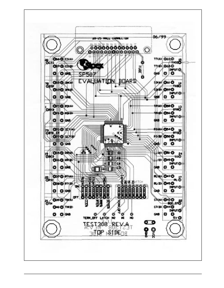
Evaluation Board (Rev. A) schematic is shown on
Figure 36. The SP507EB (Rev A.) layout plot is
shown on Figure 38.
SP505, 506 and SP507 Retrofits
Along with our SP506 Evaluation (SP506EB) and
SP507 Evaluation Boards (SP507EB), Sipex also
offers SP506 or SP507 Retrofit Boards (SP506RB
and SP507RB). Shown in Figure 37, these retrofit
boards are design to map onto existing motherboards
and replace an existing serial port platform. These
boards are approximately 1.375" x 1.375" and
contain the four charge pump capacitors and one
Schottky diode needed for compliant operation.
The boards also have the connections for driver
inputs and outputs and receiver inputs and outputs.
Using a ribbon type cable or "flex-board", the analog
I/Os can be mapped to the appropriate pin assignment
on the serial port connector and the TLL/CMOS
I/Os to the HDLC serial controller IC. The equipment's
existing serial transceiver ICs can be depopulated
and replaced by the retrofit board.
Sipex usually prefers to perform the retrofitting
in-house. But the experienced designer can also retrofit
the serial port as well. Once connected properly, the
functionality and electrical performance will be
transparent to the user. Sipex will perform the
necessary testing to ensure the retrofit is electrically
transparent and complaint to the physical layer
specifications. Sipex has already passed homologation
testing per NET1/2 and TBR2 with this board
retrofitted onto a router.
23
SP505/6/7APN/03
SP505, SP506, SP507 Application Note
© Copyright 2000 Sipex Corporation
Figure 38. SP507 Evaluation Board Layout

24
SP505/6/7APN/03
SP505, SP506, SP507 Application Note
© Copyright 2000 Sipex Corporation
More Compliancy....
In order for networking equipment to be
connected in the European network or even
offered in Europe, it must be thoroughly tested
to a set of specifications. Serial ports are no
exception to the rule and are tested to ensure
compliancy to their respective ITU specifications.
This is to ensure proper operation to the public
network as the equipment is connected. This is
a requirement in order to obtain the "CE" mark
for European compliance.
In January of 1998, CTR1/CTR2 compliancy
could officially be attained by using another test
option called TBR2. The Technical Basis for
Regulation specification was recently finalized
and approved for use as a test criteria for
certification. Similar to NET1/2, the testing
ensures that the serial port adheres to the ITU-T
V-Recommendations. It specifies the connector
type and the signals required between the DTE
and DCE. However, there are some minor
testing differences.
Paragraph 6.3.1 ≠ V.10 Interface
6.3.1.1 Generator open circuit output voltage
The single-ended generator or driver's output
(point A), for either binary state, shall be less
than or equal to 12.0V when terminated with a
3.9k
resistor to ground (point C).
6.3.1.3 Generator output rise/fall time
The driver output's transition from one binary
point to another shall be less than or equal to 0.3
of the nominal bit duration (t
b
). This is measured
between 10% and 90% of its steady state value
and with a 450
resistor load to ground.
6.3.1.4 Generator polarities
The driver's single-ended output A shall be:
a) greater than point C (V
OUT
> 0V) when the
signal condition 0 is transmitted for data
circuits, or ON for control circuits; and
b) less than point C (V
OUT
< 0V) when the signal
condition 1 is transmitted for data circuits, or
OFF for control circuits.
Figure 39. V.10 Driver Open Circuit Voltage
6.3.1.2 Generator terminated output voltage
The driver output's magnitude, for either binary
state, shall be greater than or equal to 2.0V when
terminated with a 450
resistor to ground.
Figure 40. V.10 Driver Terminated Voltage
Figure 41. V.10 Driver Transition Time
A
V
OC
3.9k
C
A
V
t
450
C
A
450
C
Oscilloscope

25
SP505/6/7APN/03
SP505, SP506, SP507 Application Note
© Copyright 2000 Sipex Corporation
Paragraph 6.3.2 ≠ V.11 Circuits
6.3.2.1 Generator open circuit output voltage
The magnitude of the driver's outputs for:
a) between point A and point B
b) either point A or point B to point C
shall be less than or equal to 12.0V for either
binary state when terminated with a 3.9k
resistor between points A and points B.
6.3.2.3 Generator output rise/fall time
The driver outputs' transition from one binary
point to another shall be less than or equal to 0.3
of the nominal bit duration (t
b
). This is measured
between 10% and 90% of its steady state value
and with a "Y" resistor configuration. The resistor
network contains two 50
resistors in series
with a center-tap 50
resistor between the two
series resistors to ground.
6.3.2.4 Generator polarities
The driver's point A output shall be:
a) greater than point B (V
A
≠V
B
> 0V) when the
signal condition 0 is transmitted for data circuits,
or ON for control circuits; and
b) less than point B (V
A
≠V
B
< 0V) when the
signal condition 1 is transmitted for data circuits,
or OFF for control circuits.
Figure 42. V.11 Driver Open Circuit Voltage
6.3.2.2 Generator terminated output voltage
The magnitude of the driver's outputs for:
a) between point A and point B
b) either point A or point B to point C
shall be greater than or equal to 2.0V for either
binary state when terminated with two 50
resistors connected in series between point A
and point B.
The center point of the two 50
resistors shall
measure less than or equal to 3.0V with respect
to point C.
Figure 43. V.11 Driver Output Terminated Voltage
Figure 44. V.11 Transition Time
Paragraph 6.3.3 ≠ V.28 Circuits
6.3.3.1 Generator open circuit output voltage
The single-ended generator or driver's output
(point A), for either binary state, shall be less
than or equal to 25.0V with respect to ground
(point C).
6.3.1.2 Generator terminated output voltage
The driver output's magnitude, for either binary
state, shall be greater than or equal to 3.0V when
terminated with a 3k
resistor to ground.
6.3.1.3 Generator output rise/fall time
The driver output's transition from one binary
point to another shall be less than or equal to 3%
or 1.0ms, whichever is greater, of the nominal
bit duration (t
b
). This is measured between +3V
and -3V of the transition and with 3k
resistor
// 2500pF loads to ground.
A
B
V
OC
3.9k
V
OCA
V
OCB
C
A
B
V
T
50
V
OS
C
50
A
B
50
C
50
50
Oscilloscope

26
SP505/6/7APN/03
SP505, SP506, SP507 Application Note
© Copyright 2000 Sipex Corporation
6.3.1.4 Generator polarities
The driver's single-ended output A shall be:
a) greater than point C (V
OUT
> 0V) when the
signal condition 0 is transmitted for data
circuits, or ON for control circuits; and
b) less than point C (V
OUT
< 0V) when the signal
condition 1 is transmitted for data circuits, or
OFF for control circuits.
6.3.3.5 Receiver maximum shunt capacitance
The total effective shunt capacitance shall be
less than 2500pF at point A with respect to
ground. This is measured by applying a 14V
P
signal with 0V offset at 9.6kbps with 50% duty
cycle through a 1.2k
resistor. The rise time
measured from -3V to +3V at point A to point C
(t
1
) and the fall time measured from +3V to -3V
at point A to point C (t
2
) is measured and recorded.
Then replace the receiver with a 3k
resistor in
parallel with a 2500pF capacitor and apply
the same signal through the 1.2k
resistor.
The new rise time (t
3
) is recorded and compared
to t
1
and t
2
. The times t
1
and t
2
shall be less than
or equal to t
3
.
Figure 45. V.28 Driver Open Circuit Voltage
Figure 46. V.28 Driver Terminated Voltage
Figure 47. V.28 Transition Time
Figure 48. V.28 Receiver Effective Shunt Capacitance
A
V
OC
C
A
V
T
C
3k
A
C
3k
2500pF
Oscilloscope
A
C
1.2k
9600bps, 14.0V
p-p
Square Wave
V
L

27
SP505/6/7APN/03
SP505, SP506, SP507 Application Note
© Copyright 2000 Sipex Corporation
Paragraph 6.3.4 ≠ V.35 Circuits
6.3.4.1 Generator open circuit output voltage
The magnitude of the driver's outputs for:
a) between point A and point B
b) either point A or point B to point C
shall be less than or equal to 1.2V for either
binary state when terminated with a 3.9k
resistor between points A and points B.
Figure 49. V.35 Driver Open Circuit Voltage
6.3.4.2 Generator terminated output voltage
The magnitude of the driver's outputs for:
a) between point A and point B
b) either point A or point B to point C
shall be 0.55V +20% for either binary state
when terminated with two 50
resistors
connected in series between point A and point B.
The center point of the two 50
resistors
shall measure less than or equal to 0.6V with
respect to point C.
Figure 50. V.35 Driver Terminated Voltage
6.3.4.3 Generator output rise/fall time
The driver outputs' transition from one binary
point to another shall be less than or equal to 0.1
of the nominal bit duration (t
b
). This is measured
between 20% and 80% of its steady state value
and with a "Y" resistor configuration. The
resistor network contains two 50
resistors in
series with a center-tap 50
resistor between
the two series resistors to ground.
6.3.4.4 Generator polarities
The driver's point A output shall be:
a) greater than point B (V
A
≠V
B
0V) when the
signal condition 0 is transmitted for data circuits,
or ON for control circuits; and
b) less than point B (V
A
≠V
B
0V) when the
signal condition 1 is transmitted for data circuits,
or OFF for control circuits.
Figure 51. V.35 Transition Time
The SP505 has been successfully tested to CTR1/
CTR2 through TUV Telecom Services. The test
was performed on the SP505EB Evaluation
Board. The test report CTR2/052101/98 can
be furnished upon request. The SP507 has
also successfully passed the CTR1/CTR2
testing requirements through KTL using our
SP507EB. The test report 9D2566DEU1 can
also be furnished upon request.
Please contact Sipex Applications for details.
A
B
V
OC
3.9k
V
OCA
V
OCB
C
A
B
50
C
50
V
T
V
OS
A
B
C
50
Oscilloscope
50
50

28
SP505/6/7APN/03
SP505, SP506, SP507 Application Note
© Copyright 2000 Sipex Corporation
Figure 52. Front Cover of the CTR1/CTR2 Test Report for the SP505

29
SP505/6/7APN/03
SP505, SP506, SP507 Application Note
© Copyright 2000 Sipex Corporation
Figure 53. Front Cover of the CTR1/CTR2 Test Report for the SP507

30
SP505/6/7APN/03
SP505, SP506, SP507 Application Note
© Copyright 2000 Sipex Corporation
ORDERING INFORMATION
Multi-Protocol Transceiver Products
Model
Temperature Range
Package Types
SP505CF ........................................................................... 0
∞
C to +70
∞
C ......................................................... 80≠pin JEDEC (BE-2 Outline) QFP
SP506CF ........................................................................... 0
∞
C to +70
∞
C ......................................................... 80≠pin JEDEC (BE-2 Outline) QFP
SP507CF ........................................................................... 0
∞
C to +70
∞
C ......................................................... 80≠pin JEDEC (BE-2 Outline) QFP
Evaluation and Retrofit Boards
Model
Description
SP505EB ........................................................................................................................................................................ SP505CF Evaluation Board
SP506EB ........................................................................................................................................................................ SP506CF Evaluation Board
SP507EB ........................................................................................................................................................................ SP507CF Evaluation Board
SP505RB ............................................................................................................................................................................. SP505CF Retrofit Board
SP506RB ............................................................................................................................................................................. SP506CF Retrofit Board
SP507RB ............................................................................................................................................................................. SP507CF Retrofit Board
Evaluation Kits
(Boxed with SP5xxEB, Product Datasheet, Application Note)
Model
Description
SP505EK .............................................................................................................................................................................. SP505CF Evaluation Kit
SP506EK .............................................................................................................................................................................. SP506CF Evaluation Kit
SP507EK .............................................................................................................................................................................. SP507CF Evaluation Kit
Corporation
SIGNAL PROCESSING EXCELLENCE
Sipex Corporation reserves the right to make changes to any products described herein. Sipex does not assume any liability arising out of the
application or use of any product or circuit described hereing; neither does it convey any license under its patent rights nor the rights of others.
Sipex Corporation
Headquarters and
Sales Office
22 Linnell Circle
Billerica, MA 01821
TEL: (978) 667-8700
FAX: (978) 670-9001
e-mail: sales@sipex.com
Sales Office
233 South Hillview Drive
Milpitas, CA 95035
TEL: (408) 934-7500
FAX: (408) 935-7600